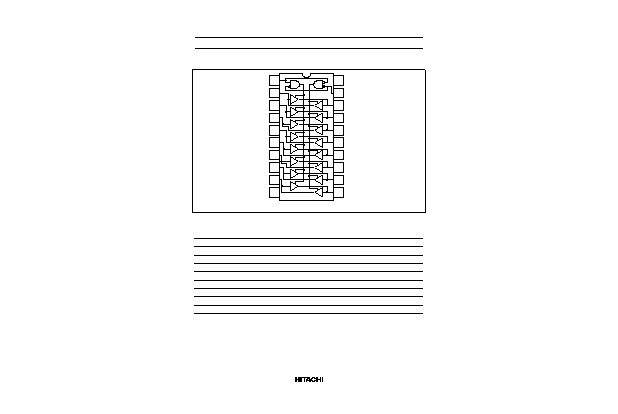
ChipFind - документация

Электронный компонент: HD74HC245

Скачать:  PDF   ZIP
HD74HC245
Octal Bus Transceivers (with 3-state outputs)
Description
Each device has an active low enable input
G and a direction control input, DIR. When DIR is high, data
flows from the A inputs to the B outputs. When DIR is low, data flows from the B inputs to the A outputs.
The HD74HC245 transfers true data from one bus to the other. This device does not have schmitt trigger
inputs.
Features
High Speed Operation: t
pd
= 8 ns typ (C
L
= 50 pF)
High Output Current: Fanout of 15 LSTTL Loads
Wide Operating Voltage: V
CC
= 2 to 6 V
Low Input Current: 1 A max
Low Quiescent Supply Current: I
CC
(static) = 4 A max (Ta = 25C)
Function Table
Enable G
Direction Control DIR
Operation
L
L
B data to A bus
L
H
A data to B bus
H
X
Isolation
H :
high level
L
:
low level
X :
irrelevant
HD74HC245
2
Pin Arrangement
1
2
3
4
5
6
7
8
9
10
DIR
A
1
A
2
A
3
A
4
A
5
A
6
A
7
A
8
GND
V
CC
B
1
B
2
B
3
B
4
B
5
B
6
B
7
B
8
Enable
G
20
19
18
17
16
15
14
13
12
11
(Top view)
Absolute Maximum Ratings
Item
Symbol
Rating
Unit
Supply voltage range
V
CC
0.5 to +7.0
V
Input voltage
V
IN
0.5 to V
CC
+ 0.5
V
Output voltage
V
OUT
0.5 to V
CC
+ 0.5
V
DC current drain per pin
I
OUT
35
mA
DC current drain per V
CC
, GND
I
CC
, I
GND
75
mA
DC input diode current
I
IK
20
mA
DC output diode current
I
OK
20
mA
Power dissipation per package
P
T
500
mW
Storage temperature
Tstg
65 to +150
C
HD74HC245
3
DC Characteristics
Ta = 25
C
Ta = 40 to
+85
C
Item
Symbol
V
CC
(V) Min Typ Max Min
Max
Unit
Test Conditions
Input voltage
V
IH
2.0
1.5
--
--
1.5
--
V
4.5
3.15 --
--
3.15
--
6.0
4.2
--
--
4.2
--
V
IL
2.0
--
--
0.5
--
0.5
V
4.5
--
--
1.35 --
1.35
6.0
--
--
1.8
--
1.8
Output voltage
V
OH
2.0
1.9
2.0
--
1.9
--
V
Vin = V
IH
or V
IL
I
OH
= 20
A
4.5
4.4
4.5
--
4.4
--
6.0
5.9
6.0
--
5.9
--
4.5
4.18 --
--
4.13
--
I
OH
= 6 mA
6.0
5.68 --
--
5.63
--
I
OH
= 7.8 mA
V
OL
2.0
--
0.0
0.1
--
0.1
V
Vin = V
IH
or V
IL
I
OL
= 20
A
4.5
--
0.0
0.1
--
0.1
6.0
--
0.0
0.1
--
0.1
4.5
--
--
0.26 --
0.33
I
OL
= 6 mA
6.0
--
--
0.26 --
0.33
I
OL
= 7.8 mA
Off-state output
current
I
OZ
6.0
--
--
0.5 --
5.0
A
Vin = V
IH
or V
IL
,
Vout = V
CC
or GND
Input current
Iin
6.0
--
--
0.1 --
1.0
A
Vin = V
CC
or GND
Quiescent supply
current
I
CC
6.0
--
--
4.0
--
40
A
Vin = V
CC
or GND, Iout = 0
A
HD74HC245
4
AC Characteristics (C
L
= 50 pF, Input t
r
= t
f
= 6 ns)
Ta = 25
C
Ta = 40 to
+85
C
Item
Symbol
V
CC
(V) Min Typ Max Min
Max
Unit
Test Conditions
Propagation delay t
PLH
2.0
--
--
90
--
115
ns
time
4.5
--
8
18
--
23
6.0
--
--
15
--
20
t
PHL
2.0
--
--
90
--
115
ns
4.5
--
8
18
--
23
6.0
--
--
15
--
20
Output enable
t
ZL
2.0
--
--
150 --
190
ns
time
4.5
--
16
30
--
38
6.0
--
--
26
--
32
t
ZH
2.0
--
--
150 --
190
ns
4.5
--
12
30
--
38
6.0
--
--
26
--
32
Output disable
t
LZ
2.0
--
--
150 --
190
ns
time
4.5
--
17
30
--
38
6.0
--
--
26
--
32
t
HZ
2.0
--
--
150 --
190
ns
4.5
--
18
30
--
38
6.0
--
--
26
--
32
Output rise/fall
t
TLH
2.0
--
--
60
--
75
ns
time
t
THL
4.5
--
4
12
--
15
6.0
--
--
10
--
13
Input capacitance
Cin
--
--
5
10
--
10
pF
Hitachi Code
JEDEC
EIAJ
Weight (reference value)
DP-20N
--
Conforms
1.26 g
Unit: mm
0.51 Min
2.54 Min
5.08 Max
7.62
0.25
+ 0.11
0.05
2.54
0.25
0.48
0.10
24.50
25.40 Max
0.89
1.30
6.30
7.00 Max
1
10
11
20
0
15
1.27 Max