ChipFind - документация

Электронный компонент: HD74HC258

Скачать:  PDF   ZIP
HD74HC258
Quad. 2-to-1-line Data Selectors/Multiplexers
(with 3-state outputs)
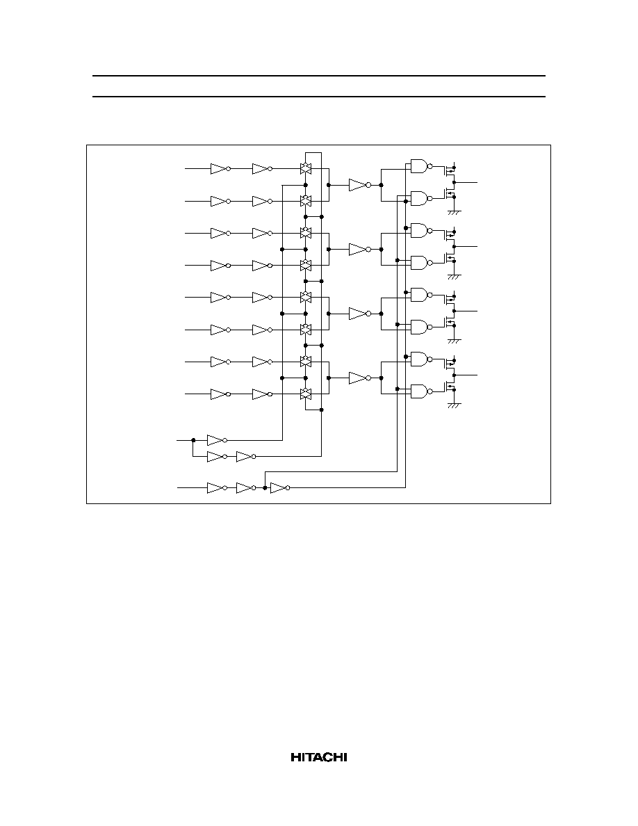
Description
The large output drive capability coupled with the 3-state feature make this device ideal for interfacing with
bus lines in a bus organized system. When the output control input line is taken high, the outputs of all four
multiplexers are sent into a high impedance state. When the output control line is low, the select input
chooses whether the A or B input is used.
Features
High Speed Operation: t
pd
(Data to Y) = 11 ns typ (C
L
= 50 pF)
High Output Current: Fanout of 15 LSTTL Loads
Wide Operating Voltage: V
CC
= 2 to 6 V
Low Input Current: 1 A max
Low Quiescent Supply Current: I
CC
(static) = 4 A max (Ta = 25C)
Function Table
Inputs
Outputs
Output Control
Select
A
B
Y
H
X
X
X
Z
L
L
L
X
H
L
L
H
X
L
L
H
X
L
H
L
H
X
H
L
Notes H: high level
L : low level
X: irrelevant
Z: off (high-impedance) state of a 3-state output
HD74HC258
2
Pin Arrangement
(Top view)
1
2
3
4
5
6
7
8
Select
1A
1B
1Y
2A
2B
2Y
GND
Outputs
Outputs
Inputs
Inputs
V
CC
4A
4B
4Y
3A
3B
3Y
16
15
14
13
12
11
10
9
1A
1B
1Y
2A
2B
2Y
G
4A
4B
4Y
3A
3B
S
3Y
Output
Output
Inputs
Inputs
Output
cotrol
Absolute Maximum Ratings
Item
Symbol
Rating
Unit
Supply voltage range
V
CC
0.5 to +7.0
V
Input voltage
V
IN
0.5 to V
CC
+ 0.5
V
Output voltage
V
OUT
0.5 to V
CC
+ 0.5
V
DC current drain per pin
I
OUT
35
mA
DC current drain per V
CC
, GND
I
CC
, I
GND
75
mA
DC input diode current
I
IK
20
mA
DC output diode current
I
OK
20
mA
Power dissipation per package
P
T
500
mW
Storage temperature
Tstg
65 to +150
C
HD74HC258
3
Logic Diagram
Select
Output
control
1A
1B
2A
2B
3A
3B
4A
4B
1Y
2Y
3Y
4Y
V
CC
V
CC
V
CC
V
CC
HD74HC258
4
DC Characteristics
Ta = 25
C
Ta = 40 to
+85
C
Item
Symbol
V
CC
(V) Min Typ Max Min
Max
Unit
Test Conditions
Input voltage
V
IH
2.0
1.5
--
--
1.5
--
V
4.5
3.15 --
--
3.15
--
6.0
4.2
--
--
4.2
--
V
IL
2.0
--
--
0.5
--
0.5
V
4.5
--
--
1.35 --
1.35
6.0
--
--
1.8
--
1.8
Output voltage
V
OH
2.0
1.9
2.0
--
1.9
--
V
Vin = V
IH
or V
IL
I
OH
= 20
A
4.5
4.4
4.5
--
4.4
--
6.0
5.9
6.0
--
5.9
--
4.5
4.18 --
--
4.13
--
I
OH
= 6 mA
6.0
5.68 --
--
5.63
--
I
OH
= 7.8 mA
V
OL
2.0
--
0.0
0.1
--
0.1
V
Vin = V
IH
or V
IL
I
OL
= 20
A
4.5
--
0.0
0.1
--
0.1
6.0
--
0.0
0.1
--
0.1
4.5
--
--
0.26 --
0.33
I
OL
= 6 mA
6.0
--
--
0.26 --
0.33
I
OL
= 7.8 mA
Off-state output
current
I
OZ
6.0
--
--
0.5 --
5.0
A
Vin = V
IH
or V
IL
,
Vout = V
CC
or GND
Input current
Iin
6.0
--
--
0.1 --
1.0
A
Vin = V
CC
or GND
Quiescent supply
current
I
CC
6.0
--
--
4.0
--
40
A
Vin = V
CC
or GND, Iout = 0
A
HD74HC258
5
AC Characteristics (C
L
= 50 pF, Input t
r
= t
f
= 6 ns)
Ta = 25
C
Ta = 40 to
+85
C
Item
Symbol
V
CC
(V) Min Typ Max Min
Max
Unit
Test Conditions
Propagation delay t
PLH
2.0
--
--
115 --
145
ns
Data to Y
time
t
PHL
4.5
--
11
23
--
29
6.0
--
--
20
--
25
2.0
--
--
115 --
145
Select to Y
4.5
--
13
23
--
29
6.0
--
--
20
--
25
Output enable
t
ZL
2.0
--
--
150 --
190
ns
time
4.5
--
11
30
--
38
6.0
--
--
26
--
33
t
ZH
2.0
--
--
150 --
190
ns
4.5
--
13
30
--
38
6.0
--
--
26
--
33
Output disable
t
LZ
2.0
--
--
150 --
190
ns
time
4.5
--
13
30
--
38
6.0
--
--
26
--
33
t
HZ
2.0
--
--
150 --
190
ns
4.5
--
18
30
--
38
6.0
--
--
26
--
33
Output rise/fall
t
TLH
2.0
--
--
60
--
75
ns
time
t
THL
4.5
--
4
12
--
15
6.0
--
--
10
--
13
Input capacitance
Cin
--
--
5
10
--
10
pF