Äîêóìåíòàöèÿ è îïèñàíèÿ www.docs.chipfind.ru
HM658512A Series
4 M PSRAM (512-kword
×
8-bit)
2 k Refresh
ADE-203-218C(Z)
Rev. 3.0
Nov. 1997
Description
The Hitachi HM658512A is a CMOS pseudo static RAM organized 512-kword
×
8-bit. It realizes higher
density, higher performance and low power consumption by employing 0.8 µm Hi-CMOS process
technology.
It offers low power data retention by self refresh mode. It also offers easy non multiplexed address
interface and easy refresh functions. HM658512A is suitable for handy systems which work with battery
back-up systems.
The device is packaged in a small 525-mil SOP (460-mil body SOP) or a 8
×
20 mm TSOP with thickness
of 1.2 mm, or a 600-mil plastic DIP. High density custom cards made of Tape Carrier Packages are also
available.
Features
·
Single 5 V (±10%)
·
High speed
Access time
CE access time: 70/80/100 ns (max)
Cycle time
Random read/write cycle time:
115/130/160 ns (min)
·
Low power
Active: 250 mW (typ)
Standby: 200 µW (typ)
·
Directly TTL compatible
All inputs and outputs
·
Simple address configuration
Non multiplexed address
·
Refresh cycle
2048 refresh cycles: 32 ms
HM658512A Series
2
·
Easy refresh functions
Address refresh
Automatic refresh
Self refresh
Ordering Information
Type No.
Access time
Package
HM658512ALP-7
HM658512ALP-8
HM658512ALP-10
70 ns
80 ns
100 ns
600-mil 32-pin plastic DIP (DP-32)
HM658512ALP-7V
HM658512ALP-8V
HM658512ALP-10V
70 ns
80 ns
100 ns
HM658512ALFP-7
HM658512ALFP-8
HM658512ALFP-10
70 ns
80 ns
100 ns
525-mil 32-pin plastic SOP (FP-32D)
HM658512ALFP-7V
HM658512ALFP-8V
HM658512ALFP-10V
70 ns
80 ns
100 ns
HM658512ALTT-7
HM658512ALTT-8
HM658512ALTT-10
70 ns
80 ns
100 ns
400-mil 32-pin plastic TSOP (TTP-32D)
HM658512ALTT-7V
HM658512ALTT-8V
HM658512ALTT-10V
70 ns
80 ns
100 ns
HM658512ALRR-7
HM658512ALRR-8
HM658512ALRR-10
70 ns
80 ns
100 ns
400-mil 32-pin plastic TSOP (TTP-32DR)
HM658512ALRR-7V
HM658512ALRR-8V
HM658512ALRR-10V
70 ns
80 ns
100 ns
HM658512A Series
3
Pin Arrangement
1
2
3
4
5
6
7
8
9
10
11
12
13
14
15
16
32
31
30
29
28
27
26
25
24
23
22
21
20
19
18
17
A18
A16
A14
A12
A7
A6
A5
A4
A3
A2
A1
A0
I/O0
I/O1
I/O2
V
SS
V
A15
A17
WE
A13
A8
A9
A11
OE/RFSH
A10
CE
I/O7
I/O6
I/O5
I/O4
I/O3
CC
HM658512ALP/ALFP Series
(Top view)
1
2
3
4
5
6
7
8
9
10
11
12
13
14
15
16
32
31
30
29
28
27
26
25
24
23
22
21
20
19
18
17
SS
V
A15
A17
WE
A13
A8
A9
A11
OE/RFSH
A10
CE
I/O7
I/O6
I/O5
I/O4
I/O3
A18
A16
A14
A12
A7
A6
A5
A4
A3
A2
A1
A0
I/O0
I/O1
I/O2
V
CC
HM658512ALTT Series
(Top view)
HM658512A Series
4
Pin Arrangement (cont.)
1
2
3
4
5
6
7
8
9
10
11
12
13
14
15
16
32
31
30
29
28
27
26
25
24
23
22
21
20
19
18
17
SS
V
A15
A17
WE
A13
A8
A9
A11
OE/RFSH
A10
CE
I/O7
I/O6
I/O5
I/O4
I/O3
A18
A16
A14
A12
A7
A6
A5
A4
A3
A2
A1
A0
I/O0
I/O1
I/O2
V
CC
HM658512ALRR Series
(Top view)
Pin Description
Pin name
Function
A0 to A18
Address
I/O0 to I/O7
Input/Output
CE
Chip enable
OE
/
RFSH
Output enable/Refresh
WE
Write enable
V
CC
Power supply
V
SS
Ground
HM658512A Series
5
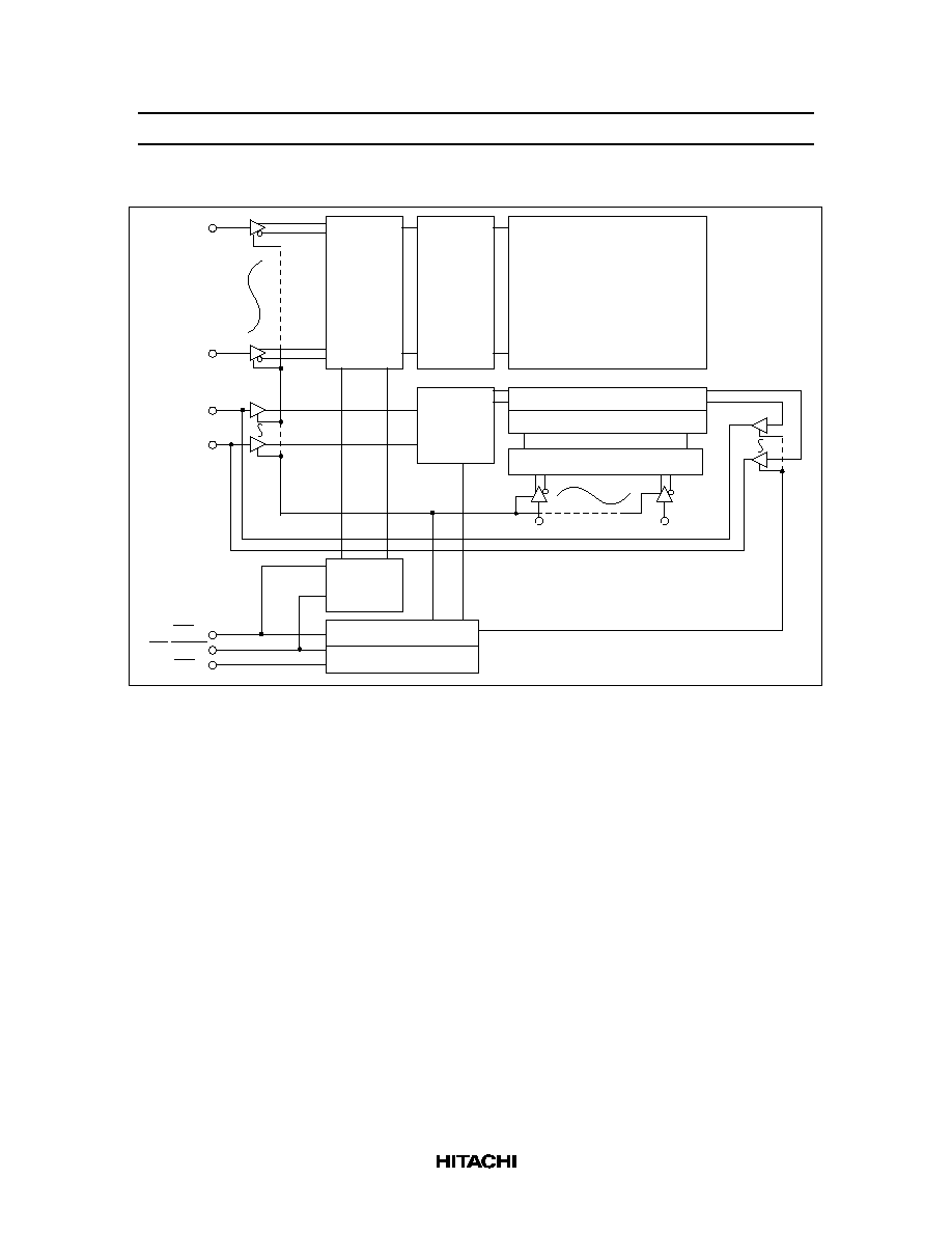
Block Diagram
Refresh
Control
Timing Pulse Gen.
Read Write Control
Address Latch Control
Column Decoder
Column I/O
Memory Matrix
Row
Decoder
Address
Latch
Control
Input
Data
Control
CE
WE
I/O 7
I/O 0
A0
A10
A11
A18
OE/RFSH
(2048
×
256)
×
8

HM658512A Series
6
Pin Functions
CE: Chip Enable (Input)
CE is a basic clock. RAM is active when CE is low, and is on standby when CE is high.
A0 to A18: Address Inputs (Input)
A0 to A10 are row addresses and A11 to A18 are column addresses. The entire addresses A0 to A18
are fetched into RAM by the falling edge of
CE.
OE/RFSH: Output Enable/Refresh (Input)
This pin has two functions. Basically it works as
OE when CE is low, and as RFSH when CE is high
(in standby mode). After a read or write cycle finishes, refresh does not start if
CE goes high while
OE/RFSH is held low. In order to start a refresh in standby mode, OE/RFSH must go high to reset the
refresh circuits of the RAM. After the refresh circuits are reset, the refresh starts when
OE/RFSH goes
low.
I/O0 to I/O7: Input/Output (Inputs and Outputs) These pins are data I/O pins.
WE: Write Enable (Input)
RAM is in write mode when
WE is low, and is in read mode when WE is high. I/O data is fetched into
RAM by the rising edge of
WE or CE (earlier timing) and the data is written into memory cells.
Refresh
There are three refresh modes : address refresh, automatic refresh and self refresh.
(1) Address refresh: Data is refreshed by accessing all 2048 row addresses every 32 ms. A read is one
method of accessing those addresses. Each row address (2048 addresses of A0 to A10)must be read at
least once every 32 ms. In address refresh mode,
OE/RFSH can remain high. In this case, the I/O pins
remain at high impedance, but the refresh is done within RAM.
(2) Automatic refresh: Instead of address refresh, automatic refresh can be used. RAM goes to automatic
refresh mode if
OE/RFSH falls while CE is high and it remains low for at least t
FAP
. One automatic
refresh cycle is executed by one low pulse of
OE/RFSH. It is not necessary to input the refresh
address from outside since it is generated internally by an on-chip address counter. 2048 automatic
refresh cycles must be done every 32 ms.
(3) Self refresh: Self refresh mode is suitable for data retention by battery. In standby mode, a self refresh
starts automatically when
OE/RFSH stays low for more than 8 µs. Refresh addresses are automatically
specified by the on-chip address counter, and the refresh period is determined by the on-chip timer.
Automatic refresh and self refresh are distinguished from each other by the width of the
OE/RFSH low
pulse in standby mode. If the
OE/RFSH low pulse is wider than 8 µs, RAM becomes into self refresh
mode; if the
OE/RFSH low pulse is less than 8 µs, it is recognized as an automatic refresh instruction.
HM658512A Series
7
At the end of self refresh, refresh reset time (t
RFS
) is required to reset the internal self refresh operation of
the RAM. During t
RFS
,
CE and OE/RFSH must be kept high. If auto refresh follows self refresh, low
transition of
OE/RFSH at the beginning of automatic refresh must not occur during t
RFS
period.
Notes on Using the HM658512A
Since pseudo static RAM consists of dynamic circuits like DRAM, its clock pins are more noise-sensitive
than conventional SRAM's.
(1) If a short
CE pulse of a width less than t
CE
min is applied to RAM, an incomplete read occurs and
stored data may be destroyed. Make sure that
CE low pulses of less than t
CE
min are inhibited. Note
that a 10 ns
CE low pulse may sometimes occur owing to the gate delay on the board if the CE signal is
generated by the decoding of higher address signals on the board. Avoid these short pulses.
(2)
OE/RFSH works as refresh control in standby mode. A short OE/RFSH low pulse may cause an
incomplete refresh that will destroy data. Make sure that
OE/RFSH low pulse of less than t
FAP
min are
also inhibited.
(3) t
OHC
and t
OCD
are the timing specs which distinguish the
OE function of OE/RFSH from the RFSH
function. The t
OHC
and t
OCD
specs must be strictly maintained.
(4) Start the HM658512A operating by executing at least eight initial cycles (dummy cycles) at least 100
µs after the power voltage reaches 4.5 V-5.5 V after power-on.
Function Table
CE
OE
/
RFSH
WE
I/O pin
Mode
L
L
H
Dout
Read
L
X
L
High-Z
Write
L
H
H
High-Z
--
H
L
X
High-Z
Refresh
H
H
X
High-Z
Standby
Note:
X means H or L.
HM658512A Series
8
Absolute Maximum Ratings
Parameter
Symbol
Value
Unit
Note
Terminal voltage with respect to V
SS
V
T
1.0 to +7.0
V
1
Power dissipation
P
T
1.0
W
Operating temperature
Topr
0 to +70
°
C
Storage temperature
Tstg
55 to +125
°
C
Storage temperature under bias
Tbias
10 to +85
°
C
Note:
1. With respect to V
SS
Recommended DC Operating Conditions (Ta = 0 to +70°C)
Parameter
Symbol
Min
Typ
Max
Unit
Notes
Supply voltage
V
CC
4.5
5.0
5.5
V
V
SS
0
0
0
V
Input voltage
V
IH
2.4
--
6.0
V
V
IL
1.0
--
0.8
V
1
Note:
1. V
IL
min = 3.0 V for pulse width 30 ns
HM658512A Series
9
DC Characteristics (Ta = 0 to +70°C, V
CC
= 5 V ± 10 %, V
SS
= 0 V)
Parameter
Symbol Min
Typ
Max Unit Test conditions
Notes
Operating power supply current I
CC1
--
--
75
mA
I
I/O
= 0 mA
t
cyc
= min
Standby power supply current
I
SB1
--
1
2
mA
CE
= V
IH
, Vin
0 V
OE
/
RFSH
= V
IH
I
SB2
--
20
200
µ
A
CE
V
CC
0.2 V, Vin
0 V,
OE
/
RFSH
V
CC
0.2 V
1
100
µ
A
CE
V
CC
0.2 V, Vin
0 V,
OE
/
RFSH
V
CC
0.2 V
2
Operating power supply current
in self refresh mode
I
CC2
--
1
2
mA
CE
= V
IH
, Vin
0 V,
OE
/
RFSH
= V
IL
I
CC3
--
70
200
µ
A
CE
V
CC
0.2 V, Vin
0 V,
OE
/
RFSH
0.2 V
1
40
100
µ
A
CE
V
CC
0.2 V, Vin
0 V,
OE
/
RFSH
0.2 V
2
Input leakage current
I
LI
10
--
10
µ
A
V
CC
= 5.5 V, Vin = V
SS
to V
CC
Output leakage current
I
LO
10
--
10
µ
A
OE
/
RFSH
= V
IH
V
I/O
= V
SS
to V
CC
Output voltage
V
OL
--
--
0.4
V
I
OL
= 2.1 mA
V
OH
2.4
--
--
V
I
OH
= 1 mA
Notes: 1. Only for L-version.
2. Only for V-version.
Capacitance (Ta = 25°C, f = 1 MHz)
Parameter
Symbol
Typ
Max
Unit
Test conditions
Input capacitance
C
in
--
8
pF
V
in
= 0 V
Input /output capacitance
C
I/O
--
10
pF
V
I/O
= 0 V
Note : This parameter is sampled and not 100% tested.
HM658512A Series
10
AC Characteristics (Ta = 0 to +70°C, V
CC
= 5 V ± 10%, unless otherwise noted.)
Test Conditions
·
Input pulse levels: 0.4 V, 2.4 V
·
Input rise and fall time: 5 ns
·
Timing measurement level: 0.8 V, 2.2 V
·
Reference levels: V
OH
= 2.0 V, V
OL
= 0.8 V
·
Output load: 1 TTL Gate and C
L
(100 pF) (Including scope and jig)
HM658512A
-7
-8
-10
Parameter
Symbol Min
Max
Min
Max
Min
Max
Unit
Notes
Random read or write cycle time
t
RC
115
--
130
--
160
--
ns
Chip enable access time
t
CEA
--
70
--
80
--
100
ns
Read-modify- write cycle time
t
RWC
160
--
180
--
220
--
ns
Output enable access time
t
OEA
--
25
--
30
--
40
ns
Chip disable to output in high-Z
t
CHZ
0
25
0
25
0
25
ns
1, 2
Chip enable to output in low-Z
t
CLZ
20
--
20
--
20
--
ns
2
Output disable to output in high-Z
t
OHZ
--
25
--
25
--
25
ns
1, 2
Output enable to output in low-Z
t
OLZ
0
--
0
--
0
--
ns
2
Chip enable pulse width
t
CE
70 n
10
µ
80 n
10
µ
100 n 10
µ
s
Chip enable precharge time
t
P
35
--
40
--
50
--
ns
Address setup time
t
AS
0
--
0
--
0
--
ns
Address hold time
t
AH
20
--
20
--
25
--
ns
Read command setup time
t
RCS
0
--
0
--
0
--
ns
Read command hold time
t
RCH
0
--
0
--
0
--
ns
Write command pulse width
t
WP
25
--
25
--
30
--
ns
Chip enable to end of write
t
CW
70
--
80
--
100
--
ns
Chip enable to output enable delay
time
t
OCD
0
--
0
--
0
--
ns
Output enable hold time
t
OHC
0
--
0
--
0
--
ns
HM658512A Series
11
AC Characteristics (Ta = 0 to +70°C, V
CC
= 5 V ± 10%, unless otherwise noted.) (cont.)
HM658512A
-7
-8
-10
Parameter
Symbol Min
Max
Min
Max
Min
Max
Unit
Notes
Data in to end of write
t
DW
20
--
20
--
25
--
ns
Data in hold time for write
t
DH
0
--
0
--
0
--
ns
Output active from end of write
t
OW
5
--
5
--
5
--
ns
2
Write to output in high-Z
t
WHZ
--
20
--
20
--
25
ns
1, 2
Transition time (rise and fall)
t
T
3
50
3
50
3
50
ns
6
Refresh command delay time
t
RFD
35
--
40
--
50
--
ns
Refresh precharge time
t
FP
35
--
40
--
40
--
ns
Refresh command pulse width for
automatic refresh
t
FAP
70 n
8
µ
80 n
8
µ
80 n
8
µ
s
Automatic refresh cycle time
t
FC
115
--
130
--
160
--
ns
Refresh command pulse width for
self refresh
t
FAS
8
--
8
--
8
--
µ
s
Refresh reset time from self refresh t
RFS
600
--
600
--
600
--
ns
9
Refresh period
t
REF
--
32
--
32
--
32
ms
2048
cycle
Notes: 1. t
CHZ
, t
OHZ
, t
WHZ
are defined as the time at which the output achieves the open circuit condition.
2. t
CHZ
, t
CLZ
, t
OHZ
, t
OLZ
, t
WHZ
and t
OW
are sampled under the condition of t
T
= 5 ns and not 100% tested.
3. A write occurs during the overlap of low
CE
and low
WE
. Write end is defined at the earlier of
WE
going high or
CE
going high.
4. If the
CE
low transition occurs simultaneously with or from the
WE
low transition, the output
buffers remain in high impedance state.
5. In write cycle,
OE
or
WE
must disable output buffers prior to applying data to the device and at
the end of write cycle data inputs must be floated prior to
OE
or
WE
turning on output buffers.
During this period, I/O pins are in the output state, therefore the input signals of opposite phase
to the outputs must not be applied.
6. Transition time t
T
is measured between V
IH
(min) and V
IL
(max). V
IH
(min) and V
IL
(max) are
reference levels for measuring timing of input signals.
7. After power-up, pause for more than 100
µ
s and execute at least 8 initialization cycles.
8. 2048 cycles of burst refresh or the first cycle of distributed automatic refresh must be executed
within 15
µ
s after self refresh, in order to meet the refresh specification of 32 ms and 2048
cycles.
9. At the end of self refresh, refresh reset time (t
RFS
) is required to reset the internal self refresh
operation of the RAM. During t
RFS
,
CE
and
OE
/
RFSH
must be kept high. If automatic refresh
follows self refresh, low transition of
OE
/
RFSH
at the beginning of automatic refresh must not
occur during t
RFS
period.
HM658512A Series
12
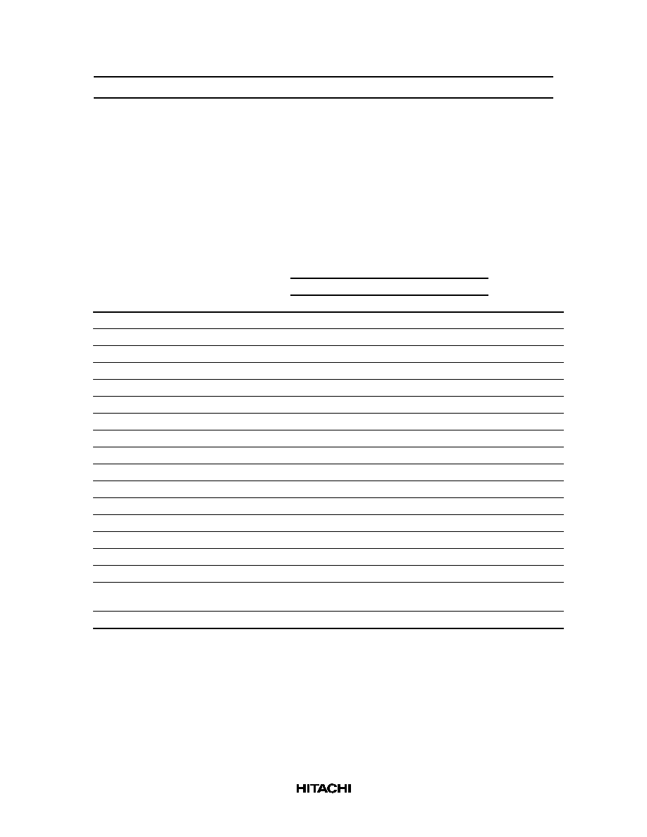
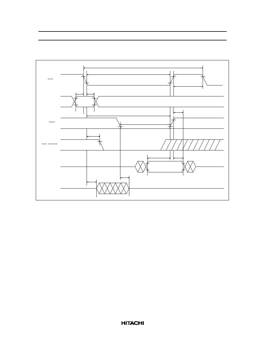
Timing Waveform
Read Cycle
t
CE
Address
A0 to A18
WE
OE/RFSH
t
t
t
t
Valid
t
t
t
t
Dout
t
Valid data out
t
t
t
RC
CE
AS
AH
P
RCH
CHZ
OHZ
OEA
CEA
OHC
RCS
OLZ
HM658512A Series
13
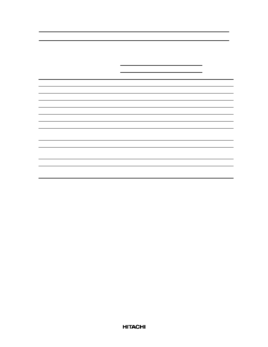
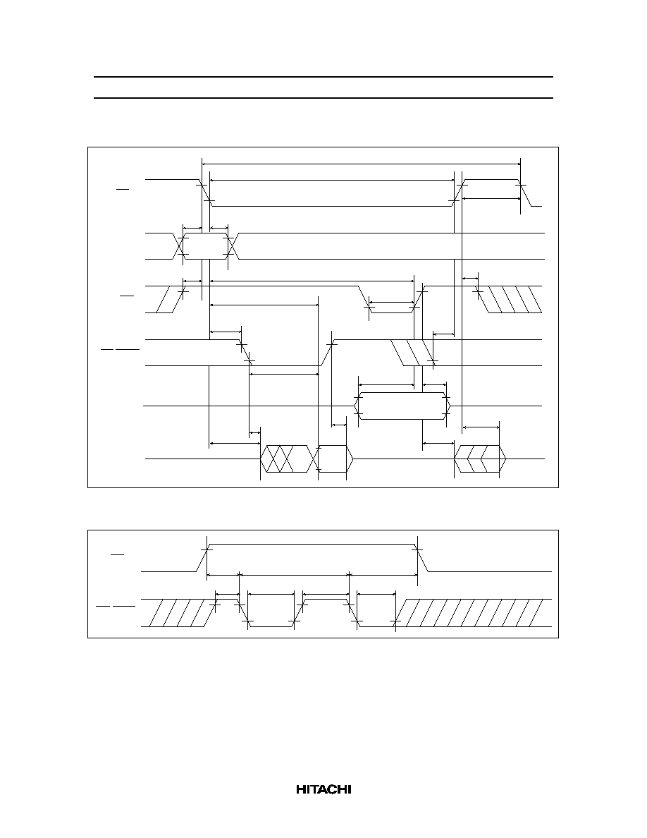
Write Cycle (1) (
OE high)
CE
Address
A0 to A18
WE
OE/RFSH
Din
t
t
t
t
t
Valid
Dout
Valid
Data in
t
t
t
t
t
t
t
t
t
t
RC
CE
AS
AH
CW
CLZ
OHZ
WHZ
WP
OCD
P
DW
DH
OLZ
OW
HM658512A Series
14
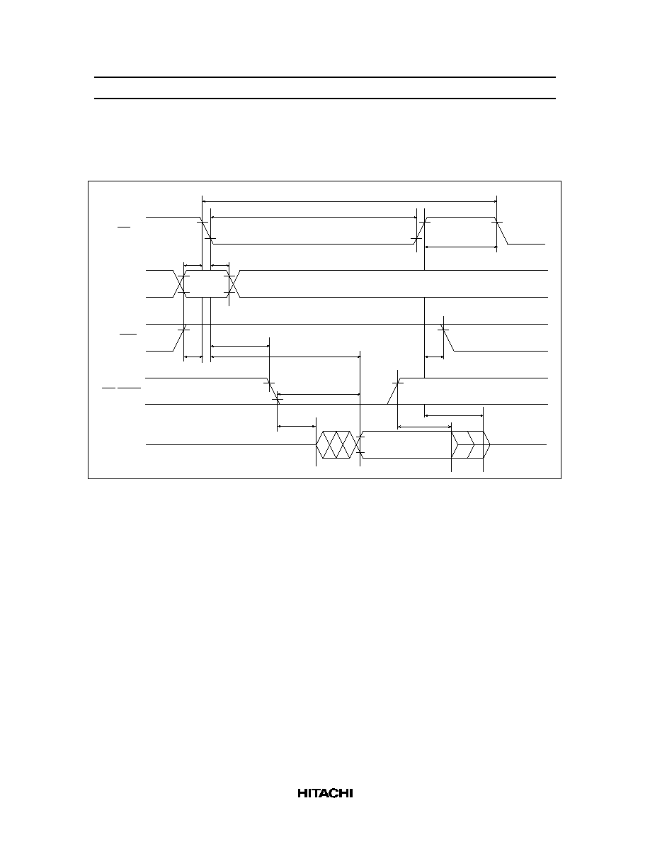
Write Cycle (2) (
OE low)
CE
Address
A0 to A18
WE
OE/RFSH
Din
t
t
t
t
t
Valid
Dout
Valid data in
t
t
t
t
t
t
t
t
RC
CE
P
DH
CW
WP
DH
DW
WHZ
CLZ
OHC
AH
AS
HM658512A Series
15
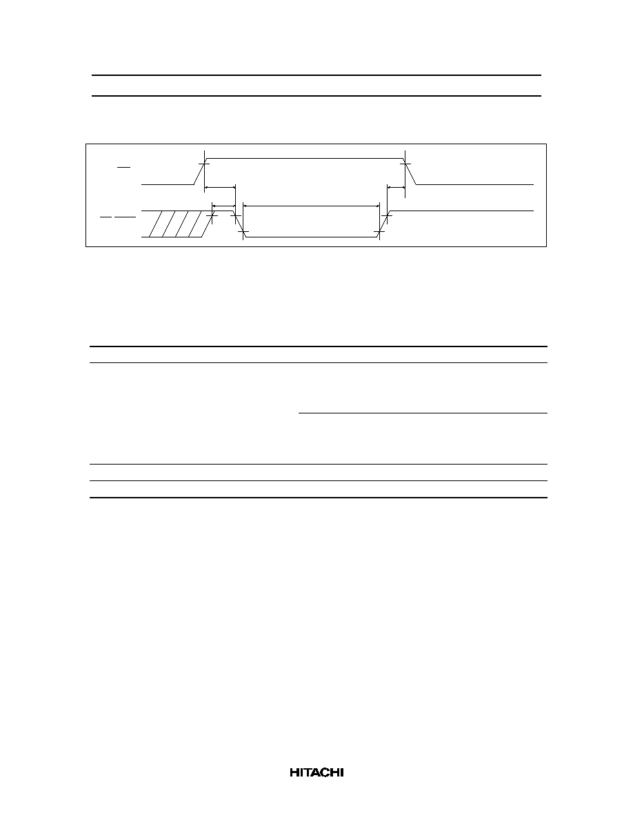
Read-Modify-Write Cycle
CE
Address
A0 to A18
WE
OE/RFSH
Din
t
t
t
t
t
Valid
Dout
Valid data in
t
t
t
t
t
t
t
t
t
Valid
data
out
t
t
t
t
t
t
RWC
CE
CW
P
RCH
OCD
WP
DH
DW
CHZ
OW
AS
AH
RCS
CEA
OHC
OEA
OLZ
CLZ
OHZ
Automatic Refresh Cycle
CE
OE/RFSH
t
t
t
t
t
t
t
RFD
FC
FP
FAP
FP
FAP
FC
HM658512A Series
16
Self Refresh Cycle
CE
OE/RFSH
t
t
t
t
RFD
FP
FAS
RFS
Low V
CC
Data Retention Characteristics (Ta = 0 to +70
°
C)
This characteristics is guaranteed only for V-version.
Parameter
Symbol
Min
Typ
Max
Unit
Test conditions
V
CC
for data retention
V
DR
3.0
--
5.5
V
Self refresh current
I
CCDR
--
--
50
µ
A
V
CC
= 3.0 V,
CE
V
CC
0.2 V
OE
/
RFSH
0.2
Vin
0 V
--
--
100
µ
A
V
CC
= 5.5 V,
CE
V
CC
0.2 V
OE
/
RFSH
0.2
Vin
0 V
Refresh setup time
t
FS
0
--
--
ns
Operation recovery time
t
FR
5
--
--
ms
HM658512A Series
17
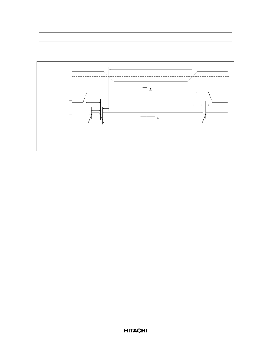
Low V
CC
Data Retention Timing Waveform
Data Retention mode
VDR
FAS
FS
FR
RFS
t
FP
4.5V
2.4V
0.8V
2.4V
0.8V
V
CE
OE/RFSH
CE
Vcc-0.2V
OE/RFSH
0.2V
CC
RFD
t
t
t
t
t
Notes:
1.
Rise time and fall time of power supply voltage must be smaller than 0.05 V/ms.
2.
Keep
CE
V
CC
0.2 V during data retention mode.
3.
Regarding t
RFD
, t
FP
, t
FAS
and t
RFS
, refer to AC characteristics.
4.
Input voltage should be lower than V
CC
+1.5 V in data retention mode.
HM658512A Series
18
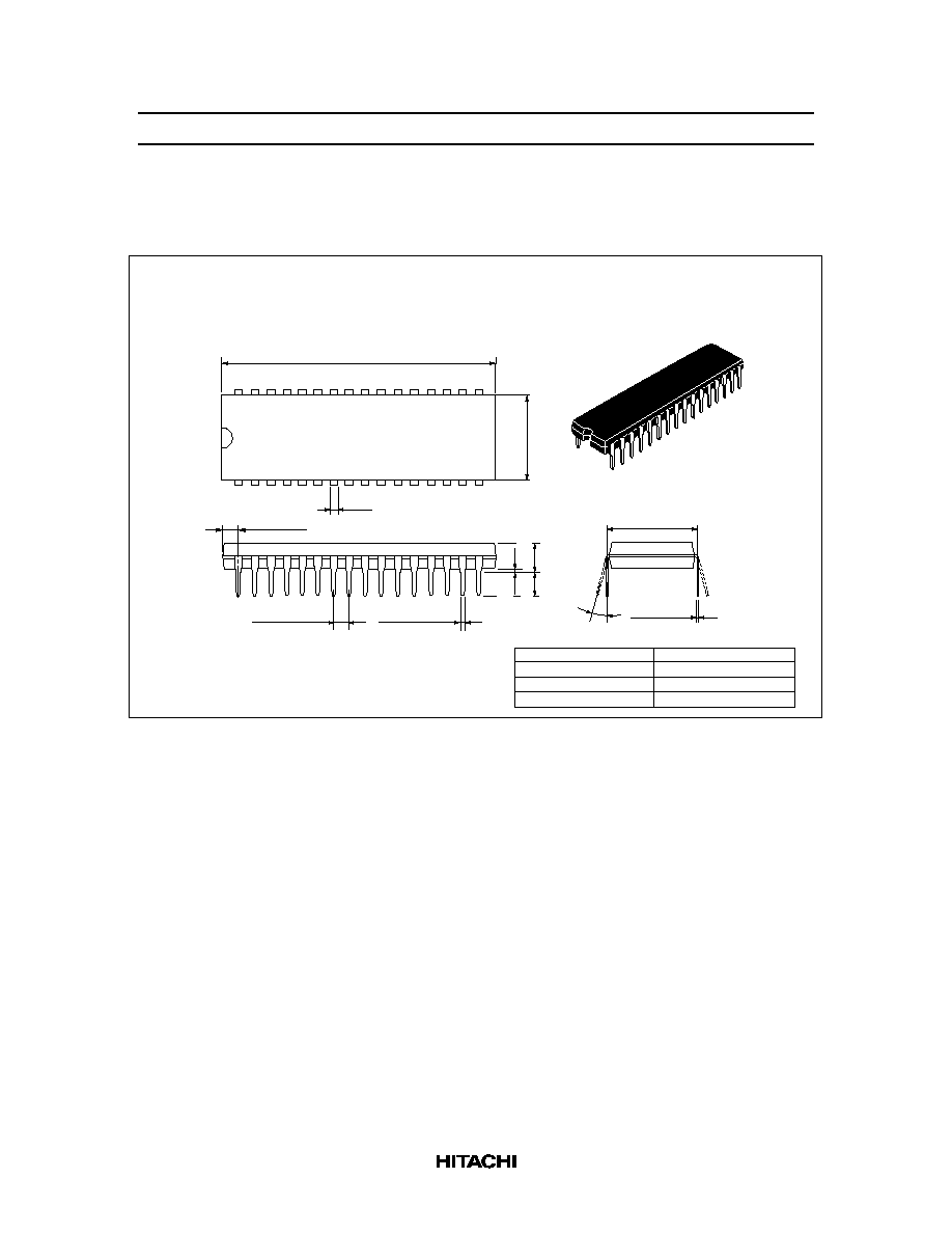
Package Dimensions
HM658512ALP Series (DP-32)
0.51 Min
2.54 Min
5.08 Max
0.25
+ 0.11
0.05
2.54
±
0.25
0.48
±
0.10
0
°
15
°
41.90
42.50 Max
13.4
13.7 Max
15.24
32
17
1
16
2.30 Max
1.20
Hitachi Code
JEDEC
EIAJ
Weight (reference value)
DP-32
--
Conforms
5.1 g
Unit: mm
HM658512A Series
19
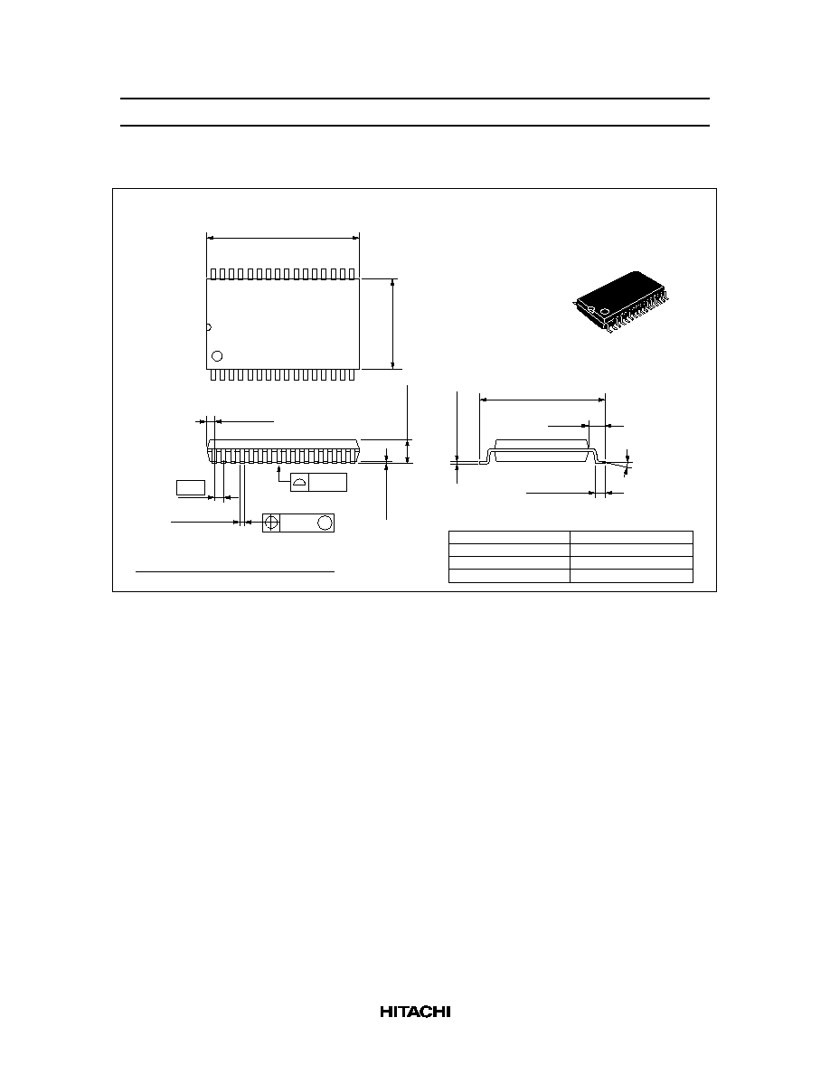
HM658512ALFP Series (FP-32D)
0.15
M
0.40
±
0.08
20.45
1.00 Max
1.27
11.30
1.42
3.00 Max
0.22
±
0.05
20.95 Max
32
17
1
16
0
°
8
°
0.80
±
0.20
14.14
±
0.30
0.10
Hitachi Code
JEDEC
EIAJ
Weight (reference value)
FP-32D
Conforms
--
1.3 g
0.38
±
0.06
+ 0.12
0.10
0.15
0.20
±
0.04
Unit: mm
Dimension including the plating thickness
Base material dimension
HM658512A Series
20
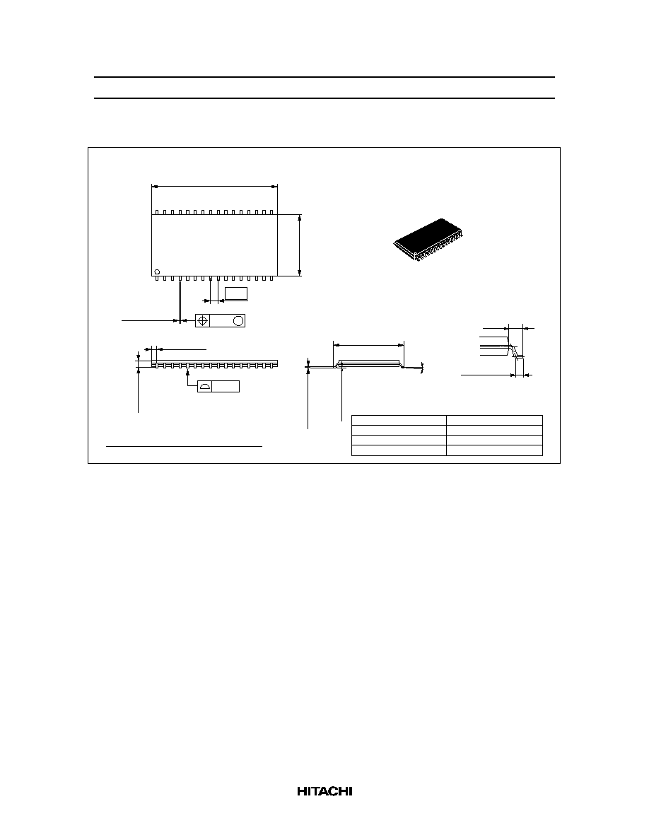
HM658512ALTT Series (TTP-32D)
1.27
0.21
M
0.42
±
0.08
0.10
10.16
20.95
21.35 Max
17
16
32
1
1.20 Max
0
°
5
°
0.13
±
0.05
0.17
±
0.05
11.76
±
0.20
0.50
±
0.10
1.15 Max
0.80
Hitachi Code
JEDEC
EIAJ
Weight (reference value)
TTP-32D
Conforms
--
0.51 g
0.40
±
0.06
0.125
±
0.04
Unit: mm
Dimension including the plating thickness
Base material dimension
HM658512A Series
21
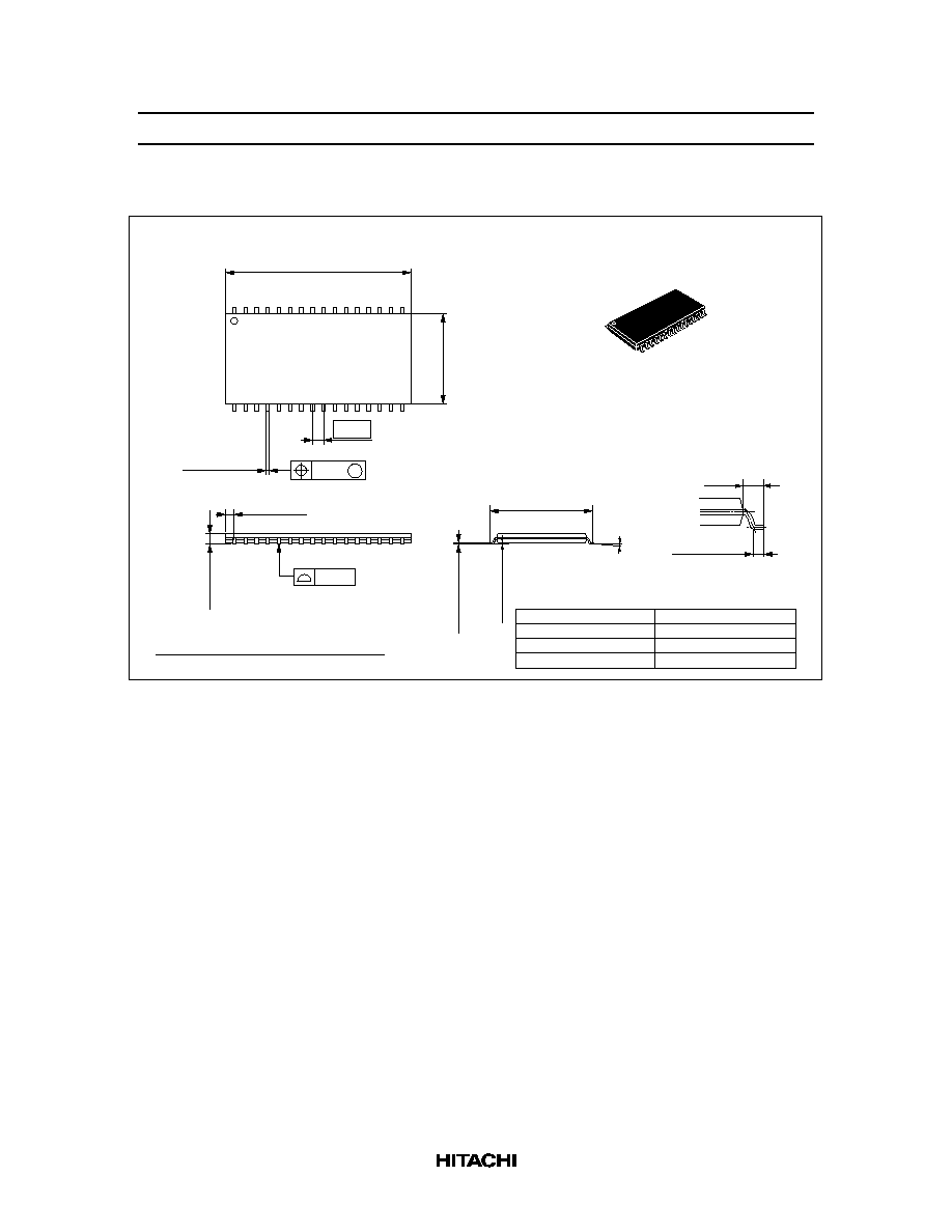
HM658512ALRR Series (TTP-32DR)
1.27
0.21
M
0.42
±
0.08
0.10
10.16
20.95
21.35 Max
16
17
1
32
1.20 Max
0
°
5
°
0.13
±
0.05
0.17
±
0.05
11.76
±
0.20
0.50
±
0.10
1.15 Max
0.80
Hitachi Code
JEDEC
EIAJ
Weight (reference value)
TTP-32DR
Conforms
--
0.51 g
0.40
±
0.06
0.125
±
0.04
Unit: mm
Dimension including the plating thickness
Base material dimension

HM658512A Series
22
When using this document, keep the following in mind:
1. This document may, wholly or partially, be subject to change without notice.
2. All rights are reserved: No one is permitted to reproduce or duplicate, in any form, the whole or part of
this document without Hitachi's permission.
3. Hitachi will not be held responsible for any damage to the user that may result from accidents or any
other reasons during operation of the user's unit according to this document.
4. Circuitry and other examples described herein are meant merely to indicate the characteristics and
performance of Hitachi's semiconductor products. Hitachi assumes no responsibility for any intellectual
property claims or other problems that may result from applications based on the examples described
herein.
5. No license is granted by implication or otherwise under any patents or other rights of any third party or
Hitachi, Ltd.
6. MEDICAL APPLICATIONS: Hitachi's products are not authorized for use in MEDICAL
APPLICATIONS without the written consent of the appropriate officer of Hitachi's sales company.
Such use includes, but is not limited to, use in life support systems. Buyers of Hitachi's products are
requested to notify the relevant Hitachi sales offices when planning to use the products in MEDICAL
APPLICATIONS.
Hitachi, Ltd.
Semiconductor & IC Div.
Nippon Bldg., 2-6-2, Ohte-machi, Chiyoda-ku, Tokyo 100-0004, Japan
Tel: Tokyo (03) 3270-2111
Fax: (03) 3270-5109
For further information write to:
Hitachi Semiconductor
(America) Inc.
2000 Sierra Point Parkway
Brisbane, CA. 94005-1897
U S A
Tel: 800-285-1601
Fax:303-297-0447
Hitachi Europe GmbH
Continental Europe
Dornacher Straße 3
D-85622 Feldkirchen
München
Tel: 089-9 91 80-0
Fax: 089-9 29 30-00
Hitachi Europe Ltd.
Electronic Components Div.
Northern Europe Headquarters
Whitebrook Park
Lower Cookham Road
Maidenhead
Berkshire SL6 8YA
United Kingdom
Tel: 01628-585000
Fax: 01628-585160
Hitachi Asia Pte. Ltd.
16 Collyer Quay #20-00
Hitachi Tower
Singapore 049318
Tel: 535-2100
Fax: 535-1533
Hitachi Asia (Hong Kong) Ltd.
Unit 706, North Tower,
World Finance Centre,
Harbour City, Canton Road
Tsim Sha Tsui, Kowloon
Hong Kong
Tel: 27359218
Fax: 27306071
Copyright © Hitachi, Ltd., 1998. All rights reserved. Printed in Japan.
Document Outline
- Description
- Features
- Ordering Information
- Pin Arrangement
- Pin Description
- Block Diagram
- Pin Functions
- Refresh
- Notes on Using the HM658512A
- Function Table
- Absolute Maximum Ratings
- Recommended DC Operating Conditions
- DC Characteristics
- Capacitance
- AC Characteristics
- Timing Waveform
- Read Cycle
- Write Cycle (1) (OE high)
- Write Cycle (2) (OE low)
- Read-Modify-Write Cycle
- Automatic Refresh Cycle
- Self Refresh Cycle
- Low V CC Data Retention Characteristics
- Low VCC Data Retention Timing Waveform
- Package Dimensions
- HM658512ALP Series (DP-32)
- HM658512ALFP Series (FP-32D)
- HM658512ALTT Series (TTP-32D)
- HM658512ALRR Series (TTP-32DR)