 | –≠–ª–µ–∫—Ç—Ä–æ–Ω–Ω—ã–π –∫–æ–º–ø–æ–Ω–µ–Ω—Ç: HMC262 | –°–∫–∞—á–∞—Ç—å:  PDF PDF  ZIP ZIP |
1 - 16
12 Elizabeth Drive, Chelmsford, MA 01824 Phone: 978-250-3343
Fax: 978-250-3373
Web Site: www.hittite.com
MICROWAVE CORPORATION
F
EBRUARY
2001
A
MPLIFIERS
1
DIE
Features
EXCELLENT NOISE FIGURE : 2 dB
STABLE GAIN VS TEMPERATURE: 25 dB ±1.5 dB
SINGLE SUPPLY : +3V@ 36mA
SMALL SIZE: 1.32 mm x 2.08 mm
The HMC262 chip is a GaAs MMIC Low Noise
Amplifier (LNA) which covers the frequency
range of 15 to 24 GHz. The chip can easily be
integrated into Multi-Chip Modules (MCMs) due
to its small (2.75 mm
2
) size. The chip utilizes a
GaAs PHEMT process offering 25 dB gain from
a single bias supply of + 3V @ 36 mA with a
noise figure of 2 dB. This LNA can be used in
microwave & millimeter wave point-to-point ra-
dios, VSAT, and other SATCOM applications.
All data is with the chip in a 50 ohm test fixture
connected via 0.025 mm (1 mil) diameter wire
bonds of minimal length 0.31 mm (<12 mils). The
HMC262 may be used in conjunction with
HMC203, HMC258, HMC264, or HMC265 mix-
ers to realize a microwave or millimeterwave
system receiver.
General Description
Guaranteed Performance,
Vdd = +3V, -55 to +85 deg C
r
e
t
e
m
a
r
a
P
.
n
i
M
.
p
y
T
.
x
a
M
.
n
i
M
.
p
y
T
.
x
a
M
.
n
i
M
.
p
y
T
.
x
a
M
s
t
i
n
U
e
g
n
a
R
y
c
n
e
u
q
e
r
F
7
1
-
5
1
0
2
-
7
1
4
2
-
0
2
z
H
G
n
i
a
G
9
1
4
2
9
1
5
2
5
1
0
2
B
d
e
r
u
g
i
F
e
s
i
o
N
8
.
2
0
.
5
0
.
2
7
.
3
2
.
2
9
.
3
B
d
s
s
o
L
n
r
u
t
e
R
t
u
p
n
I
5
4
0
1
6
2
1
B
d
s
s
o
L
n
r
u
t
e
R
t
u
p
t
u
O
7
6
1
5
2
1
6
B
d
n
o
i
t
a
l
o
s
I
e
s
r
e
v
e
R
9
3
5
4
7
3
2
4
5
3
0
4
B
d
)
B
d
1
P
(
n
o
i
s
s
e
r
p
m
o
C
B
d
1
r
o
f
r
e
w
o
P
t
u
p
t
u
O
1
-
3
1
5
.
4
0
4
m
B
d
)
t
a
s
P
(
r
e
w
o
P
t
u
p
t
u
O
d
e
t
a
r
u
t
a
S
3
8
4
8
2
6
m
B
d
)
3
P
I
(
t
p
e
c
r
e
t
n
I
r
e
d
r
O
d
r
i
h
T
t
u
p
t
u
O
8
3
1
9
3
1
6
0
1
m
B
d
)
d
d
V
(
e
g
a
t
l
o
V
y
l
p
p
u
S
5
7
.
2
0
.
3
5
2
.
3
5
7
.
2
0
.
3
5
2
.
3
5
7
.
2
0
.
3
5
2
.
3
c
d
V
)
V
3
+
=
d
d
V
(
)
d
d
I
(
t
n
e
r
r
u
C
y
l
p
p
u
S
6
3
8
4
6
3
8
4
6
3
8
4
A
m
GaAs MMIC LOW NOISE AMPLIFIER 15 - 24 GHz
HMC262
V
01.05.00
1 - 17
12 Elizabeth Drive, Chelmsford, MA 01824 Phone: 978-250-3343
Fax: 978-250-3373
Web Site: www.hittite.com
MICROWAVE CORPORATION
F
EBRUARY
2001
1
A
MPLIFIERS
DIE
HMC262 LOW NOISE AMPLIFIER 15 - 24 GHz
0
5
10
15
20
25
30
-30
-25
-20
-15
-10
-5
0
14
16
18
20
22
24
GA
IN
(d
B
m
)
RET
URN
LO
SS
(
d
B)
FREQUENCY (GHz)
GAIN
S22(Output)
S11(Input)
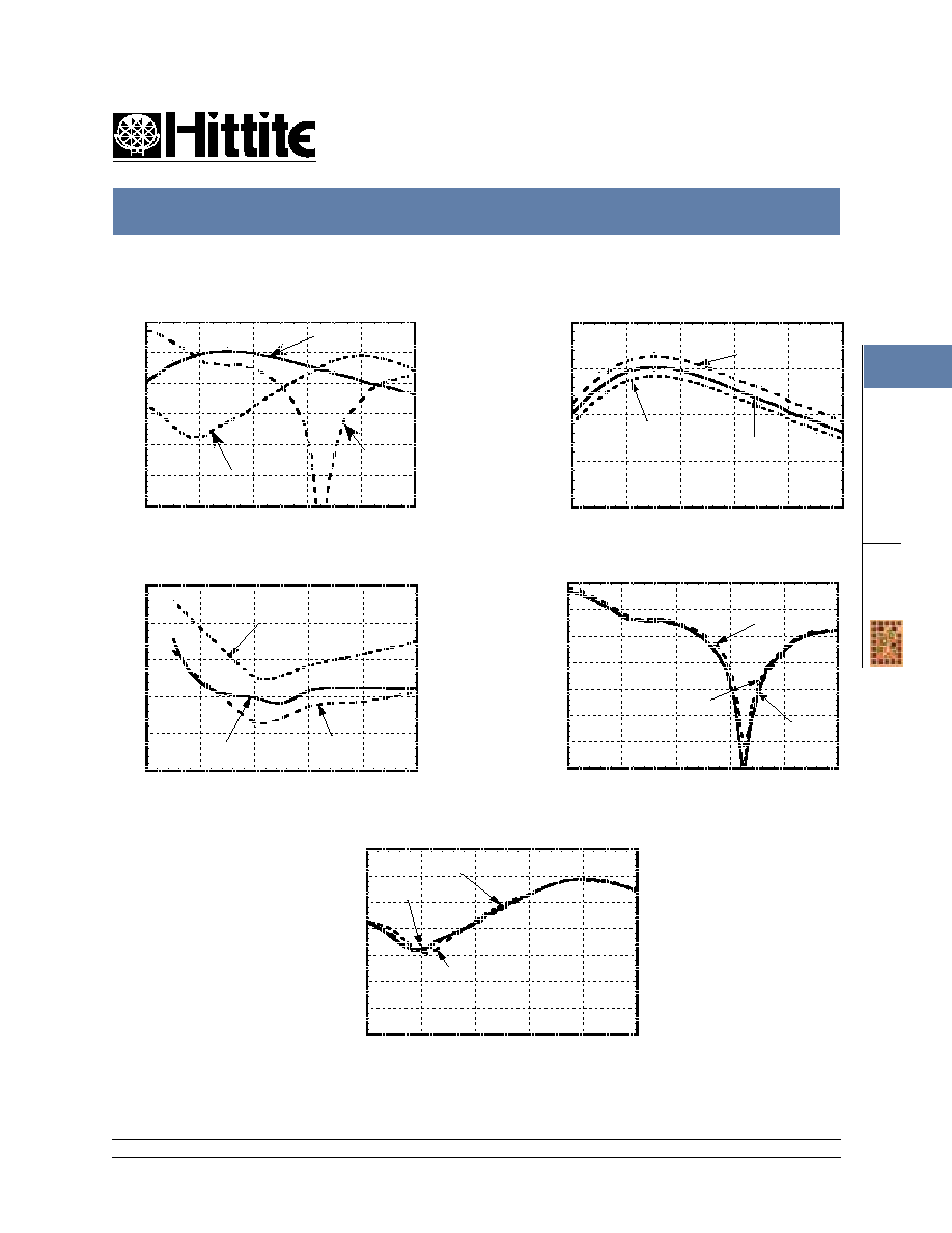
Broadband Gain and Return Loss
Input Return Loss
Gain vs. Temperature
-35
-30
-25
-20
-15
-10
-5
0
14
16
18
20
22
24
I
N
PUT
R
ETURN
LOSS
(
d
B)
FREQUENCY (GHz)
-55 C
+25 C
+85 C
-35
-30
-25
-20
-15
-10
-5
0
14
16
18
20
22
24
OUTPUT
RETURN
L
O
SS
(
d
B)
FREQUENCY (GHz)
-55 C
+25 C
+85 C
Output Return Loss
0
1
2
3
4
5
14
16
18
20
22
24
NOI
S
E
F
I
G
URE
(
d
B)
FREQUENCY (GHz)
+85 C
-55 C
+25 C
Noise Figure
10
15
20
25
30
14
16
18
20
22
24
GAIN
(
d
B)
FREQUENCY (GHz)
+85 C
-55 C
+25 C
All data is with the chip in a 50 ohm test fixture connected via 0.025 mm (1 mil) diameter wire bonds of minimal
length 0.31 mm (<12 mils).
HMC262
V
01.05.00
1 - 18
12 Elizabeth Drive, Chelmsford, MA 01824 Phone: 978-250-3343
Fax: 978-250-3373
Web Site: www.hittite.com
MICROWAVE CORPORATION
F
EBRUARY
2001
A
MPLIFIERS
1
DIE
HMC262 LOW NOISE AMPLIFIER 15 - 24 GHz
0
5
10
15
20
14
16
18
20
22
24
IP
3
(
dB
m
)
FREQUENCY (GHz)
+85 C
-55 C
+25 C
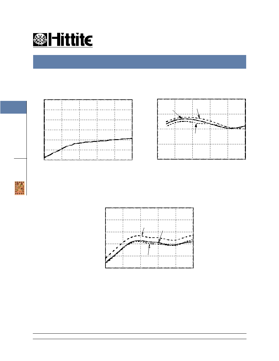
IP3 Output @ Vdd = +3V
0
2
4
6
8
10
14
16
18
20
22
24
P
1dB
(dB
m
)
FREQUENCY (GHz)
+85C
+25C
-55C
P1dB Output @ Vdd = +3V
-60
-50
-40
-30
-20
-10
0
14
16
18
20
22
24
IS
OLA
T
ION
(
dB
)
FREQUENCY (GHz)
Isolation
All data is with the chip in a 50 ohm test fixture connected via 0.025 mm (1 mil) diameter wire bonds of minimal
length 0.31 mm (<12 mils).
HMC262
V
01.05.00
1 - 19
12 Elizabeth Drive, Chelmsford, MA 01824 Phone: 978-250-3343
Fax: 978-250-3373
Web Site: www.hittite.com
MICROWAVE CORPORATION
F
EBRUARY
2001
1
A
MPLIFIERS
DIE
HMC262 LOW NOISE AMPLIFIER 15 - 24 GHz
Absolute Maximum Ratings
)
d
d
V
(
e
g
a
t
l
o
V
y
l
p
p
u
S
)
3
V
=
2
V
=
1
V
=
d
d
V
(
c
d
V
5
.
5
+
)
V
3
+
=
d
d
V
(
)
n
i
F
R
(
r
e
w
o
P
t
u
p
n
I
m
B
d
5
-
)
c
T
(
e
r
u
t
a
r
e
p
m
e
T
l
e
n
n
a
h
C
C
∞
5
7
1
)
c
j
(
e
c
n
a
t
s
i
s
e
R
l
a
m
r
e
h
T
)
e
d
i
s
k
c
a
B
l
e
n
n
a
h
C
(
W
/
C
∞
0
9
e
r
u
t
a
r
e
p
m
e
T
e
g
a
r
o
t
S
C
∞
0
5
1
+
o
t
5
6
-
e
r
u
t
a
r
e
p
m
e
T
g
n
i
t
a
r
e
p
O
C
∞
5
8
+
o
t
5
5
-
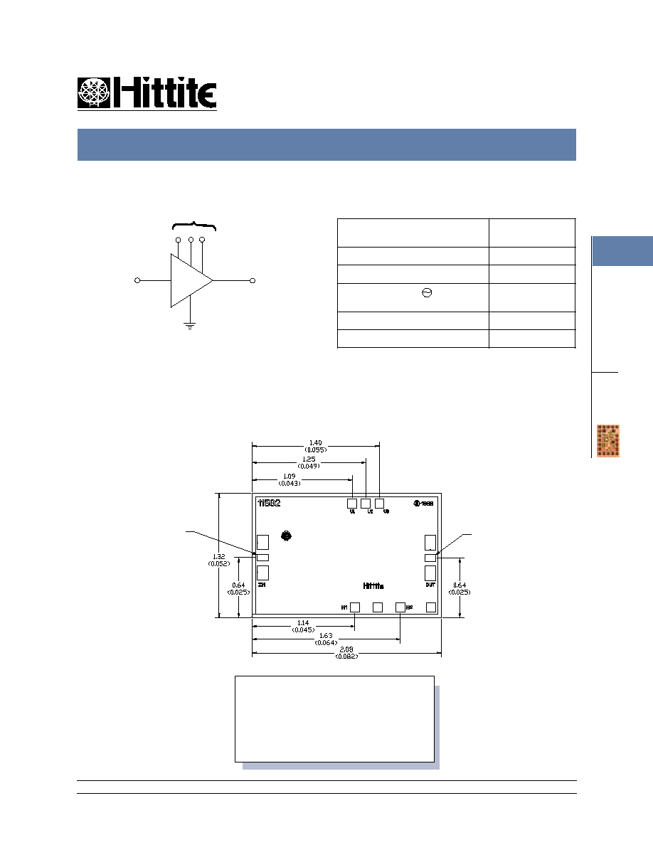
Outline
( See Die Handling, Mounting, Bonding Note Page 1 - 13 )
RF OUT
RF IN
Vdd
(+3V to +5V)
Ground
(Backside)
V1
V3
V2
ALL DIMENSION IN MILLIMETERS (INCHES)
ALL TOLERANCES ARE ±0.025 (0.001)
DIE THICKNESS IS 0.100 (0.004) BACKSIDE IS GROUND
BOND PADS ARE 0.100 (0.004) SQUARE
BOND PAD SPACING, CTR-CTR: 0.150 (0.006)
BACKSIDE METALLIZATION : GOLD
BOND PAD METALLIZATION : GOLD
NOTE: Connect V1, V2, & V3 to Vdd via a 100pF single layer chip bypass capacitor. Place the
capacitor no further than 0.762 mm (30mils) from the HMC262. M1 & M2 are to remain open circuit
(no connection).
Schematic
RF IN
RF OUT
HMC262
V
01.05.00
1 - 20
12 Elizabeth Drive, Chelmsford, MA 01824 Phone: 978-250-3343
Fax: 978-250-3373
Web Site: www.hittite.com
MICROWAVE CORPORATION
F
EBRUARY
2001
A
MPLIFIERS
1
DIE
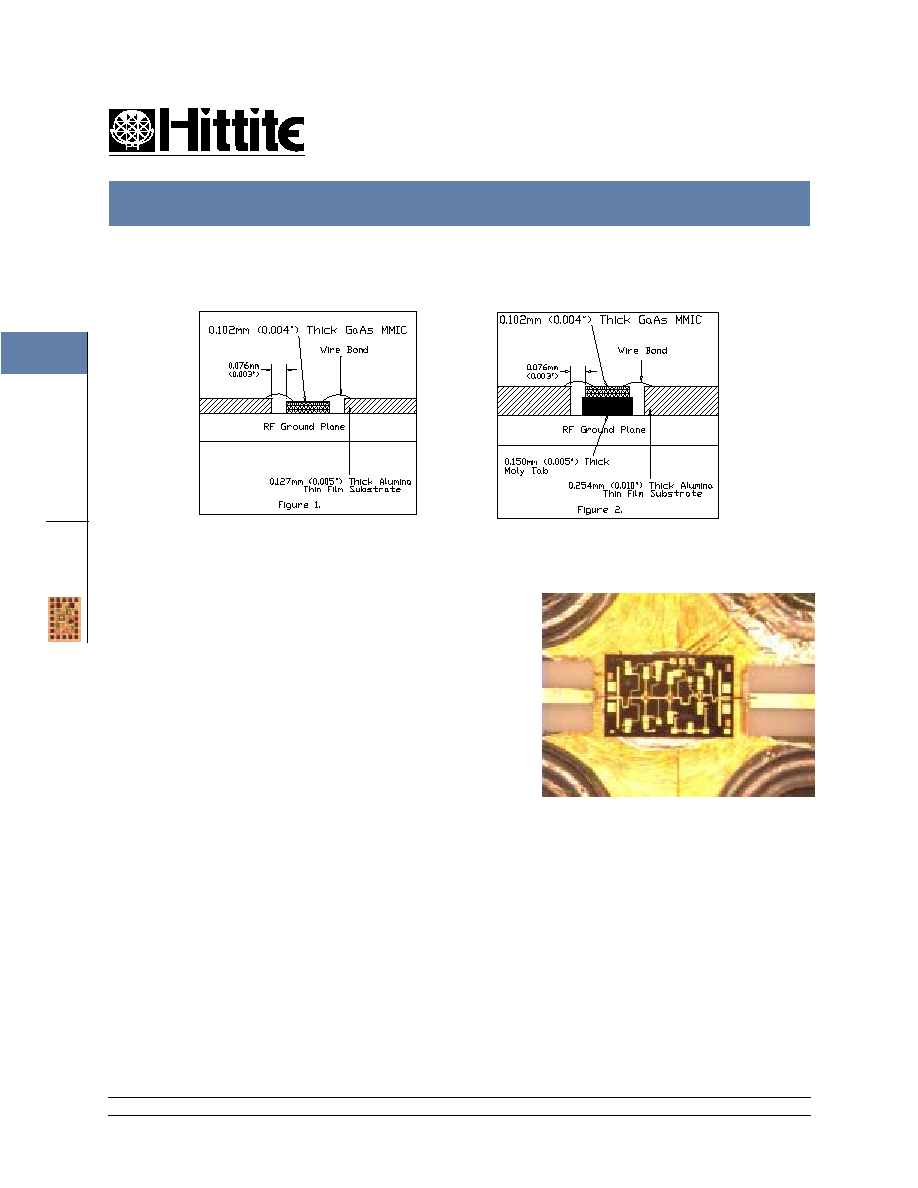
MIC Assembly Techniques for HMC262
HMC262 LOW NOISE AMPLIFIER 15 - 24 GHz
Mounting & Bonding Techniques for Millimeterwave GaAs MMICs
The die should be attached directly to the ground plane eutectically or
with conductive epoxy (see HMC general Handling, Mounting, Bond-
ing Note).
50 Ohm Microstrip transmission lines on 0.127mm (5 mil) thick alumina
thin film substrates are recommended for bringing RF to and from the
chip (Figure 1). If 0.254mm (10 mil) thick alumina thin film substrates
must be used, the die should be raised 0.150mm (6 mils) so that the
surface of the die is coplanar with the surface of the substrate. One way
to accomplish this is to attach the 0.102mm (4 mil) thick die to a
0.150mm (6 mil) thick molybdenum heat spreader (moly-tab) which is
then attached to the ground plane (Figure 2).
Microstrip substrates should brought as close to the die as possible in
order to minimize bond wire length. Typical die-to-substrate spacing
is 0.076mm (3 mils).
An RF bypass capacitor should be used on the Vdd input. A 100 pF single layer capacitor (mounted eutectically or by
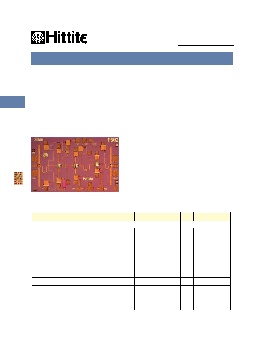
conductive epoxy) placed no further than 0.762mm (30 Mils) from the chip is recommended. The photo in figure 3 shows
a typical assembly for the HMC262 MMIC chip.
Figure 3: Typical HMC262 Assembly
HMC262
V
01.05.00