 | –≠–ª–µ–∫—Ç—Ä–æ–Ω–Ω—ã–π –∫–æ–º–ø–æ–Ω–µ–Ω—Ç: HMC283LM1 | –°–∫–∞—á–∞—Ç—å:  PDF PDF  ZIP ZIP |

MICROWAVE CORPORATION
8 - 14
For price, delivery, and to place orders, please contact Hittite Microwave Corporation:
12 Elizabeth Drive, Chelmsford, MA 01824 Phone: 978-250-3343 Fax: 978-250-3373
Order Online at www.hittite.com
AMPLIFIERS - SMT
8
HMC283LM1
SMT MEDIUM POWER GaAs MMIC
AMPLIFIER, 17 - 40 GHz
v04.1201
General Description
Features
Functional Diagram
SMT mmWave Package
Psat Output Power: +21 dBm
High Gain: 21 dB
No External Matching Required
Electrical Specifi cations,
T
A
= +25∞ C, Vdd= +3.5V*, ldd = 300 mA
Typical Applications
The HMC283LM1 is a Medium Power Amplifi er (MPA)
in a SMT leadless chip carrier package covering 17 to
40 GHz. The LM1 is a true surface mount broadband
millimeterwave package offering low loss & excellent
I/O match preserving MMIC chip performance. Utilizing
a GaAs PHEMT process, the device offers 20 dB gain
and +21 dBm ouput power from a bias supply of +3.5V
@ 300mA. As an alternative to chip-and-wire hybrid
assemblies the HMC283LM1 eliminates the need for
wirebonding, thereby providing a consistent connec-
tion interface for the customer. The amplifi er may be
used as a frequency doubler. A built-in-test pad (Vdet)
allows monitoring of microwave output power. All data
is with the non-hermetic, epoxy sealed LM1 packaged
MPA device mounted in a 50 ohm test fi xture.
The HMC283LM1 is ideal for:
∑ Millimeterwave Point-to-Point Radios
∑ LMDS
∑ SATCOM
Parameter
Min.
Typ.
Max.
Min.
Typ.
Max.
Units
Frequency Range
17 - 40
21 - 30
GHz
Gain
15
20
17
22
dB
Gain Variation over Temperature
0.05
0.07
0.05
0.07
dB/∞C
Input Return Loss
6
10
6
12
dB
Output Return Loss
4
7
4
8
dB
Reverse Isolation
30
40
35
45
dB
Output Power for 1 dB Compression (P1dB)
14
18
14
18
dBm
Saturated Output Power (Psat)
17
21
17
21
dBm
Output Third Order Intercept (IP3)
22
27
21
27
dBm
Noise Figure
10
10
dB
Supply Current (Idd)
300
330
300
330
mA
*Vdd = +3.5V, adjust Vgg = Vgg1, Vgg2 between -2.0 to +0.4V to achieve Idd = 300 mA typical.
MICROWAVE CORPORATION
8 - 15
For price, delivery, and to place orders, please contact Hittite Microwave Corporation:
12 Elizabeth Drive, Chelmsford, MA 01824 Phone: 978-250-3343 Fax: 978-250-3373
Order Online at www.hittite.com
AMPLIFIERS - SMT
8
-25
-20
-15
-10
-5
0
5
10
15
20
25
30
10
15
20
25
30
35
40
S11
S21
S22
RESPONSE (dB)
FREQUENCY (GHz)
0
5
10
15
20
25
30
16
18
20
22
24
26
28
30
32
34
36
38
40
42
+25C
+85C
-40C
GAIN (dB)
FREQUENCY (GHz)
-60
-50
-40
-30
-20
-10
0
16
18
20
22
24
26
28
30
32
34
36
38
40
42
+25C
+85C
-40C
REVERSE ISOLATION (dB)
FREQUENCY (GHz)
-25
-20
-15
-10
-5
0
16
18
20
22
24
26
28
30
32
34
36
38
40
42
+25C
+85C
-40C
INPUT RETURN LOSS (dB)
FREQUENCY (GHz)
HMC283LM1
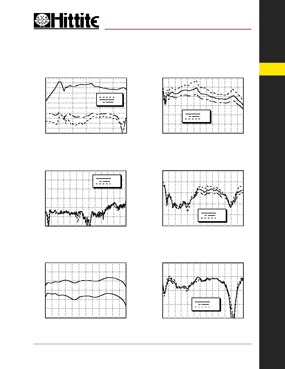
Reverse Isolation vs. Temperature
Input Return Loss vs. Temperature
Broadband Gain & Return Loss
Gain vs. Temperature
P1dB and Psat @ 25 ∞C
13
15
17
19
21
23
25
16
18
20
22
24
26
28
30
32
34
36
38
40
OUTPUT P1dB & Psat (dBm)
FREQUENCY (GHz)
Psat
P1dB
Output Return Loss vs. Temperature
-20
-15
-10
-5
0
16
18
20
22
24
26
28
30
32
34
36
38
40
42
+25C
+85C
-40C
OUTPUT RETURN LOSS (dB)
FREQUENCY (GHz)
SMT MEDIUM POWER GaAs MMIC
AMPLIFIER, 17 - 40 GHz
v04.1201

MICROWAVE CORPORATION
8 - 16
For price, delivery, and to place orders, please contact Hittite Microwave Corporation:
12 Elizabeth Drive, Chelmsford, MA 01824 Phone: 978-250-3343 Fax: 978-250-3373
Order Online at www.hittite.com
AMPLIFIERS - SMT
8
HMC283LM1
P1dB vs. Temperature
Psat vs. Temperature
Power Compression @ 20 GHz
13
15
17
19
21
23
25
16
18
20
22
24
26
28
30
32
34
36
38
40
OUTPUT P1dB (dBm)
FREQUENCY (GHz)
FREQUENCY (GHz)
-40 C
+25 C
+85C
Output IP3 vs. Temperature
Power Compression @ 28 GHz
Power Compression @ 39 GHz
0
2
4
6
8
10
12
14
16
18
20
22
24
-10
-8
-6
-4
-2
0
2
4
6
8
10
Pout (dBm), GAIN (dB), PAE (%)
INPUT POWER (dBm)
Pout
PAE
Gain
0
2
4
6
8
10
12
14
16
18
20
22
24
-10
-8
-6
-4
-2
0
2
4
6
8
10
Pout (dBm), GAIN (dB), PAE (%)
INPUT POWER (dBm)
Pout
PAE
Gain
13
15
17
19
21
23
25
16
18
20
22
24
26
28
30
32
34
36
38
40
Psat (dBm)
FREQUENCY (GHz)
-40 C
+25 C
+85C
0
2
4
6
8
10
12
14
16
18
20
22
24
-10
-8
-6
-4
-2
0
2
4
6
8
10
Pout (dBm), GAIN (dB), PAE (%)
INPUT POWER (dBm)
Pout
PAE
Gain
SMT MEDIUM POWER GaAs MMIC
AMPLIFIER, 17 - 40 GHz
v04.1201
Frequency (GHz)
Temperature
20
28
38
-40 ∞C
29.0
28.0
31.0
+25 ∞C
28.5
27.5
28.5
+85 ∞C
27.5
26.0
24.5
All levels in dBm

MICROWAVE CORPORATION
8 - 17
For price, delivery, and to place orders, please contact Hittite Microwave Corporation:
12 Elizabeth Drive, Chelmsford, MA 01824 Phone: 978-250-3343 Fax: 978-250-3373
Order Online at www.hittite.com
AMPLIFIERS - SMT
8
HMC283LM1
Outline Drawing
Absolute Maximum Ratings
SMT MEDIUM POWER GaAs MMIC
AMPLIFIER, 17 - 40 GHz
v04.1201
NOTES:
1. MATERIAL: PLASTIC
2. PLATING: GOLD OVER NICKEL
3. DIMENSIONS ARE IN INCHES [MILLIMETERS].
4. ALL TOLERANCES ARE ± 0.005 [± 0.13].
5. ALL GROUNDS MUST BE SOLDERED TO PCB RF GROUND.
6.
∑
INDICATES PIN 1
Drain Bias Voltage (Vdd)
+5.0 Vdc
Drain Bias Current (Idd)
400 mA
Gate Bias Voltage (Vgg1, Vgg2)
-2.0 to +0.4 Vdc
Gate Bias Current (Igg)
4.0 mA
RF Input Power (RFin)(Vdd = +3.5 Vdc)
+10 dBm
Channel Temperature
175 ∞C
Continuous Pdiss (T = 85 ∞C)
(derate 16 mW/∞C above 85 ∞C)
1.44 W
Thermal Resistance
(channel to ground paddle)
62.5 ∞C/W
Storage Temperature
-65 to +150 ∞C
Operating Temperature
-40 to +85 ∞C
Pin
Function
1
GND
2
Vdd
3
GND
4
RF OUT
5
VDET
6
Vgg2
7
Vgg1
8
RF IN

MICROWAVE CORPORATION
8 - 18
For price, delivery, and to place orders, please contact Hittite Microwave Corporation:
12 Elizabeth Drive, Chelmsford, MA 01824 Phone: 978-250-3343 Fax: 978-250-3373
Order Online at www.hittite.com
AMPLIFIERS - SMT
8
HMC283LM1
Evaluation PCB
The grounded Co-Planar Wave Guide (CPWG) PCB input/output transitions allow use of Ground-Signal-Ground (GSG)
probes for testing. Suggested probe pitch is 400um (16 mils). Alternatively, the board can be mounted in a metal hous-
ing with 2.4 mm coaxial connectors.
Evaluation Circuit Board Layout Design Details
LM1 Evaluation PCB
LM1 Package Mounted to Evaluation PCB
SMT MEDIUM POWER GaAs MMIC
AMPLIFIER, 17 - 40 GHz
v04.1201
Layout Technique
Micro Strip to CPWG
Material
Rogers 4003 with 1/2 oz. Cu
Dielectric Thickness
0.008" (0.20 mm)
Microstrip Line Width
0.018" (0.46 mm)
CPWG Line Width
0.016" (0.41 mm)
CPWG Line to GND Gap
0.005" (0.13 mm)
Ground Via Hole Diameter
0.008" (0.20 mm)
C1
100 pF Capacitor, 0402 Pkg.
C2
33,000 pF Capacitor, 1206 Pkg.
R1
1,000 Ohm Resistor, 0402 Pkg.
R2
100 Ohm Resistor, 0402 Pkg.

MICROWAVE CORPORATION
8 - 19
For price, delivery, and to place orders, please contact Hittite Microwave Corporation:
12 Elizabeth Drive, Chelmsford, MA 01824 Phone: 978-250-3343 Fax: 978-250-3373
Order Online at www.hittite.com
AMPLIFIERS - SMT
8
Suggested LM1 PCB Land Pattern
Tolerance: ± 0.003" (± 0.08 mm)
HMC283LM1
Amplifi er Application Circuit
SMT MEDIUM POWER GaAs MMIC
AMPLIFIER, 17 - 40 GHz
Note: Vgg1 and Vgg2 may be connected to a common Vgg feed. For optimal stable operation, it is recommended that
a voltage divider network be employed as shown above with Vgg set to achieve ldd = 300 mA typical.
v04.1201
Recommended Component Values
C1
100 pF
C2
33,000 pF
R1
1,000 Ohm
R2
100 Ohm

MICROWAVE CORPORATION
8 - 20
For price, delivery, and to place orders, please contact Hittite Microwave Corporation:
12 Elizabeth Drive, Chelmsford, MA 01824 Phone: 978-250-3343 Fax: 978-250-3373
Order Online at www.hittite.com
AMPLIFIERS - SMT
8
The HMC LM1 package was designed to be compatible with high volume surface mount PCB assembly processes.
The LM1 package requires a specifi c mounting pattern to
allow proper mechanical attachment and to optimize electrical
performance at millimeterwave frequencies. The PCB layout
pattern can be found on each LM1 product data sheet. It can
also be provided as an electronic drawing upon request from
Hittite Sales & Application Engineering.
Follow these precautions to avoid permanent damage:
Cleanliness: Observe proper handling procedures to ensure
clean devices and PCBs. LM1 devices should remain in their
original packaging until component placement to ensure no
contamination or damage to RF, DC & ground contact areas.
Static Sensitivity: Follow ESD precautions to protect against
ESD strikes.
General Handling: Handle the LM1 package on the top with a
vacuum collet or along the edges with a sharp pair of bent tweezers. Avoid damaging the RF, DC, & ground contacts
on the package bottom. Do not apply excess pressure to the top of the lid.
Solder Materials & Temperature Profi le: Follow the information contained in the application note. Hand soldering is
not recommended. Conductive epoxy attachment is not recommended.
Solder Paste
Solder paste should be selected based on the user's experience and should be compatible with the metallization
systems used. See the LM1 data sheet Outline drawing for pin & ground contact metallization schemes.
Solder Paste Application
Solder paste is generally applied to the PCB using either a stencil printer or dot placement. The volume of solder
paste will be dependent on PCB and component layout and should be controlled to ensure consistent mechanical &
electrical performance. Excess solder may create unwanted electrical parasitics at high frequencies.
Solder Refl ow
The soldering process is usually accomplished in a refl ow oven but may also use a vapor phase process. A solder
refl ow profi le is suggested above.
Prior to refl owing product, temperature profi les should be measured using the same mass as the actual assemblies.
The thermocouple should be moved to various positions on the board to account for edge and corner effects and
varying component masses. The fi nal profi le should be determined by mounting the thermocouple to the PCB at the
location of the device.
Follow solder paste and oven vendor's recommendations when developing a solder refl ow profi le. A standard profi le
will have a steady ramp up from room temperature to the pre-heat temperature to avoid damage due to thermal
shock. Allow enough time between reaching pre-heat temperature and refl ow for the solvent in the paste to evaporate
and the fl ux to completely activate. Refl ow must then occur prior to the fl ux being completely driven off. The duration
of peak refl ow temperature should not exceed 15 seconds. Packages have been qualifi ed to withstand a peak
temperature of 235
0
C for 15 seconds. Verify that the profi le will not expose the device to temperatures in excess of
235
0
C.
Cleaning
A water-based fl ux wash may be used.
Recommended SMT Attachment Technique
Preparation & Handling of the LM1 Millimeterwave Package for Surface Mounting
HMC283LM1
SMT MEDIUM POWER GaAs MMIC
AMPLIFIER, 17 - 40 GHz
25
50
75
100
125
150
175
200
225
0
1
2
3
4
5
6
7
8
TEMPERATURE (
0
C)
TIME (min)
Recommended solder reflow profile
for HMC LM1 SMT package
v04.1201

MICROWAVE CORPORATION
8 - 21
For price, delivery, and to place orders, please contact Hittite Microwave Corporation:
12 Elizabeth Drive, Chelmsford, MA 01824 Phone: 978-250-3343 Fax: 978-250-3373
Order Online at www.hittite.com
AMPLIFIERS - SMT
8
Alternate Applications:
Frequency Multiplier Performance
Voltage Detector, Built-In-Test (B.I.T.)
HMC283LM1
SMT MEDIUM POWER GaAs
AMPLIFIER, 17 - 40 GHz
-10
-9
-8
-7
-6
-5
-4
-3
-2
-1
0
1
2
3
4
5
10
15
20
25
30
35
40
CONVERSION LOSS (dB)
OUTPUT FREQUENCY (GHz)
15 dBm
10 dBm
18 dBm
0
0.2
0.4
0.6
0.8
1
1.2
1.4
1.6
1.8
2
10
12
14
16
18
20
22
DETECTED VOLTAGE
INTO 10K RESISTOR (Volts)
OUTPUT POWER (dBm)
18 GHz
38 GHz
28 GHz
22 GHz
0
0.2
0.4
0.6
0.8
1
1.2
1.4
1.6
10
12
14
16
18
20
22
DETECTED VOLTAGE
INTO 10K RESISTOR (Volts)
OUTPUT POWER (dBm)
-55 C
+85 C
+25 C
HMC283LM1 can also perform as a frequency multi-
plier. This is accomplished by biasing Vg1 into its
pinchoff region - typically -1V to -2V. By adjusting the
Vg1 bias, the device will operate as a doubler or tri-
pler. Vg2 may also be adjusted to minimize the levels
of unwanted harmonics. The plot shows the perfor-
mance of HMC283 operated as a doubler with Vg1 =
-1V and the remaining gate voltages (Vg2, 3, 4) set to
-0.15V. In this condition the amplifi er draws 310mA
at 3.5V drain bias (Vdd) and provides +5dB to -5dB
conversion loss dependent upon the output fre-
quency.
By connecting the Vdet port to a 10k Ohm resistor and monitoring the voltage, a B.I.T. circuit can be created
to monitor changes in the device output power. This circuit is extremely well compensated for temperature
variations as shown in the fi rst plot. The detected voltage does change with frequency and the second plot
shows its variation.
v04.1201