 | –≠–ª–µ–∫—Ç—Ä–æ–Ω–Ω—ã–π –∫–æ–º–ø–æ–Ω–µ–Ω—Ç: HMC373LP3 | –°–∫–∞—á–∞—Ç—å:  PDF PDF  ZIP ZIP |
MICROWAVE CORPORATION
8 - 132
For price, delivery, and to place orders, please contact Hittite Microwave Corporation:
12 Elizabeth Drive, Chelmsford, MA 01824 Phone: 978-250-3343 Fax: 978-250-3373
Order Online at www.hittite.com
AMPLIFIERS - SMT
8
HMC373LP3
GaAs PHEMT MMIC LOW NOISE
AMPLIFIER w/ BYPASS MODE, 700 - 1000 MHz
v01.0604
General Description
Features
Functional Diagram
The HMC373LP3 is a versatile, high dynamic range
GaAs MMIC Low Noise Amplifi er that integrates a
low loss LNA bypass mode on the IC. The amplifi er
is ideal for GSM & CDMA cellular basestation front-
end receivers operating between 700 and 1000
MHz and provides 0.9 dB noise fi gure, 14 dB of gain
and +35 dBm IP3 from a single supply of +5.0V @
90 mA. Input and output return losses are 28 and
12 dB respectively with the LNA requiring minimal
external components to optimize the RF input
match, RF ground and DC bias. By presenting an
open or short circuit to a single control line, the LNA
can be switched into a low 2.0 dB loss bypass mode
reducing the current consumption to 10 µA. A low
cost, leadless 3x3 mm QFN surface mount package
(LP3) houses the low noise amplifi er.
Noise Figure: 0.9 dB
+35 dBm Output IP3
Gain: 14 dB
Low Loss LNA Bypass Path
Single Supply: +5.0 V @ 90 mA
50 Ohm Matched Output
Electrical Specifi cations,
T
A
= +25∞ C, Vdd = +5V
Typical Applications
The HMC373LP3 is ideal for
basestation receivers:
∑ GSM, GPRS & EDGE
∑ CDMA & W-CDMA
∑ Private Land Mobile Radio
Parameter
LNA Mode
LNA Mode
Bypass Mode
Units
Min.
Typ.
Max.
Min.
Typ.
Max.
Min.
Typ.
Max.
Frequency Range
810 - 960
700 - 1000
700 - 1000
MHz
Gain
11.5
13.5
10.5
14
-2.8
-2.0
dB
Gain Variation Over Temperature
0.008
0.015
0.008
0.015
0.002
0.004
dB / ∞C
Noise Figure
0.9
1.3
1.0
1.4
dB
Input Return Loss
28
25
30
dB
Output Return Loss
12
11
25
dB
Reverse Isolation
20
19
dB
Power for 1dB Compression (P1dB)*
18
21
17
20
30
dBm
Saturated Output Power (Psat)
22.5
22
dBm
Third Order Intercept (IP3)*
(-20 dBm Input Power per tone, 1 MHz tone spacing)
35.5
35
50
dBm
Supply Current (Idd)
90
90
0.01
mA
* P1dB and IP3 for LNA Mode are referenced to RFOUT while P1dB and IP3 for Bypass Mode are referenced to RFIN.
MICROWAVE CORPORATION
8 - 133
For price, delivery, and to place orders, please contact Hittite Microwave Corporation:
12 Elizabeth Drive, Chelmsford, MA 01824 Phone: 978-250-3343 Fax: 978-250-3373
Order Online at www.hittite.com
AMPLIFIERS - SMT
8
HMC373LP3
v01.0604
GaAs PHEMT MMIC LOW NOISE
AMPLIFIER w/ BYPASS MODE, 700 - 1000 MHz
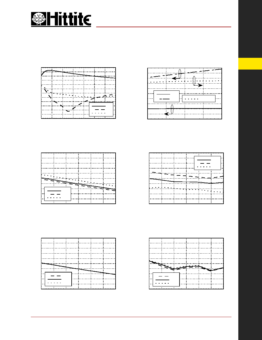
LNA Broadband Gain & Return Loss
LNA Gain vs. Temperature
LNA Noise Figure vs. Temperature
-40
-35
-30
-25
-20
-15
-10
-5
0
5
10
15
20
0.25
0.5
0.75
1
1.25
1.5
1.75
2
S21
S11
S22
RESPONSE (dB)
FREQUENCY (GHz)
10
11
12
13
14
15
16
17
18
19
20
0.7
0.75
0.8
0.85
0.9
0.95
1
+25 C
+85 C
-40 C
GAIN
(dB)
FREQUENCY (GHz)
0.5
0.6
0.7
0.8
0.9
1
1.1
1.2
1.3
1.4
1.5
0.7
0.75
0.8
0.85
0.9
0.95
1
+25 C
+85 C
-40 C
NOI
SE FI
GURE (dB)
FREQUENCY (GHz)
LNA ≠ Gain, Noise Figure &
Power vs. Supply Voltage @ 850 MHz
12
13
14
15
16
17
18
19
20
21
22
0.2
0.3
0.4
0.5
0.6
0.7
0.8
0.9
1
1.1
1.2
4.5
4.75
5
5.25
5.5
Gain
P1dB
Noise Figure
GAIN (dB), P1dB (dBm)
NOI
SE FI
GURE (dB)
Vdd (Vdc)
LNA Gain vs. Vdd
LNA Noise Figure vs. Vdd
10
11
12
13
14
15
16
17
18
19
20
0.7
0.75
0.8
0.85
0.9
0.95
1
+4.5 V
+5.0 V
+5.5 V
GAIN
(dB)
FREQUENCY (GHz)
0.5
0.6
0.7
0.8
0.9
1
1.1
1.2
1.3
1.4
1.5
0.7
0.75
0.8
0.85
0.9
0.95
1
+4.5 V
+5.0 V
+5.5 V
NOI
SE FI
GURE (dB)
FREQUENCY (GHz)
MICROWAVE CORPORATION
8 - 134
For price, delivery, and to place orders, please contact Hittite Microwave Corporation:
12 Elizabeth Drive, Chelmsford, MA 01824 Phone: 978-250-3343 Fax: 978-250-3373
Order Online at www.hittite.com
AMPLIFIERS - SMT
8
HMC373LP3
v01.0604
GaAs PHEMT MMIC LOW NOISE
AMPLIFIER w/ BYPASS MODE, 700 - 1000 MHz
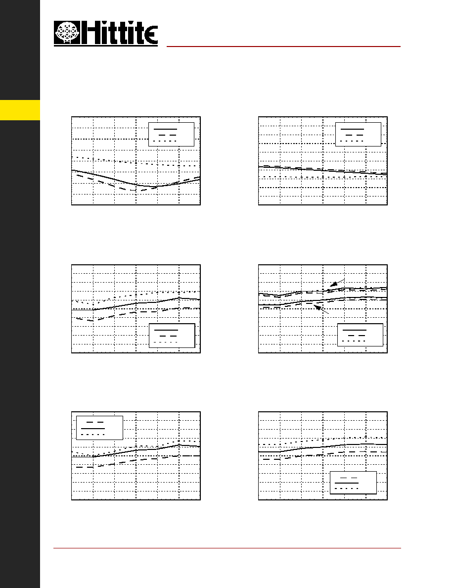
LNA Output IP3 vs. Temperature
LNA P1dB & Psat vs. Temperature
LNA Output IP3 vs. Vdd
LNA P1dB vs. Vdd
LNA Input Return Loss vs. Temperature
LNA Output Return Loss vs. Temperature
-40
-35
-30
-25
-20
-15
-10
-5
0
0.7
0.75
0.8
0.85
0.9
0.95
1
+25 C
+85 C
-40 C
RETURN LOSS (dB)
FREQUENCY (GHz)
-20
-18
-16
-14
-12
-10
-8
-6
-4
-2
0
0.7
0.75
0.8
0.85
0.9
0.95
1
+25 C
+85 C
-40 C
RETURN LOSS (dB)
FREQUENCY (GHz)
30
31
32
33
34
35
36
37
38
39
40
0.7
0.75
0.8
0.85
0.9
0.95
1
+25 C
+85 C
-40 C
OUTPUT IP3 (dBm)
FREQUENCY (GHz)
30
31
32
33
34
35
36
37
38
39
40
0.7
0.75
0.8
0.85
0.9
0.95
1
+4.5 V
+5.0 V
+5.5 V
OUTPUT IP3 (dBm)
FREQUENCY (GHz)
15
16
17
18
19
20
21
22
23
24
25
0.7
0.75
0.8
0.85
0.9
0.95
1
+25 C
+85 C
-40 C
COMPRESSION POINT (dBm)
FREQUENCY (GHz)
P1dB
Psat
15
16
17
18
19
20
21
22
23
24
25
0.7
0.75
0.8
0.85
0.9
0.95
1
+4.5 V
+5.0 V
+5.5 V
P1dB (dBm)
FREQUENCY (GHz)

MICROWAVE CORPORATION
8 - 135
For price, delivery, and to place orders, please contact Hittite Microwave Corporation:
12 Elizabeth Drive, Chelmsford, MA 01824 Phone: 978-250-3343 Fax: 978-250-3373
Order Online at www.hittite.com
AMPLIFIERS - SMT
8
HMC373LP3
v01.0604
GaAs PHEMT MMIC LOW NOISE
AMPLIFIER w/ BYPASS MODE, 700 - 1000 MHz
Bypass Mode
Insertion Loss vs. Temperature
Bypass Mode
Input Return Loss vs. Temperature
Bypass Mode
Output Return Loss vs. Temperature
Bypass Mode
Input IP3 vs. Temperature
Bypass Mode
Broadband Insertion Loss & Return Loss
LNA Reverse Isolation vs. Temperature
-30
-25
-20
-15
-10
-5
0
0.7
0.75
0.8
0.85
0.9
0.95
1
+25 C
+85 C
-40 C
ISOLATION (dB)
FREQUENCY (GHz)
-40
-35
-30
-25
-20
-15
-10
-5
0
0.25
0.5
0.75
1
1.25
1.5
1.75
2
S21
S11
S22
RESPONSE (dB)
FREQUENCY (GHz)
-5
-4.5
-4
-3.5
-3
-2.5
-2
-1.5
-1
-0.5
0
0.7
0.75
0.8
0.85
0.9
0.95
1
+25 C
+85 C
-40 C
INSERTION LOSS (dB)
FREQUENCY (GHz)
-40
-35
-30
-25
-20
-15
-10
-5
0
0.7
0.75
0.8
0.85
0.9
0.95
1
+25 C
+85 C
-40 C
RETURN LOSS (dB)
FREQUENCY (GHz)
-50
-45
-40
-35
-30
-25
-20
-15
-10
-5
0
0.7
0.75
0.8
0.85
0.9
0.95
1
+25 C
+85 C
-40 C
RETURN LOSS (dB)
FREQUENCY (GHz)
35
40
45
50
55
0.7
0.75
0.8
0.85
0.9
0.95
1
+25 C
+85 C
-40 C
INPUT IP3 (dBm)
FREQUENCY (GHz)

MICROWAVE CORPORATION
8 - 136
For price, delivery, and to place orders, please contact Hittite Microwave Corporation:
12 Elizabeth Drive, Chelmsford, MA 01824 Phone: 978-250-3343 Fax: 978-250-3373
Order Online at www.hittite.com
AMPLIFIERS - SMT
8
HMC373LP3
v01.0604
GaAs PHEMT MMIC LOW NOISE
AMPLIFIER w/ BYPASS MODE, 700 - 1000 MHz
Typical Supply Current vs. Vdd
Vdd (Vdc)
Idd (mA)
+4.5
87
+5.0
90
+5.5
93
Drain Bias Voltage (Vdd)
+8.0 Vdc
RF Input Power
(RFin)(Vdd = +5.0 Vdc)
LNA Mode
Bypass Mode
+15 dBm
+30 dBm
Channel Temperature
150 ∞C
Continuous Pdiss (T = 85 ∞C)
(derate 13.5 mW/∞C above 85 ∞C)
0.878 W
Thermal Resistance
(channel to ground paddle)
74.1 ∞C/W
Storage Temperature
-65 to +150∞ C
Operating Temperature
-40 to +85∞ C
Absolute Maximum Ratings
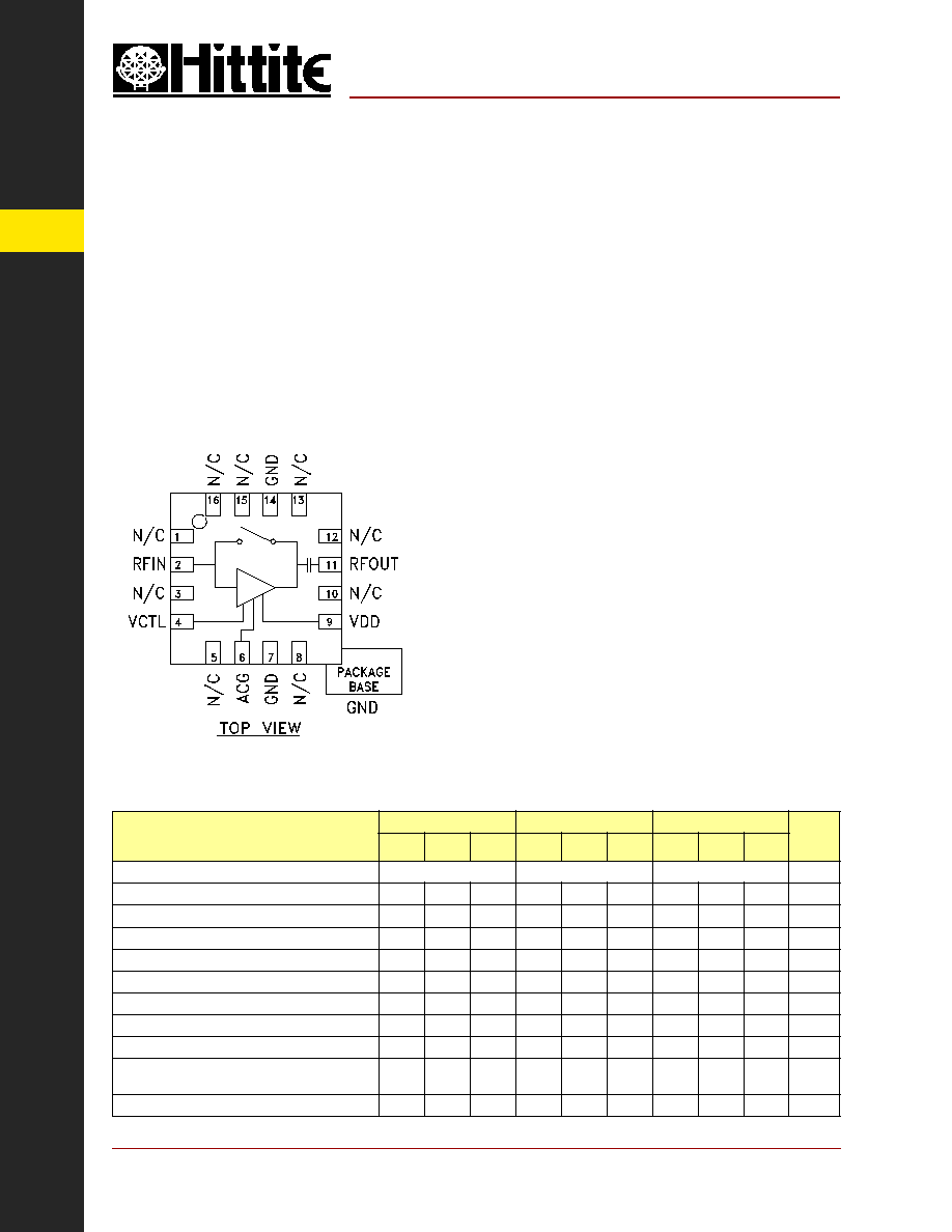
Outline Drawing
NOTES:
1. MATERIAL PACKAGE BODY: LOW STRESS INJECTION MOLDED
PLASTIC SILICA AND SILICON IMPREGNATED.
2. LEAD AND GROUND PADDLE MATERIAL: COPPER ALLOY
3. LEAD AND GROUND PADDLE PLATING: Sn/Pb SOLDER
4. DIMENSIONS ARE IN INCHES [MILLIMETERS].
5. LEAD SPACING TOLERANCE IS NON-CUMULATIVE
6. PAD BURR LENGTH SHALL BE 0.15mm MAXIMUM.
PAD BURR HEIGHT SHALL BE 0.05mm MAXIMUM.
7. PACKAGE WARP SHALL NOT EXCEED 0.05mm.
8. ALL GROUND LEADS AND GROUND PADDLE MUST BE SOLDERED
TO PCB RF GROUND.
9. REFER TO HITTITE APPLICATION NOTE FOR SUGGESTED PCB
LAND
PATTERN.
LNA Mode
Vctl= Short Circuit to DC Ground
Bypass Mode
Vctl= Open Circuit
Truth Table

MICROWAVE CORPORATION
8 - 137
For price, delivery, and to place orders, please contact Hittite Microwave Corporation:
12 Elizabeth Drive, Chelmsford, MA 01824 Phone: 978-250-3343 Fax: 978-250-3373
Order Online at www.hittite.com
AMPLIFIERS - SMT
8
HMC373LP3
v01.0604
GaAs PHEMT MMIC LOW NOISE
AMPLIFIER w/ BYPASS MODE, 700 - 1000 MHz
Pin Descriptions
Pin Number
Function
Description
Interface Schematic
1, 3, 5, 8, 10,
12, 13, 15, 16
N/C
No connection necessary.
These pins may be connected to RF/DC ground.
2
RF IN
This pin is matched to 50 Ohms with a 19 nH inductor to
ground. See Application Circuit.
4
Vctl
DC ground return. LNA is in high gain mode when a short
circuit is introduced to this pin through an external switch.
LNA is in bypass mode when open circuit is introduced
6
ACG
An external capacitor of 0.01µF to ground is required
for low frequency bypassing.
See Application Circuit for further details.
7, 14
GND
These pins must be connected to RF/DC ground.
9
Vdd
Power supply voltage. Choke inductor and bypass capacitor
are required. See application circuit.
11
RF OUT
This pin is AC coupled and matched to 50 Ohms.
MICROWAVE CORPORATION
8 - 138
For price, delivery, and to place orders, please contact Hittite Microwave Corporation:
12 Elizabeth Drive, Chelmsford, MA 01824 Phone: 978-250-3343 Fax: 978-250-3373
Order Online at www.hittite.com
AMPLIFIERS - SMT
8
HMC373LP3
v01.0604
GaAs PHEMT MMIC LOW NOISE
AMPLIFIER w/ BYPASS MODE, 700 - 1000 MHz
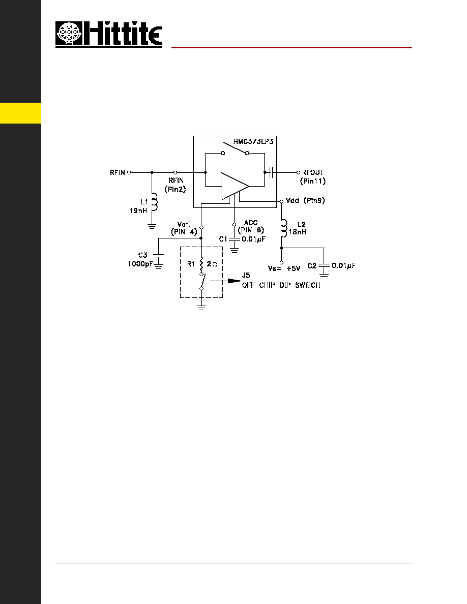
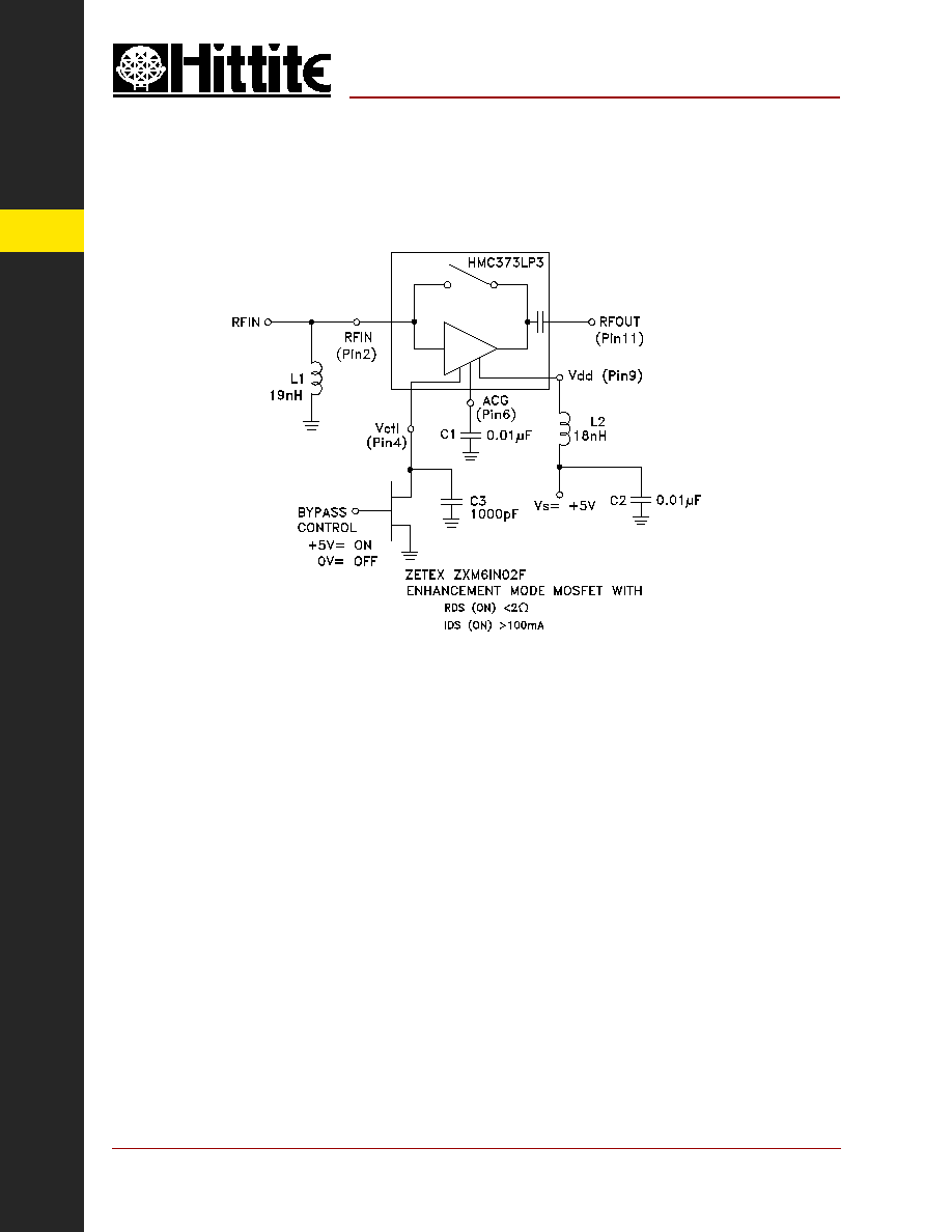
Note 1: Choose value of capacitor C1 for low frequency bypassing. A 0.01 µF ±10% capacitor is recommended.
Note 2: Pin 4 (Vctl) is the DC ground return for the circuit. The LNA is in the high gain mode when a short circuit is introduced to this
pin through an external switch. The LNA is in bypass mode when an open circuit is introduced. For the data presented, switching is
done through a two position DIP switch (J5) in series with a 2 Ohm resistor (to account for the Ron of an electrical switch).
Note 3: L1, L2 and C1 should be located as close to pins as possible.
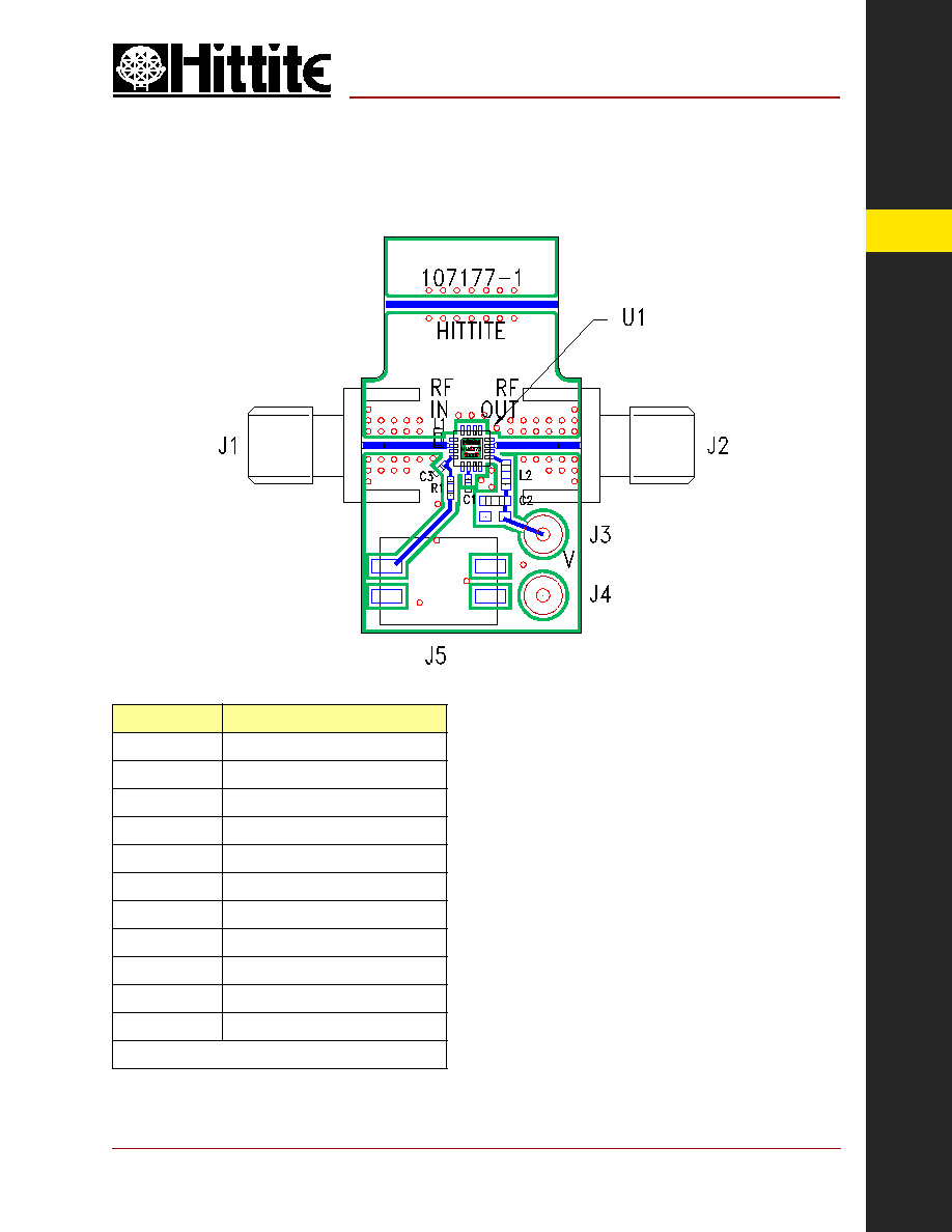
Evaluation Board Circuit
MICROWAVE CORPORATION
8 - 139
For price, delivery, and to place orders, please contact Hittite Microwave Corporation:
12 Elizabeth Drive, Chelmsford, MA 01824 Phone: 978-250-3343 Fax: 978-250-3373
Order Online at www.hittite.com
AMPLIFIERS - SMT
8
HMC373LP3
v01.0604
GaAs PHEMT MMIC LOW NOISE
AMPLIFIER w/ BYPASS MODE, 700 - 1000 MHz
Item
Description
J1 - J2
PC Mount SMA RF Connector
J3 - J4
DC Pin
J5
2 Pos DIP Switch
C1
10000 pF Capacitor, 0402 Pkg.
C2
10000 pF Capacitor, 0603 Pkg.
C3
1000 pF Capacitor, 0402 Pkg.
L1
19 nH Inductor, 0402 Pkg.
L2
18 nH Inductor, 0603 Pkg.
R1
2 Ohm Resistor, 0402 Pkg.
U1
HMC373LP3 Amplifi er
PCB*
107177 Evaluation Board
* Circuit Board Material: Rogers 4350
Evaluation PCB
The circuit board used in the fi nal application should
use RF circuit design techniques. Signal lines should
have 50 ohm impedance while the package ground
leads and exposed paddle should be connected directly
to the ground plane similar to that shown. A suffi cient
number of VIA holes should be used to connect the top
and bottom ground planes. The evaluation circuit board
shown is available from Hittite upon request.
List of Material
MICROWAVE CORPORATION
8 - 140
For price, delivery, and to place orders, please contact Hittite Microwave Corporation:
12 Elizabeth Drive, Chelmsford, MA 01824 Phone: 978-250-3343 Fax: 978-250-3373
Order Online at www.hittite.com
AMPLIFIERS - SMT
8
HMC373LP3
v01.0604
GaAs PHEMT MMIC LOW NOISE
AMPLIFIER w/ BYPASS MODE, 700 - 1000 MHz
Application Circuit
Note 1: Choose value of capacitor C1 for low frequency bypassing. A 0.01 µF ±10% capacitor is recommended.
Note 2: Pin 4 (Vctl) is the DC ground return for the circuit. The LNA is in the high gain mode when a short circuit is introduced to this
pin through an external switch. The LNA is in bypass mode when an open circuit is introduced. For the data presented, switching is
done through a two position DIP switch (J5) in series with a 2 Ohm resistor (to account for the Ron of an electrical switch).
Note 3: L1, L2 and C1 should be located as close to pins as possible.

MICROWAVE CORPORATION
8 - 141
For price, delivery, and to place orders, please contact Hittite Microwave Corporation:
12 Elizabeth Drive, Chelmsford, MA 01824 Phone: 978-250-3343 Fax: 978-250-3373
Order Online at www.hittite.com
AMPLIFIERS - SMT
8
HMC373LP3
v01.0604
GaAs PHEMT MMIC LOW NOISE
AMPLIFIER w/ BYPASS MODE, 700 - 1000 MHz
Notes: