 | –≠–ª–µ–∫—Ç—Ä–æ–Ω–Ω—ã–π –∫–æ–º–ø–æ–Ω–µ–Ω—Ç: HMC424 | –°–∫–∞—á–∞—Ç—å:  PDF PDF  ZIP ZIP |

MICROWAVE CORPORATION
2 - 8
For price, delivery, and to place orders, please contact Hittite Microwave Corporation:
12 Elizabeth Drive, Chelmsford, MA 01824 Phone: 978-250-3343 Fax: 978-250-3373
Order Online at www.hittite.com
A
TTENU
A
T
ORS - CHIP
2
HMC424
0.5dB LSB GaAs MMIC 6-BIT DIGITAL
ATTENUATOR, DC - 13 GHz
v02.0404
Functional Diagram
Electrical Specifi cations,
T
A
= +25∞ C, With Vee = -5V & VCTL = 0/-5V
Typical Applications
The HMC424 is ideal for:
∑ Fiber Optics & Broadband Telecom
∑ Microwave Radio & VSAT
∑ Military Radios, Radar, & ECM
∑ Space Applications
Features
0.5 dB LSB Steps to 31.5 dB
Single Control Line Per Bit
+/- 0.5 dB Typical Bit Error
Die Size: 0.85 mm x 1.45 mm x 0.1 mm
General Description
The HMC424 die is a broadband 6-bit GaAs IC
digital attenuator MMIC chip. Covering DC to 13
GHz, the insertion loss is less then 4 dB typical.
The attenuator bit values are 0.5 (LSB), 1, 2, 4,
8, and 16 dB for a total attenuation of 31.5 dB.
Attenuation accuracy is excellent at ± 0.5 dB typi-
cal step error with an IIP3 of +32 dBm. Six con-
trol voltage inputs, toggled between 0 and -5V,
are used to select each attenuation state. A single
Vee bias of -5V allows operation at frequencies
down to DC.
Parameter
Frequency (GHz)
Min.
Typ.
Max.
Units
Insertion Loss
DC - 8.0 GHz
8.0 - 13.0 GHz
3.0
4.0
3.8
4.6
dB
dB
Attenuation Range
DC - 13.0 GHz
31.5
dB
Return Loss (RF1 & RF2, All Atten. States)
DC - 8.0 GHz
8.0 - 13.0 GHz
8
11
12
15
dB
dB
Attenuation Accuracy: (Referenced to Insertion Loss)
0.5 - 7.5 dB States
8 - 31.5 dB States
DC - 13.0 GHz
DC - 13.0 GHz
± 0.3 + 4% of Atten. Setting Max
± 0.3 + 6% of Atten. Setting Max
dB
dB
Input Power for 0.1 dB Compression
1.0 - 13.0 Ghz
22
dBm
Input Third Order Intercept Point
(Two-Tone Input Power= 0 dBm Each Tone)
REF State
All Other States
1.0 - 13.0 Ghz
46
32
dBm
dBm
Switching Characteristics
tRISE, tFALL (10/90% RF)
tON/tOFF (50% CTL to 10/90% RF)
DC - 13.0 GHz
30
50
ns
ns

MICROWAVE CORPORATION
2 - 9
For price, delivery, and to place orders, please contact Hittite Microwave Corporation:
12 Elizabeth Drive, Chelmsford, MA 01824 Phone: 978-250-3343 Fax: 978-250-3373
Order Online at www.hittite.com
A
TTENU
A
T
ORS - CHIP
2
-10
-9
-8
-7
-6
-5
-4
-3
-2
-1
0
0
1
2
3
4
5
6
7
8
9
10 11 12 13 14 15
+25 C
+85 C
-55 C
INSERTION LOSS (dB)
FREQUENCY (GHz)
-25
-20
-15
-10
-5
0
0
1
2
3
4
5
6
7
8
9
10 11 12 13 14 15
0.5 dB
1 dB
2 dB
4 dB
8 dB
16 dB
31.5 dB
RETURN LOSS (dB)
FREQUENCY (GHz)
-35
-30
-25
-20
-15
-10
-5
0
0
1
2
3
4
5
6
7
8
9
10 11 12 13 14 15
0.5 dB
1 dB
2 dB
4 dB
8 dB
16 dB
31.5 dB
NORMALIZED ATTENUATION (dB)
FREQUENCY (GHz)
-2
-1.5
-1
-0.5
0
0.5
1
1.5
2
0
4
8
12
16
20
24
28
32
0.1 GHz
4 GHz
8 GHz
13 GHz
BIT ERROR (dB)
ATTENUATION STATE (dB)
-2
-1.5
-1
-0.5
0
0.5
1
1.5
2
0
1
2
3
4
5
6
7
8
9
10 11 12 13 14 15
0.5 dB
1 dB
2 dB
4 dB
8 dB
16 dB
31.5 dB
BIT ERROR (dB)
FREQUENCY (GHz)
-20
0
20
40
60
80
100
0
1
2
3
4
5
6
7
8
9
10 11 12 13 14 15
0.5 dB
1 dB
2 dB
4 dB
8 dB
16 dB
31.5 dB
RELATIVE PHASE (deg)
FREQUENCY (GHz)
GaAs MMIC SUB-HARMONICALLY PUMPED MIXER 17 - 25 GHz
HMC424
Return Loss RF1, RF2
(Only Major States are Shown)
0.5dB LSB GaAs MMIC 6-BIT DIGITAL
ATTENUATOR, DC - 13 GHz
v02.0404
Insertion Loss
Normalized Attenuation
(Only Major States are Shown)
Bit Error vs. Frequency
(Only Major States are Shown)
Relative Phase vs. Frequency
(Only Major States are Shown)
Bit Error vs. Attenuation State

MICROWAVE CORPORATION
2 - 10
For price, delivery, and to place orders, please contact Hittite Microwave Corporation:
12 Elizabeth Drive, Chelmsford, MA 01824 Phone: 978-250-3343 Fax: 978-250-3373
Order Online at www.hittite.com
A
TTENU
A
T
ORS - CHIP
2
HMC424
0.5dB LSB GaAs MMIC 6-BIT DIGITAL
ATTENUATOR, DC - 13 GHz
v02.0404
Truth Table
Control Voltage
Bias Voltage & Current
-2
-1.5
-1
-0.5
0
0.5
1
1.5
2
0
1
2
3
4
5
6
7
8
9
10 11 12 13 14 15
STEP ERROR (dB)
FREQUENCY (GHz)
Worst Case Step Error
Between Successive Attenuation States
Absolute Maximum Ratings
Control Voltage Input
Attenuation
State
RF1 - RF2
V1
16 dB
V2
8 dB
V3
4 dB
V4
2 dB
V5
1 dB
V6
0.5 dB
Low
Low
Low
Low
Low
Low
Reference
I.L.
Low
Low
Low
Low
Low
High
0.5 dB
Low
Low
Low
Low
High
Low
1 dB
Low
Low
Low
High
Low
Low
2 dB
Low
Low
High
Low
Low
Low
4 dB
Low
High
Low
Low
Low
Low
8 dB
High
Low
Low
Low
Low
Low
16 dB
High
High
High
High
High
High
31.5 dB
Any Combination of the above states will provide
an attenuation approximately equal to the sum of
the bits selected.
State
Bias Condition
Low
0 to -3V @ 70 µA Typ.
High
-5 to -4.2V @ 5 µA Typ.
Vee Range= -5.0 Vdc ± 10%
Vee
(Vdc)
Iee (Typ.)
(mA)
Iee (Max.)
(mA)
-5.0
2
4
Control Voltage (V1 to V6)
Vee - 0.5 Vdc
Bias Voltage (Vee)
-7.0 Vdc
Channel Temperature
150 ∞C
Thermal Resistance
140 ∞C/W
Storage Temperature
-65 to + 150 ∞C
Operating Temperature
-55 to +85 ∞C
RF Input Power (0.5 - 13.0 GHz)
+25 dBm

MICROWAVE CORPORATION
2 - 11
For price, delivery, and to place orders, please contact Hittite Microwave Corporation:
12 Elizabeth Drive, Chelmsford, MA 01824 Phone: 978-250-3343 Fax: 978-250-3373
Order Online at www.hittite.com
A
TTENU
A
T
ORS - CHIP
2
Outline Drawing
1. ALL DIMENSIONS ARE IN INCHES (MILLIMETERS).
2. TYPICAL BOND PAD IS .004" SQUARE.
3. TYPICAL BOND PAD SPACING IS .006" CENTER TO CENTER EXCEPT AS NOTED.
4. BACKSIDE METALIZATION: GOLD
5. BACKSIDE METAL IS GROUND
6. BOND PAD METALIZATION: GOLD
HMC424
0.5dB LSB GaAs MMIC 6-BIT DIGITAL
ATTENUATOR, DC - 13 GHz
v02.0404
Pad Number
Function
Description
Interface Schematic
GND
Die bottom must be connected to RF ground.
1, 3
RF1, RF2
This pad is DC coupled and matched to 50 Ohm. Blocking capaci-
tors are required if RF line potential is not equal to 0V.
2
VEE
Supply Voltage -5V
±
10%
4, 5, 6, 7, 8, 9
V1 - V6
See truth table and control voltage table.
Pad Descriptions
MICROWAVE CORPORATION
2 - 12
For price, delivery, and to place orders, please contact Hittite Microwave Corporation:
12 Elizabeth Drive, Chelmsford, MA 01824 Phone: 978-250-3343 Fax: 978-250-3373
Order Online at www.hittite.com
A
TTENU
A
T
ORS - CHIP
2
HMC424
0.5dB LSB GaAs MMIC 6-BIT DIGITAL
ATTENUATOR, DC - 13 GHz
v02.0404
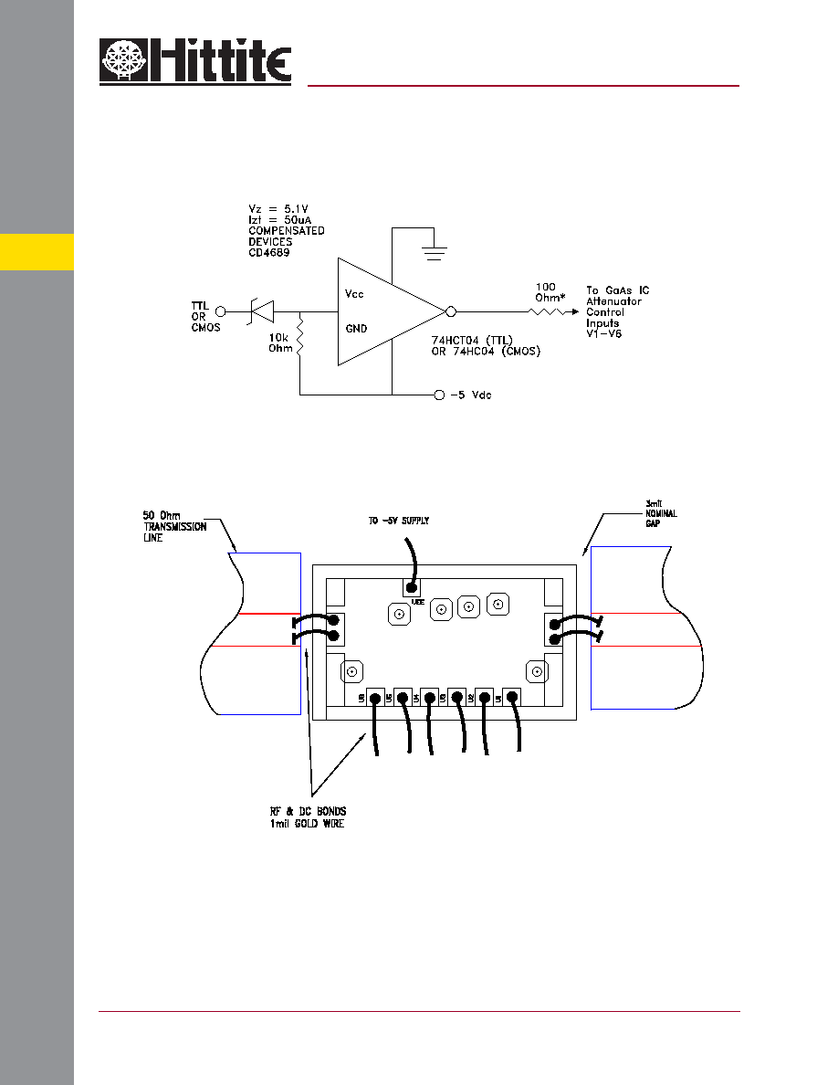
Suggested Driver Circuit
(One Circuit Required Per Bit Control Input)
Simple driver using inexpensive standard logic ICs provides fast switching using minimum DC current.
* Recommended value to suppress unwanted RF signals at V1 - V6 control lines.
Mounting & Bonding Techniques for Millimeterwave GaAs MMICs
The die should be attached directly to the ground plane eutectically or with conductive epoxy (see HMC general Handling,
Mounting, Bonding Note).
50 Ohm Microstrip transmission lines on 0.127mm (5 mil) thick alumina thin fi lm substrates are recommended for bringing RF
to and from the chip (Figure 1). If 0.254mm (10 mil) thick alumina thin fi lm substrates must be used, the die should be raised
0.150mm (6 mils) so that the surface of the die is coplanar with the surface of the substrate. One way to accomplish this is to
attach the 0.102mm (4 mil) thick die to a 0.150mm (6 mil) thick molybdenum heat spreader (moly-tab) which is then attached
to the ground plane (Figure 2).
Microstrip substrates should be brought as close to the die as possible in order to minimize bond wire length. Typical die-to-
substrate spacing is 0.076mm to 0.152 mm (3 to 6 mils).
Assembly Diagram