 | –≠–ª–µ–∫—Ç—Ä–æ–Ω–Ω—ã–π –∫–æ–º–ø–æ–Ω–µ–Ω—Ç: HMC425 | –°–∫–∞—á–∞—Ç—å:  PDF PDF  ZIP ZIP |
MICROWAVE CORPORATION
2 - 14
For price, delivery, and to place orders, please contact Hittite Microwave Corporation:
12 Elizabeth Drive, Chelmsford, MA 01824 Phone: 978-250-3343 Fax: 978-250-3373
Order Online at www.hittite.com
A
TTENU
A
T
ORS - CHIP
2
HMC425
0.5 dB LSB GaAs MMIC 6-BIT DIGITAL
POSITIVE CONTROL ATTENUATOR, 2.4 - 8.0 GHz
v01.0402
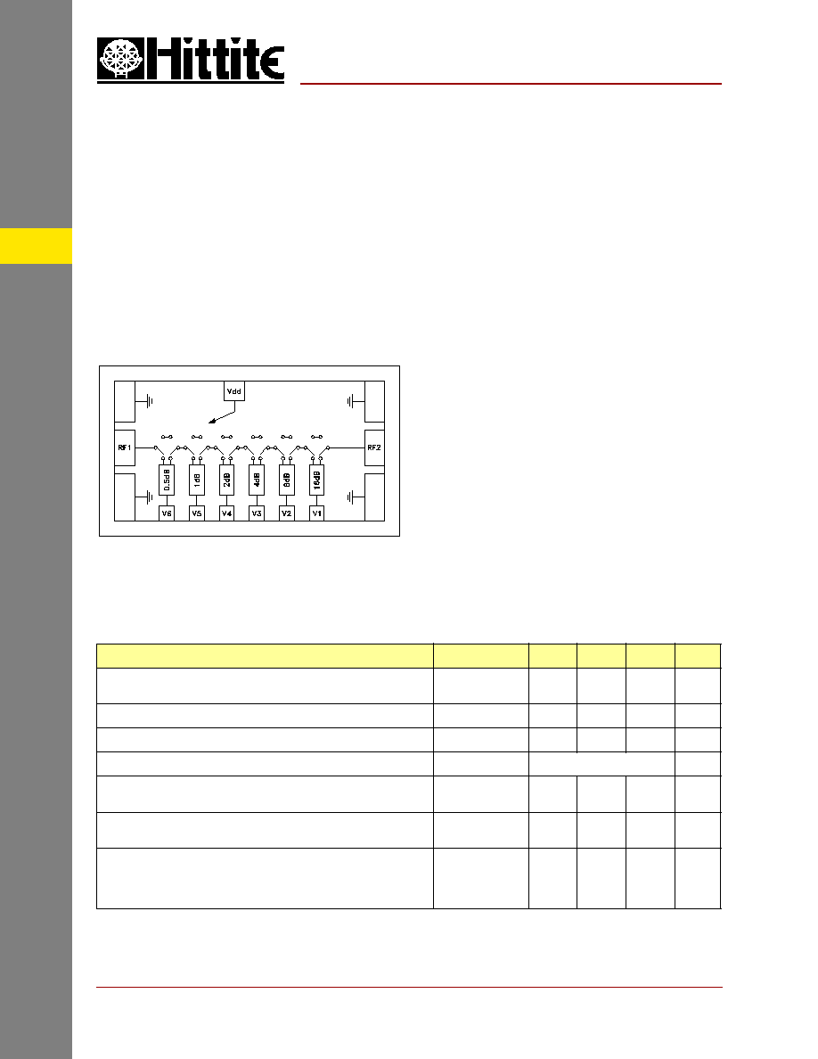
Functional Diagram
Electrical Specifi cations,
T
A
= +25∞ C, With Vdd = +5V & Vctl = 0/+5V (Unless Otherwise Noted)
Typical Applications
The HMC425 is ideal for:
∑ Fiber Optics & Broadband Telecom
∑ Microwave Radio & VSAT
∑ Military Radios, Radar, & ECM
∑ Space Applications
Features
0.5 dB LSB Steps to 31.5 dB
Single Control Line Per Bit
+/- 0.5 dB Typical Bit Error
Die Size: 0.85 mm x 1.5 mm x 0.1 mm
General Description
The HMC425 die is a broadband 6-bit GaAs IC
digital attenuator MMIC chip. Covering 2.4 to 8.0
GHz, the insertion loss is less then 3.5 dB typical.
The attenuator bit values are 0.5 (LSB), 1, 2, 4,
8, and 16 dB for a total attenuation of 31.5 dB.
Attenuation accuracy is excellent at ± 0.5 dB typi-
cal step error with an IIP3 of +40 dBm. Six con-
trol voltage inputs, toggled between 0 and +3 to
+5V, are used to select each attenuation state. A
single Vdd bias of +3 to +5V is required.
Parameter
Frequency (GHz)
Min.
Typ.
Max.
Units
Insertion Loss
2.4 - 6.0 GHz
6.0 - 8.0 GHz
2.7
3.5
3.2
4.0
dB
dB
Attenuation Range
2.4 - 8.0 GHz
31.5
dB
Return Loss (RF1 & RF2, All Atten. States)
2.4 - 8.0 GHz
12
15
dB
Attenuation Accuracy: (Referenced to Insertion Loss)
All States
2.4 - 8.0 GHz
± 0.4 + 4% of Atten. Setting Max
dB
Input Power for 0.1 dB Compression
Vdd= 5V
Vdd= 3V
2.4 - 8.0 GHz
22
19
dBm
dBm
Input Third Order Intercept Point
(Two-Tone Input Power= 0 dBm Each Tone)
REF - 16.0 dB States
16.5 - 31.5 dB States
2.4 - 8.0 GHz
45
35
dBm
dBm
Switching Characteristics
tRISE, tFALL (10/90% RF)
tON/tOFF (50% CTL to 10/90% RF)
2.4 - 8.0 GHz
160
180
ns
ns

MICROWAVE CORPORATION
2 - 15
For price, delivery, and to place orders, please contact Hittite Microwave Corporation:
12 Elizabeth Drive, Chelmsford, MA 01824 Phone: 978-250-3343 Fax: 978-250-3373
Order Online at www.hittite.com
A
TTENU
A
T
ORS - CHIP
2
-10
-9
-8
-7
-6
-5
-4
-3
-2
-1
0
1
2
3
4
5
6
7
8
9
10
+25 C
+85 C
-55 C
INSERTION LOSS (dB)
FREQUENCY (GHz)
-25
-20
-15
-10
-5
0
1
2
3
4
5
6
7
8
9
10
0.5 dB
1 dB
2 dB
4 dB
8 dB
16 dB
31.5 dB
RETURN LOSS (dB)
FREQUENCY (GHz)
-35
-30
-25
-20
-15
-10
-5
0
1
2
3
4
5
6
7
8
9
10
0.5 dB
1 dB
2 dB
4 dB
8 dB
16 dB
31.5 dB
NORMALIZED ATTENUATION (dB)
FREQUENCY (GHz)
-2
-1.5
-1
-0.5
0
0.5
1
1.5
2
0
2
4
6
8 10 12 14 16 18 20 22 24 26 28 30 32
2.4 GHz
3.5 GHz
5.5 GHz
8.0 GHz
BIT ERROR (dB)
ATTENUATION STATE (dB)
-2
-1.5
-1
-0.5
0
0.5
1
1.5
2
1
2
3
4
5
6
7
8
9
10
0.5 dB
1 dB
2 dB
4 dB
8 dB
16 dB
31.5 dB
BIT ERROR (dB)
FREQUENCY (GHz)
-40
-20
0
20
40
60
80
1
2
3
4
5
6
7
8
9
10
0.5 dB
1 dB
2 dB
4 dB
8 dB
16 dB
31.5 dB
RELATIVE PHASE (deg)
FREQUENCY (GHz)
GaAs MMIC SUB-HARMONICALLY PUMPED MIXER 17 - 25 GHz
HMC425
Return Loss RF1, RF2
(Only Major States are Shown)
v01.0402
Insertion Loss
Normalized Attenuation
(Only Major States are Shown)
Bit Error vs. Frequency
(Only Major States are Shown)
Relative Phase vs. Frequency
(Only Major States are Shown)
Bit Error vs. Attenuation State
0.5 dB LSB GaAs MMIC 6-BIT DIGITAL
POSITIVE CONTROL ATTENUATOR, 2.4 - 8.0 GHz

MICROWAVE CORPORATION
2 - 16
For price, delivery, and to place orders, please contact Hittite Microwave Corporation:
12 Elizabeth Drive, Chelmsford, MA 01824 Phone: 978-250-3343 Fax: 978-250-3373
Order Online at www.hittite.com
A
TTENU
A
T
ORS - CHIP
2
HMC425
v01.0402
Truth Table
Control Voltage
Bias Voltage & Current
-2
-1.5
-1
-0.5
0
0.5
1
1.5
2
1
2
3
4
5
6
7
8
9
10
STEP ERROR (dB)
FREQUENCY (GHz)
0.5 dB LSB GaAs MMIC 6-BIT DIGITAL
POSITIVE CONTROL ATTENUATOR, 2.4 - 8.0 GHz
Worst Case Step Error
Between Successive Attenuation States
Absolute Maximum Ratings
Control Voltage Input
Attenuation
State
RF1 - RF2
V1
16 dB
V2
8 dB
V3
4 dB
V4
2 dB
V5
1 dB
V6
0.5 dB
High
High
High
High
High
High
Reference
I.L.
High
High
High
High
High
Low
0.5 dB
High
High
High
High
Low
High
1 dB
High
High
High
Low
High
High
2 dB
High
High
Low
High
High
High
4 dB
High
Low
High
High
High
High
8 dB
Low
High
High
High
High
High
16 dB
Low
Low
Low
Low
Low
Low
31.5 dB
Any Combination of the above states will provide
an attenuation approximately equal to the sum of
the bits selected.
State
Bias Condition
Low
0 to 0.2V @ 10 µA Typ.
High
Vdd ± 0.2V @ 5 µA Typ.
Note: Vdd= +3V to +5V
Vdd Range= +3.0 to +5.0 Vdc
Vdd
(Vdc)
Idd (Typ.)
(µA)
+3.0
10
+5.0
30
Control Voltage (V1 to V6)
Vdd +0.5 Vdc
Bias Voltage (Vdd)
+7.0 Vdc
Storage Temperature
-65 to + 150 ∞C
Operating Temperature
-55 to +85 ∞C
RF Input Power (2.4 - 8.0 GHz)
+30 dBm

MICROWAVE CORPORATION
2 - 17
For price, delivery, and to place orders, please contact Hittite Microwave Corporation:
12 Elizabeth Drive, Chelmsford, MA 01824 Phone: 978-250-3343 Fax: 978-250-3373
Order Online at www.hittite.com
A
TTENU
A
T
ORS - CHIP
2
Outline Drawing
HMC425
v01.0402
1. ALL DIMENSIONS ARE IN INCHES (MILLIMETERS).
2. TYPICAL BOND PAD IS .004" SQUARE.
3. TYPICAL BOND PAD SPACING IS .006" CENTER
TO CENTER EXCEPT AS NOTED.
4. BACKSIDE METALIZATION: GOLD
5. BACKSIDE METAL IS GROUND
6. BOND PAD METALIZATION: GOLD
0.5 dB LSB GaAs MMIC 6-BIT DIGITAL
POSITIVE CONTROL ATTENUATOR, 2.4 - 8.0 GHz
Pad Number
Function
Description
Interface Schematic
GND
Die bottom must be connected to RF ground.
1, 3
RF1, RF2
This pad is DC coupled and matched to 50 Ohm.
Blocking capacitors are required.
2
Vdd
Supply Voltage
4, 5, 6, 7, 8, 9
V1 - V6
See truth table and control voltage table.
Pad Descriptions

MICROWAVE CORPORATION
2 - 18
For price, delivery, and to place orders, please contact Hittite Microwave Corporation:
12 Elizabeth Drive, Chelmsford, MA 01824 Phone: 978-250-3343 Fax: 978-250-3373
Order Online at www.hittite.com
A
TTENU
A
T
ORS - CHIP
2
HMC425
v01.0402
0.5 dB LSB GaAs MMIC 6-BIT DIGITAL
POSITIVE CONTROL ATTENUATOR, 2.4 - 8.0 GHz
Mounting & Bonding Techniques for Millimeterwave GaAs MMICs
The die should be attached directly to the ground plane eutectically or with conductive epoxy (see HMC general Han-
dling, Mounting, Bonding Note).
50 Ohm Microstrip transmission lines on 0.127mm (5 mil) thick alumina thin fi lm substrates are recommended for
bringing RF to and from the chip (Figure 1). If 0.254mm (10 mil) thick alumina thin fi lm substrates must be used, the
die should be raised 0.150mm (6 mils) so that the surface of the die is coplanar with the surface of the substrate. One
way to accomplish this is to attach the 0.102mm (4 mil) thick die to a 0.150mm (6 mil) thick molybdenum heat spreader
(moly-tab) which is then attached to the ground plane (Figure 2).
Microstrip substrates should be brought as close to the die as possible in order to minimize bond wire length. Typical
die-to-substrate spacing is 0.076mm to 0.152 mm (3 to 6 mils).
Assembly Diagram

MICROWAVE CORPORATION
2 - 19
For price, delivery, and to place orders, please contact Hittite Microwave Corporation:
12 Elizabeth Drive, Chelmsford, MA 01824 Phone: 978-250-3343 Fax: 978-250-3373
Order Online at www.hittite.com
A
TTENU
A
T
ORS - CHIP
2
HMC425
v01.0402
0.5 dB LSB GaAs MMIC 6-BIT DIGITAL
POSITIVE CONTROL ATTENUATOR, 2.4 - 8.0 GHz
Handling Precautions
Follow these precautions to avoid permanent damage.
Cleanliness:
Handle the chips in a clean environment. DO NOT attempt to clean the chip using liquid cleaning systems.
Static Sensitivity:
Follow ESD precautions to protect against > ± 250V ESD strikes.
Transients:
Suppress instrument and bias supply transients while bias is applied. Use shielded signal and bias cables to minimize
inductive pick-up.
General Handling:
Handle the chip along the edges with a vacuum collet or with a sharp pair of bent tweezers. The surface of the chip has
fragile air bridges and should not be touched with vacuum collet, tweezers, or fi ngers.
Mounting
The chip is back-metallized and can be die mounted with AuSn eutectic preforms or with electrically conductive epoxy.
The mounting surface should be clean and fl at.
Eutectic Die Attach:
A 80/20 gold tin preform is recommended with a work surface temperature of 255 deg. C and a tool temperature of 265
deg. C. When hot 90/10 nitrogen/hydrogen gas is applied, tool tip temperature should be 290 deg. C. DO NOT expose
the chip to a temperature greater than 320 deg. C for more than 20 seconds. No more than 3 seconds of scrubbing
should be required for attachment.
Epoxy Die Attach:
Apply a minimum amount of epoxy to the mounting surface so that a thin epoxy fi llet is observed around the perimeter
of the chip once it is placed into position. Cure epoxy per the manufacturer's schedule.
Wire Bonding
Ball or wedge bond with 0.025 mm (1 mil) diameter pure gold wire. Thermosonic wirebonding with a nominal stage
temperature of 150 deg. C and a ball bonding force of 40 to 50 grams or wedge bonding force of 18 to 22 grams is rec-
ommended. Use the minimum level of ultrasonic energy to achieve reliable wirebonds. Wirebonds should be started on
the chip and terminated on the package or substrate. All bonds should be as short as possible <0.31 mm (12 mils).