 | ÐлекÑÑоннÑй компоненÑ: HMC425LP3 | СкаÑаÑÑ:  PDF PDF  ZIP ZIP |
Äîêóìåíòàöèÿ è îïèñàíèÿ www.docs.chipfind.ru
MICROWAVE CORPORATION
9 - 92
For price, delivery, and to place orders, please contact Hittite Microwave Corporation:
12 Elizabeth Drive, Chelmsford, MA 01824 Phone: 978-250-3343 Fax: 978-250-3373
Order Online at www.hittite.com
A
TTENU
A
T
ORS - SMT
9
HMC425LP3
0.5 dB LSB GaAs MMIC 6-BIT DIGITAL
POSITIVE CONTROL ATTENUATOR, 2.4 - 8.0 GHz
v00.0202
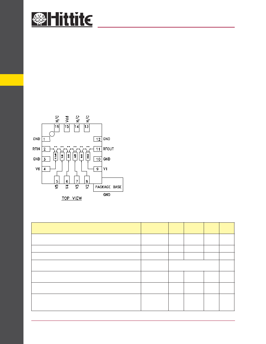
Functional Diagram
Electrical Specifi cations,
T
A
= +25° C, With Vdd = +5V & Vctl = 0/+5V (Unless Otherwise Noted)
Typical Applications
The HMC425LP3 is ideal for:
·
WLAN & Point-to-Multi-Point
·
Fiber Optics & Broadband Telecom
·
Microwave Radio & VSAT
·
Military
Features
0.5 dB LSB Steps to 31.5 dB
Single Control Line Per Bit
+/- 0.5 dB Typical Bit Error
Single +5V Supply
3 mm x 3 mm x 1 mm SMT Package
General Description
The HMC425LP3 is a broadband 6-bit GaAs IC
digital attenuator in a low cost leadless surface
mount package. Covering 2.4 to 8.0 GHz, the
insertion loss is less then 3.8 dB typical. The
attenuator bit values are 0.5 (LSB), 1, 2, 4, 8, and
16 dB for a total attenuation of 31.5 dB. Attenua-
tion accuracy is excellent at ± 0.5 dB typical step
error with an IIP3 of +40 dBm. Six control volt-
age inputs, toggled between 0 and +3 to +5V, are
used to select each attenuation state. A single
Vdd bias of +3 to +5V is required.
Parameter
Frequency
(GHz)
Min.
Typ.
Max.
Units
Insertion Loss
2.4 - 6.0 GHz
6.0 - 8.0 GHz
3.0
3.8
3.5
4.3
dB
dB
Attenuation Range
2.4 - 8.0 GHz
31.5
dB
Return Loss (RF1 & RF2, All Atten. States)
2.4 - 8.0 GHz
11
15
dB
Attenuation Accuracy:
(Referenced to Insertion Loss)
All States
2.4 - 8.0 GHz
± 0.5 + 5% of Atten. Setting Max.
dB
Input Power for 0.1 dB Compression
Vdd = 5V
Vdd = 3V
2.4 - 8.0 GHz
22
19
dBm
dBm
Input Third Order Intercept Point
(Two-Tone Input Power= 0 dBm Each Tone)
REF - 16.0 dB States
16.5 - 31.5 dB States
2.4 - 8.0 GHz
45
35
dBm
dBm
Switching Characteristics
tRISE, tFALL (10/90% RF)
tON, tOFF (50% CTL to 10/90% RF)
2.4 - 8.0 GHz
160
180
ns
ns
MICROWAVE CORPORATION
9 - 93
For price, delivery, and to place orders, please contact Hittite Microwave Corporation:
12 Elizabeth Drive, Chelmsford, MA 01824 Phone: 978-250-3343 Fax: 978-250-3373
Order Online at www.hittite.com
A
TTENU
A
T
ORS - SMT
9
-10
-9
-8
-7
-6
-5
-4
-3
-2
-1
0
1
2
3
4
5
6
7
8
9
10
+25 C
+85 C
-40 C
INSERTION LOSS (dB)
FREQUENCY (GHz)
-25
-20
-15
-10
-5
0
1
2
3
4
5
6
7
8
9
10
0.5 dB
1 dB
2 dB
4 dB
8 dB
16 dB
31.5 dB
RETURN LOSS (dB)
FREQUENCY (GHz)
-35
-30
-25
-20
-15
-10
-5
0
1
2
3
4
5
6
7
8
9
10
0.5 dB
1 dB
2 dB
4 dB
8 dB
16 dB
31.5 dB
NORMALIZED ATTENUATION (dB)
FREQUENCY (GHz)
-2
-1.5
-1
-0.5
0
0.5
1
1.5
2
0
2
4
6
8 10 12 14 16 18 20 22 24 26 28 30 32
2.4 GHz
3.5 GHz
5.5 GHz
8.0 GHz
BIT ERROR (dB)
ATTENUATION STATE (dB)
-2
-1.5
-1
-0.5
0
0.5
1
1.5
2
1
2
3
4
5
6
7
8
9
10
0.5 dB
1 dB
2 dB
4 dB
8 dB
16 dB
31.5 dB
BIT ERROR (dB)
FREQUENCY (GHz)
-40
-20
0
20
40
60
80
1
2
3
4
5
6
7
8
9
10
0.5 dB
1 dB
2 dB
4 dB
8 dB
16 dB
31.5 dB
RELATIVE PHASE (deg)
FREQUENCY (GHz)
GaAs MMIC SUB-HARMONICALLY PUMPED MIXER 17 - 25 GHz
HMC425LP3
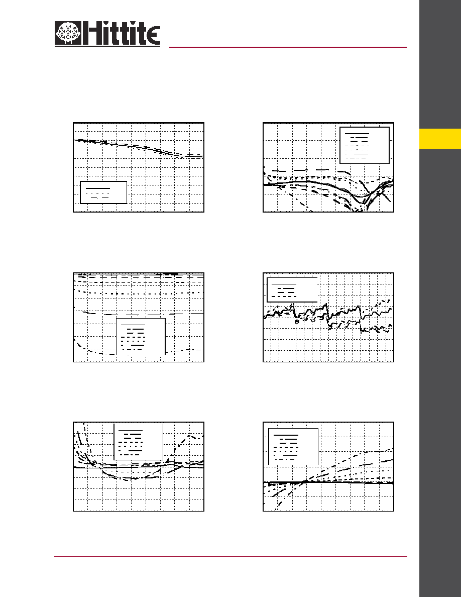
Return Loss RF1, RF2
(Only Major States are Shown)
v00.0202
Insertion Loss
Normalized Attenuation
(Only Major States are Shown)
Bit Error vs. Frequency
(Only Major States are Shown)
Relative Phase vs. Frequency
(Only Major States are Shown)
Bit Error vs. Attenuation State
0.5 dB LSB GaAs MMIC 6-BIT DIGITAL
POSITIVE CONTROL ATTENUATOR, 2.4 - 8.0 GHz
MICROWAVE CORPORATION
9 - 94
For price, delivery, and to place orders, please contact Hittite Microwave Corporation:
12 Elizabeth Drive, Chelmsford, MA 01824 Phone: 978-250-3343 Fax: 978-250-3373
Order Online at www.hittite.com
A
TTENU
A
T
ORS - SMT
9
HMC425LP3
v00.0202
Truth Table
Control Voltage
Bias Voltage & Current
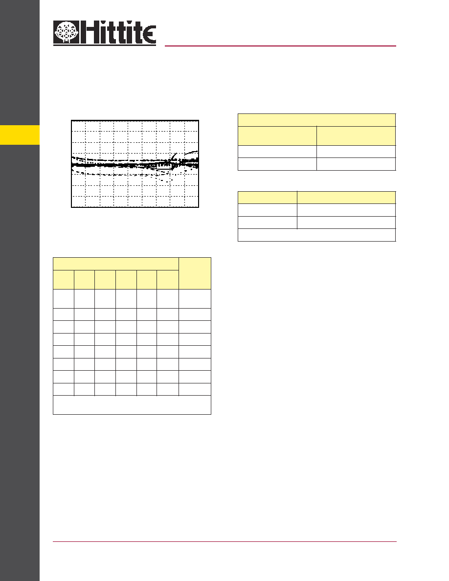
-2
-1.5
-1
-0.5
0
0.5
1
1.5
2
1
2
3
4
5
6
7
8
9
10
STEP ERROR (dB)
FREQUENCY (GHz)
0.5 dB LSB GaAs MMIC 6-BIT DIGITAL
POSITIVE CONTROL ATTENUATOR, 2.4 - 8.0 GHz
Worst Case Step Error
Between Successive Attenuation States
Vdd Range = 3.0 to +5.0 Vdc
Vdd
(VDC)
Idd (Typ.)
(µA)
+3.0
10
+5.0
30
State
Bias Condition
Low
0 to 0.2V @ 10 uA Typ.
High
Vdd ± 0.2V @ 5 uA Typ.
Note: Vdd = +3V to +5V
Control Voltage Input
Attenuation
State
RF1 - RF2
V1
16 dB
V2
8 dB
V3
4 dB
V4
2 dB
V5
1 dB
V6
0.5 dB
High
High
High
High
High
High
Reference
I.L.
High
High
High
High
High
Low
0.5 dB
High
High
High
High
Low
High
1 dB
High
High
High
Low
High
High
2 dB
High
High
Low
High
High
High
4 dB
High
Low
High
High
High
High
8 dB
Low
High
High
High
High
High
16 dB
Low
Low
Low
Low
Low
Low
31.5 dB
Any combination of the above states will provide an attenuation
approximately equal to the sum of the bits selected.
MICROWAVE CORPORATION
9 - 95
For price, delivery, and to place orders, please contact Hittite Microwave Corporation:
12 Elizabeth Drive, Chelmsford, MA 01824 Phone: 978-250-3343 Fax: 978-250-3373
Order Online at www.hittite.com
A
TTENU
A
T
ORS - SMT
9
Absolute Maximum Ratings
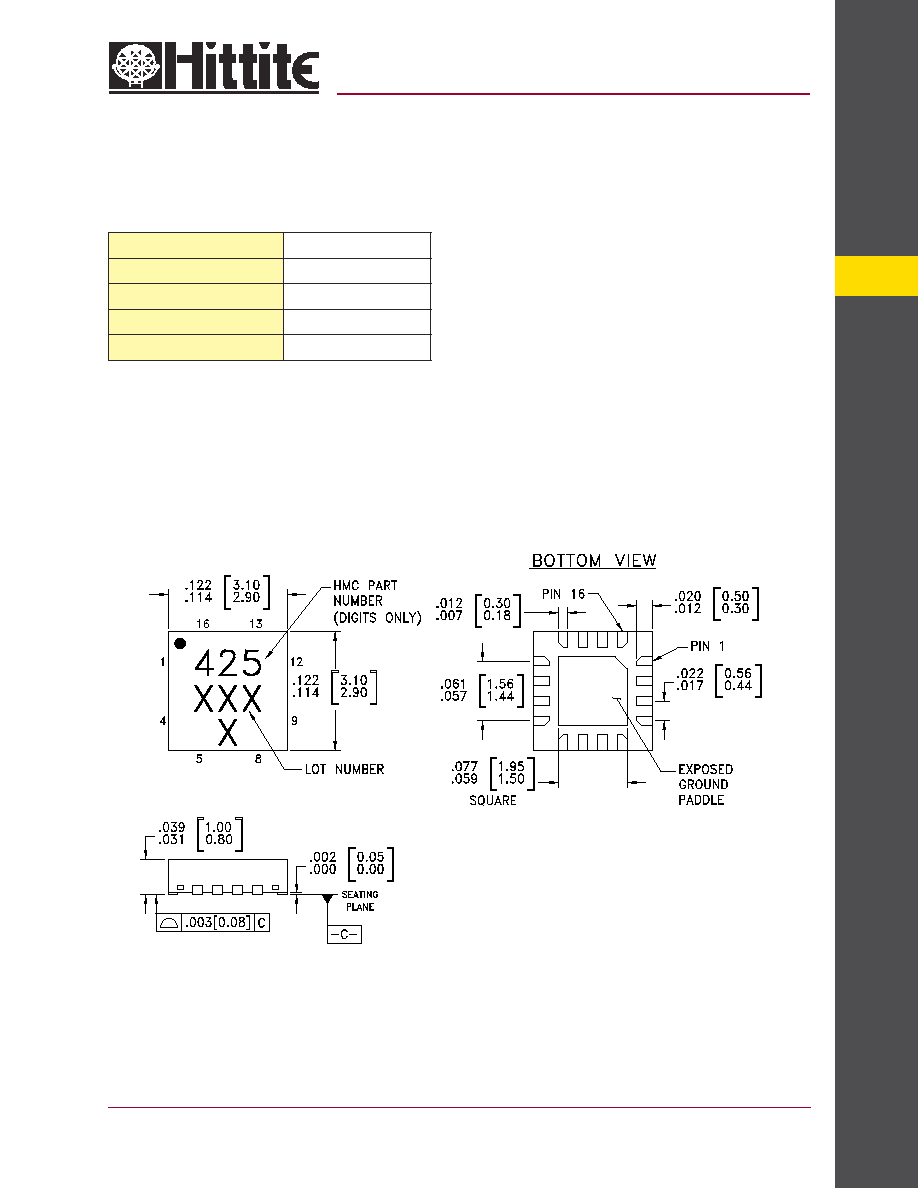
Outline Drawing
HMC425LP3
v00.0202
0.5 dB LSB GaAs MMIC 6-BIT DIGITAL
POSITIVE CONTROL ATTENUATOR, 2.4 - 8.0 GHz
Control Voltage (V1 to V6)
Vdd +0.5 Vdc
Bias Voltage (Vdd)
+7.0 Vdc
Staorage Temperature
-65 to +150 °C
Operating Temperature
-40 to +85 °C
RF Input Power (2.4 - 8.0 GHz)
+30 dBm
NOTES:
1. MATERIAL PACKAGE BODY: LOW STRESS INJECTION MOLDED
PLASTIC SILICA AND SILICON IMPREGNATED.
2. LEAD AND GROUND PADDLE MATERIAL: COPPER ALLOY
3. LEAD AND GROUND PADDLE PLATING: Sn/Pb SOLDER
4. DIMENSIONS ARE IN INCHES [MILLIMETERS].
5. LEAD SPACING TOLERANCE IS NON-CUMULATIVE
6. PAD BURR LENGTH SHALL BE 0.15mm MAXIMUM.
PAD BURR HEIGHT SHALL BE 0.05mm MAXIMUM.
7. PACKAGE WARP SHALL NOT EXCEED 0.05mm.
8. ALL GROUND LEADS AND GROUND PADDLE MUST BE SOLDERED
TO PCB RF GROUND.
MICROWAVE CORPORATION
9 - 96
For price, delivery, and to place orders, please contact Hittite Microwave Corporation:
12 Elizabeth Drive, Chelmsford, MA 01824 Phone: 978-250-3343 Fax: 978-250-3373
Order Online at www.hittite.com
A
TTENU
A
T
ORS - SMT
9
HMC425LP3
v00.0202
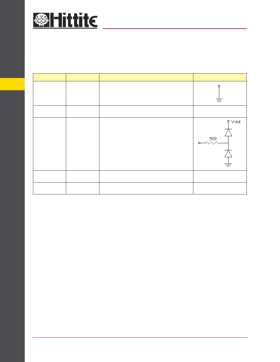
Pin Descriptions
0.5 dB LSB GaAs MMIC 6-BIT DIGITAL
POSITIVE CONTROL ATTENUATOR, 2.4 - 8.0 GHz
Pin Number
Function
Description
Interface Schematic
1, 3, 10, 12
GND
Package bottom has an exposed metal paddle that must also
be connected to RF Ground.
2, 11
RFIN, RFOUT
This pin is DC coupled and matched to 50 Ohm.
Blocking capacitors are required.
4, 5, 6, 7, 8, 9
V1 - V6
See truth table and control voltage table.
13, 14, 16
N/C
This pin should be connected to PCB RF ground to
maximize performance.
15
Vdd
Supply Voltage.