 | ÐлекÑÑоннÑй компоненÑ: HMC462 | СкаÑаÑÑ:  PDF PDF  ZIP ZIP |
Äîêóìåíòàöèÿ è îïèñàíèÿ www.docs.chipfind.ru
MICROWAVE CORPORATION
1 - 76
For price, delivery, and to place orders, please contact Hittite Microwave Corporation:
12 Elizabeth Drive, Chelmsford, MA 01824 Phone: 978-250-3343 Fax: 978-250-3373
Order Online at www.hittite.com
AMPLIFIERS - CHIP
1
HMC462
GaAs PHEMT MMIC
LOW NOISE AMPLIFIER, 2.0 - 20.0 GHz
v00.0703
General Description
Features
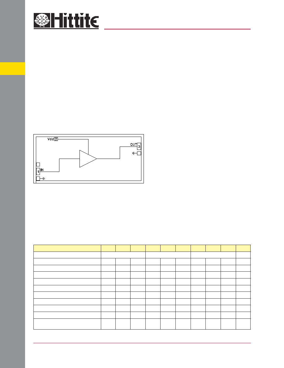
Functional Diagram
The HMC462 is a GaAs MMIC PHEMT Low Noise
Distributed Amplifi er die which operates between 2
and 20 GHz. The amplifi er provides 15 dB of gain,
2.0 to 2.5 dB noise fi gure and +15 dBm of output
power at 1 dB gain compression while requiring
only 63 mA from a single +5V supply. Gain fl atness
is excellent at ±0.5 dB from 6 - 18 GHz making the
HMC462 ideal for EW, ECM and RADAR applica-
tions. The HMC462 requires a single supply of
+5V @ 63 mA and is the self-biased version of the
HMC463. The wideband amplifi er I/Os are inter-
nally matched to 50 Ohms facilitating easy integra-
tion into Multi-Chip-Modules (MCMs). All data is
with the chip in a 50 Ohm test fi xture connected
via 0.025mm (1 mil) diameter wire bonds of minimal
length 0.31mm (12 mils).
Noise Figure: 2 dB @ 10 GHz
Gain: 15 dB
P1dB Output Power: +15 dBm @ 10 GHz
Self-Biased: +5.0V @ 63 mA
50 Ohm Matched Input/Output
3.12 mm x 1.38 mm x 0.1 mm
Typical Applications
The HMC462 Wideband LNA is ideal for:
· Telecom Infrastructure
· Microwave Radio & VSAT
· Military & Space
· Test Instrumentation
· Fiber Optics
Electrical Specifi cations,
T
A
= +25° C, Vdd= 5V
Parameter
Min.
Typ.
Max.
Min.
Typ.
Max.
Min.
Typ.
Max.
Units
Frequency Range
2.0 - 6.0
6.0 - 18.0
18.0 - 20.0
GHz
Gain
13.5
15.5
13
15
12
14
dB
Gain Flatness
±0.5
±0.5
±0.5
dB
Gain Variation Over Temperature
0.015
0.025
0.015
0.025
0.015
0.025
dB/ °C
Noise Figure
3.0
4.0
2.5
3.5
3.0
3.7
dB
Input Return Loss
15
20
14
dB
Output Return Loss
12
13
8
dB
Output Power for 1 dB Compression (P1dB)
12.5
15.5
11
14
9.5
12.5
dBm
Saturated Output Power (Psat)
18
16
15.5
dBm
Output Third Order Intercept (IP3)
26.5
25.5
24
dBm
Supply Current
(Idd) (Vdd= 5V)
63
63
63
mA
MICROWAVE CORPORATION
1 - 77
For price, delivery, and to place orders, please contact Hittite Microwave Corporation:
12 Elizabeth Drive, Chelmsford, MA 01824 Phone: 978-250-3343 Fax: 978-250-3373
Order Online at www.hittite.com
AMPLIFIERS - CHIP
1
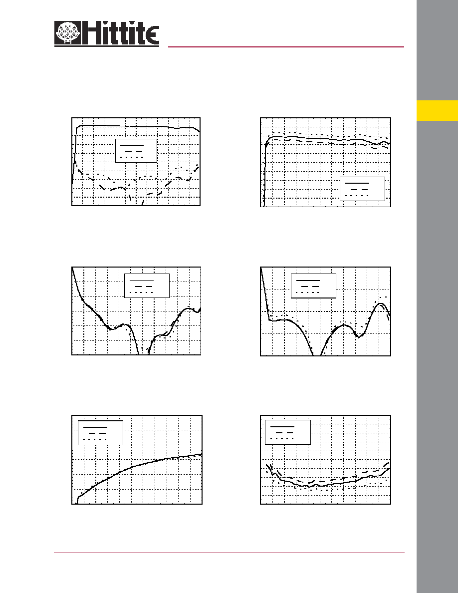
Noise Figure vs. Temperature
GaAs PHEMT MMIC
LOW NOISE AMPLIFIER, 2.0 - 20.0 GHz
Gain vs. Temperature
Output Return Loss vs. Temperature
HMC462
v00.0703
Gain & Return Loss
Reverse Isolation vs. Temperature
Input Return Loss vs. Temperature
0
2
4
6
8
10
12
14
16
18
20
0
2
4
6
8
10
12
14
16
18
20
22
+25C
+85C
-40C
GAIN
(dB)
FREQUENCY (GHz)
-20
-15
-10
-5
0
0
2
4
6
8
10
12
14
16
18
20
22
+25C
+85C
-40C
OUTPUT RETURN LOSS (dB)
FREQUENCY (GHz)
-60
-50
-40
-30
-20
-10
0
0
2
4
6
8
10
12
14
16
18
20
22
+25C
+85C
-40C
REVERSE ISOLATION (dB)
FREQUENCY (GHz)
0
1
2
3
4
5
6
7
8
9
10
0
2
4
6
8
10
12
14
16
18
20
22
+25C
+85C
-40C
NOI
SE FI
GURE (dB)
FREQUENCY (GHz)
-30
-25
-20
-15
-10
-5
0
5
10
15
20
0
2
4
6
8
10
12
14
16
18
20
22
24
S21
S11
S22
RESPONSE (dB)
FREQUENCY (GHz)
-30
-25
-20
-15
-10
-5
0
0
2
4
6
8
10
12
14
16
18
20
22
+25C
+85C
-40C
INPUT RETURN LOSS (dB)
FREQUENCY (GHz)
MICROWAVE CORPORATION
1 - 78
For price, delivery, and to place orders, please contact Hittite Microwave Corporation:
12 Elizabeth Drive, Chelmsford, MA 01824 Phone: 978-250-3343 Fax: 978-250-3373
Order Online at www.hittite.com
AMPLIFIERS - CHIP
1
HMC462
v00.0703
GaAs PHEMT MMIC
LOW NOISE AMPLIFIER, 2.0 - 20.0 GHz
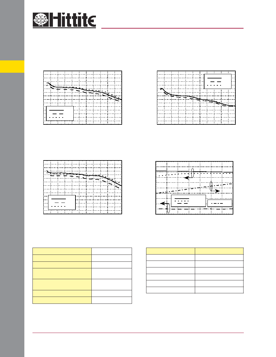
GaAs MMIC SUB-HARMONICALLY PUMPED MIXER 17 - 25 GHz
P1dB vs. Temperature
Psat vs. Temperature
Output IP3 vs. Temperature
Gain, Power, Noise Figure & Supply
Current vs. Supply Voltage @ 10 GHz
5
6
7
8
9
10
11
12
13
14
15
16
17
18
19
20
0
2
4
6
8
10
12
14
16
18
20
22
+25C
+85C
-40C
P1dB (dBm)
FREQUENCY (GHz)
10
11
12
13
14
15
16
17
18
19
20
21
22
23
24
25
0
2
4
6
8
10
12
14
16
18
20
22
+25C
+85C
-55C
Psat (dBm)
FREQUENCY (GHz)
15
16
17
18
19
20
21
22
23
24
25
26
27
28
29
30
0
2
4
6
8
10
12
14
16
18
20
22
+25C
+85C
-40C
OIP3 (dBm)
FREQUENCY (GHz)
0
2
4
6
8
10
12
14
16
18
20
54
56
58
60
62
64
66
68
70
72
74
4.5
5
5.5
6
6.5
7
7.5
8
Gain
P1dB
Noise Figure
Idd
GAIN (dB), P1dB (dBm), NOISE FIGURE (dB)
Idd (mA)
Vdd SUPPLY VOLTAGE (Vdc)
Absolute Maximum Ratings
Drain Bias Voltage (Vdd)
+9.0 Vdc
RF Input Power (RFin)(Vdd = +5.0 Vdc)
+23 dBm
Channel Temperature
175 °C
Continuous Pdiss (T = 85 °C)
(derate 50 mW/°C above 85 °C)
4.5 W
Thermal Resistance
(channel to die bottom)
20 °C/W
Storage Temperature
-65 to +150 °C
Operating Temperature
-55 to +85 °C
Vdd (V)
Idd (mA)
+4.5
62
+5.0
63
+5.5
64
+7.0
65
+7.5
66
+8.0
67
Typical Supply Current vs. Vdd
MICROWAVE CORPORATION
1 - 79
For price, delivery, and to place orders, please contact Hittite Microwave Corporation:
12 Elizabeth Drive, Chelmsford, MA 01824 Phone: 978-250-3343 Fax: 978-250-3373
Order Online at www.hittite.com
AMPLIFIERS - CHIP
1
HMC462
v00.0703
GaAs PHEMT MMIC
LOW NOISE AMPLIFIER, 2.0 - 20.0 GHz
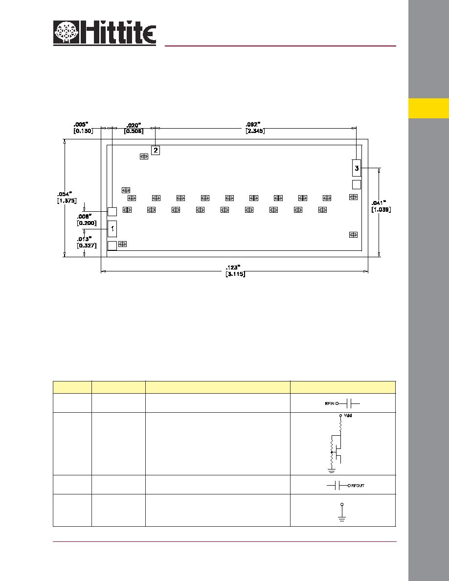
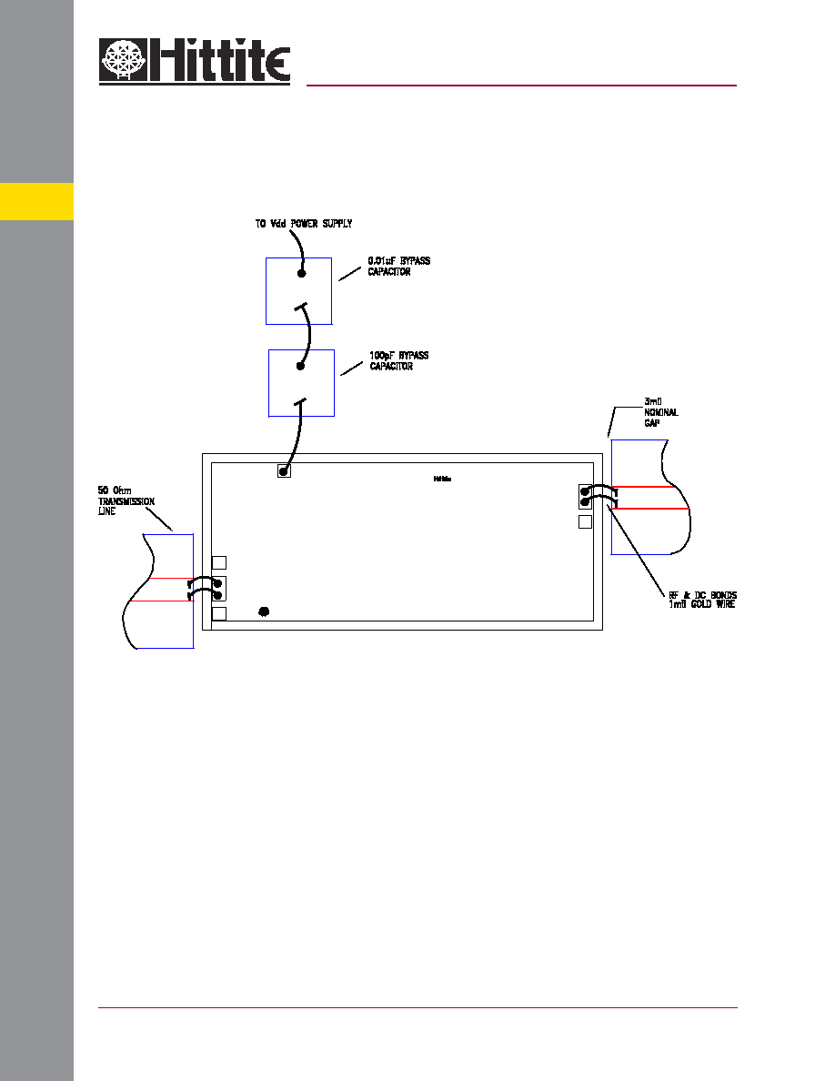
Outline Drawing
NOTES:
1. ALL DIMENSIONS IN INCHES [MILLIMETERS]
2. NO CONNECTION REQUIRED FOR UNLABELED BOND PADS
3. DIE THICKNESS IS 0.004 (0.100)
4. TYPICAL BOND PAD IS 0.004 (0.100) SQUARE
5. BACKSIDE METALLIZATION: GOLD
6. BACKSIDE METAL IS GROUND
7. BOND PAD METALIZATION: GOLD
Pad Number
Function
Description
Interface Schematic
1
RFIN
This pad is AC coupled and matched to 50 Ohms
from 2.0 - 20.0 GHz
2
Vdd
Power supply voltage for the amplifi er.
External bypass capacitors are required
3
RFOUT
This pad is AC coupled and matched to 50 Ohms
from 2.0 - 20.0 GHz
Die
Bottom
GND
Die bottom must be connected to RF/DC ground.
Pad Descriptions
MICROWAVE CORPORATION
1 - 80
For price, delivery, and to place orders, please contact Hittite Microwave Corporation:
12 Elizabeth Drive, Chelmsford, MA 01824 Phone: 978-250-3343 Fax: 978-250-3373
Order Online at www.hittite.com
AMPLIFIERS - CHIP
1
HMC462
v00.0703
GaAs PHEMT MMIC
LOW NOISE AMPLIFIER, 2.0 - 20.0 GHz
Assembly Diagram