 | –≠–ª–µ–∫—Ç—Ä–æ–Ω–Ω—ã–π –∫–æ–º–ø–æ–Ω–µ–Ω—Ç: HMC516LC5 | –°–∫–∞—á–∞—Ç—å:  PDF PDF  ZIP ZIP |

8
A
M
P
L
IF
IE
RS
-
S
M
T
8 - 458
For price, delivery, and to place orders, please contact Hittite Microwave Corporation:
20 Alpha Road, Chelmsford, MA 01824 Phone: 978-250-3343 Fax: 978-250-3373
Order On-line at www.hittite.com
HMC516LC5
SMT PHEMT LOW NOISE
AMPLIFIER, 9 - 18 GHz
v00.1204
General Description
Features
Functional Diagram
The HMC516LC5 is a high dynamic range
GaAs PHEMT MMIC Low Noise Amplifi er (LNA)
housed in a leadless "Pb free" RoHS compliant
SMT package. The HMC516LC5 provides 20 dB
of small signal gain, 2.0 dB of noise fi gure and
has an output IP3 of +25 dBm. The P1dB output
power of +13 dBm enables the LNA to also
function as a LO driver for balanced, I/Q or image
reject mixers. The HMC516LC5 allows the use of
surface mount manufacturing techniques.
Noise Figure: 2.0 dB
Gain: 20 dB
OIP3: +25 dBm
Single Supply: +3V @ 65 mA
50 Ohm Matched Input/Output
RoHS Compliant 5 X 5 mm Package
Electrical Specifi cations,
T
A
= +25∞ C, Vdd 1, 2, 3 = +3V
Typical Applications
The HMC516LC5 is ideal for use as a LNA or
driver amplifi er for:
∑ Point-to-Point Radios
∑ Point-to-Multi-Point Radios & VSAT
∑ Test Equipment and Sensors
∑ Military
Parameter
Min.
Typ.
Max.
Min.
Typ.
Max.
Units
Frequency Range
9 - 12
12 - 18
GHz
Gain
17.5
20
18
20.5
dB
Gain Variation Over Temperature
0.015
0.025
0.015
0.025
dB/ ∞C
Noise Figure
2.0
2.5
2.0
2.5
dB
Input Return Loss
10
10
dB
Output Return Loss
12
12
dB
Output Power for 1 dB Compression (P1dB)
13
14
dBm
Saturated Output Power (Psat)
15
16
dBm
Output Third Order Intercept (IP3)
25
25
dBm
Supply Current (Idd)(Vdd = +3V)
65
65
mA
8
A
M
P
L
IF
IE
RS
-
S
M
T
8 - 459
For price, delivery, and to place orders, please contact Hittite Microwave Corporation:
20 Alpha Road, Chelmsford, MA 01824 Phone: 978-250-3343 Fax: 978-250-3373
Order On-line at www.hittite.com
GaAs MMIC SUB-HARMONICALLY PUMPED MIXER 17 - 25 GHz
HMC516LC5
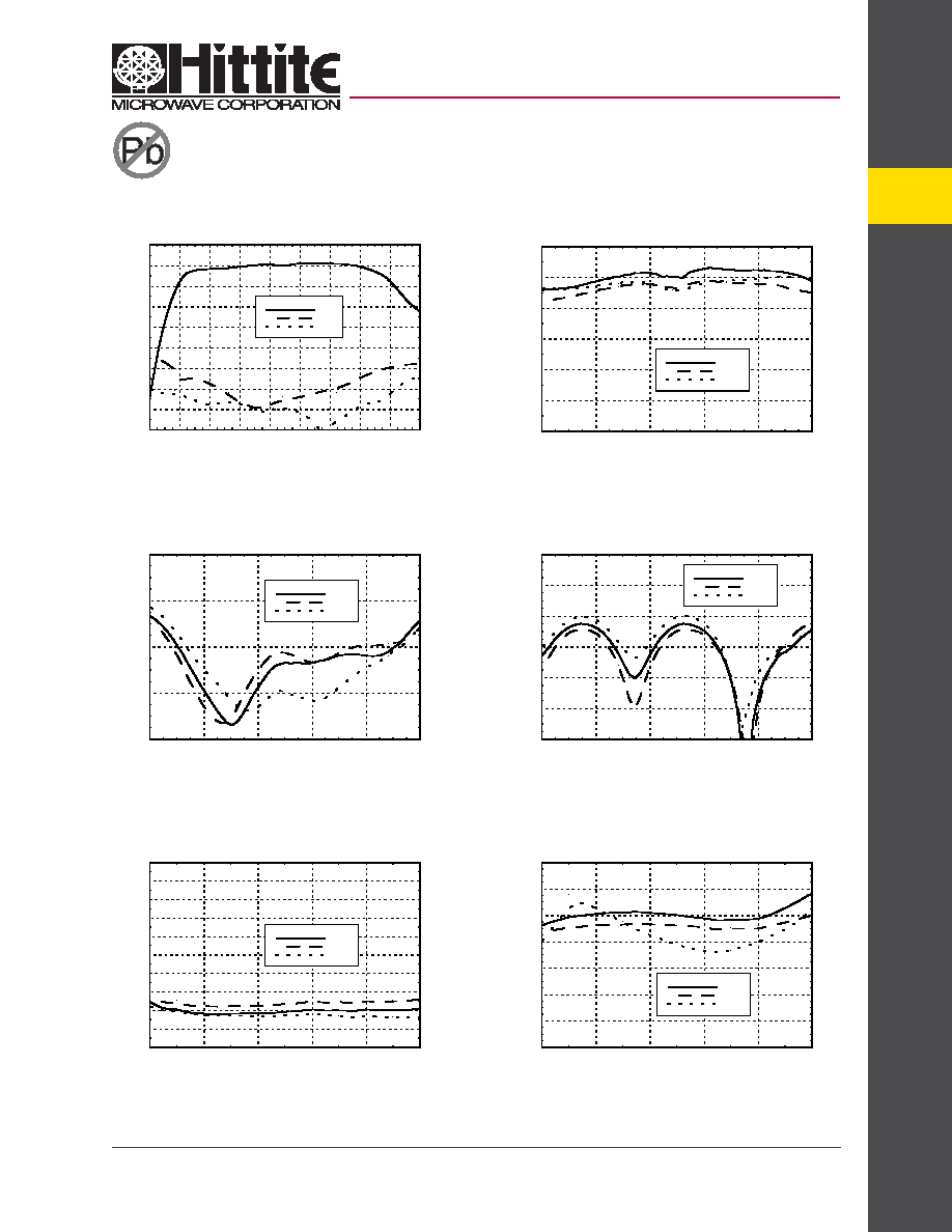
Input Return Loss vs. Temperature
Output Return Loss vs. Temperature
SMT PHEMT LOW NOISE
AMPLIFIER, 9 - 18 GHz
v00.1204
Broadband Gain & Return Loss
Gain vs. Temperature
Noise Figure vs. Temperature
Output IP3 vs. Temperature
-20
-15
-10
-5
0
5
10
15
20
25
4
6
8
10
12
14
16
18
20
22
S21
S11
S22
RESPONSE (dB)
FREQUENCY (GHz)
10
12
14
16
18
20
22
8
10
12
14
16
18
+25C
+85C
-40C
GAIN
(dB)
FREQUENCY (GHz)
-20
-15
-10
-5
0
8
10
12
14
16
18
+25C
+85C
-40C
RETURN LOSS (dB)
FREQUENCY (GHz)
-30
-25
-20
-15
-10
-5
0
8
10
12
14
16
18
+25C
+85C
-40C
RETURN LOSS (dB)
FREQUENCY (GHz)
0
1
2
3
4
5
6
7
8
9
10
8
10
12
14
16
18
+25C
+85C
-40C
NOI
SE FI
GURE (dB)
FREQUENCY (GHz)
0
5
10
15
20
25
30
35
8
10
12
14
16
18
+25C
+85C
-40C
OIP3 (dBm)
FREQUENCY (GHz)

8
A
M
P
L
IF
IE
RS
-
S
M
T
8 - 460
For price, delivery, and to place orders, please contact Hittite Microwave Corporation:
20 Alpha Road, Chelmsford, MA 01824 Phone: 978-250-3343 Fax: 978-250-3373
Order On-line at www.hittite.com
HMC516LC5
SMT PHEMT LOW NOISE
AMPLIFIER, 9 - 18 GHz
v00.1204
P1dB vs. Temperature
Power Compression @ 12 GHz
Reverse Isolation vs. Temperature
Psat vs. Temperature
Gain, Noise Figure & Power vs.
Supply Voltage @ 12 GHz
0
2
4
6
8
10
12
14
16
18
20
8
10
12
14
16
18
+25C
+85C
-40C
P1dB (dBm)
FREQUENCY (GHz)
0
2
4
6
8
10
12
14
16
18
20
8
10
12
14
16
18
+25C
+85C
-40C
Psat (dBm)
FREQUENCY (GHz)
-80
-70
-60
-50
-40
-30
-20
-10
0
8
10
12
14
16
18
+25C
+85C
-40C
ISOLATION (dB)
FREQUENCY (GHz)
0
5
10
15
20
25
-22
-20
-18
-16
-14
-12
-10
-8
-6
-4
-2
0
Pout
Gain
PAE
Pout (dBm), GAIN (dB), PAE (%)
INPUT POWER (dBm)
10
12
14
16
18
20
22
24
0
1
2
3
4
5
6
7
2.5
3
3.5
GAIN (dB), P1dB (dBm)
NOI
SE FI
GURE (dB)
Vdd (Vdc)
Noise Figure
P1dB
Gain

8
A
M
P
L
IF
IE
RS
-
S
M
T
8 - 461
For price, delivery, and to place orders, please contact Hittite Microwave Corporation:
20 Alpha Road, Chelmsford, MA 01824 Phone: 978-250-3343 Fax: 978-250-3373
Order On-line at www.hittite.com
HMC516LC5
SMT PHEMT LOW NOISE
AMPLIFIER, 9 - 18 GHz
v00.1204
Outline Drawing
Absolute Maximum Ratings
Drain Bias Voltage (Vdd1, Vdd2,
Vdd3)
+4 Vdc
RF Input Power (RFin)(Vdd = +3.0
Vdc)
+10 dBm
Channel Temperature
175 ∞C
Continuous Pdiss (T= 85 ∞C)
(derate 14 mW/∞C above 85 ∞C)
1.25 W
Thermal Resistance
(channel to die bottom)
71 ∞C/W
Storage Temperature
-65 to +150 ∞C
Operating Temperature
-40 to +85 ∞C
ESD Sensitivity (HBM)
Class 1A
Vdd (Vdc)
Idd (mA)
+2.5
61
+3.0
65
+3.5
69
Typical Supply Current vs. Vdd
Note: Amplifi er will operate over full voltage range
shown above.
NOTES:
1. PACKAGE BODY MATERIAL: ALUMINA
2. LEAD AND GROUND PADDLE PLATING: 30-80 MICROINCHES
GOLD OVER 50 MICROINCHES MINIMUM NICKEL
3. DIMENSIONS ARE IN INCHES [MILLIMETERS]
4. LEAD SPACING TOLERANCE IS NON-CUMULATIVE
5. PACKAGE WARP SHALL NOT EXCEED 0.05mm DATUM
6. ALL GROUND LEADS AND GROUND PADDLE MUST BE
SOLDERED TO PCB RF GROUND
ELECTROSTATIC SENSITIVE DEVICE
OBSERVE HANDLING PRECAUTIONS

8
A
M
P
L
IF
IE
RS
-
S
M
T
8 - 462
For price, delivery, and to place orders, please contact Hittite Microwave Corporation:
20 Alpha Road, Chelmsford, MA 01824 Phone: 978-250-3343 Fax: 978-250-3373
Order On-line at www.hittite.com
HMC516LC5
SMT PHEMT LOW NOISE
AMPLIFIER, 9 - 18 GHz
v00.1204
Pin Descriptions
Pin Number
Function
Description
Interface Schematic
1, 2, 6-19,
23-25, 27,
29, 31, 32
N/C
This pin may be connected to RF/DC ground.
Performance will not be affected.
4
RFIN
This pin is AC coupled and matched to 50 Ohms from
9 - 18 GHz.
30, 28, 26
Vdd1, 2, 3
Power Supply Voltage for the amplifi er. External bypass
capacitors of 100 pF and 2.2 µF are required.
21
RFOUT
This pin is AC coupled and matched to 50 Ohms from
9 - 18 GHz.
3, 5, 20, 22
GND
These pins and package bottom must be
connected to RF/DC ground.
Application Circuit
Component
Value
C1, C2, C3
100 pF
C4, C5, C6
2.2 µF