 | ÐлекÑÑоннÑй компоненÑ: HMC519 | СкаÑаÑÑ:  PDF PDF  ZIP ZIP |
untitled
1 - 168
For price, delivery, and to place orders, please contact Hittite Microwave Corporation:
20 Alpha Road Chelmsford, MA 01824 Phone: 978-250-3343 Fax: 978-250-3373
Order Online at www.hittite.com
AMPLIFIERS - CHIP
1
HMC519
GaAs PHEMT MMIC LOW NOISE
AMPLIFIER, 18 - 32 GHz
v00.0904
General Description
Features
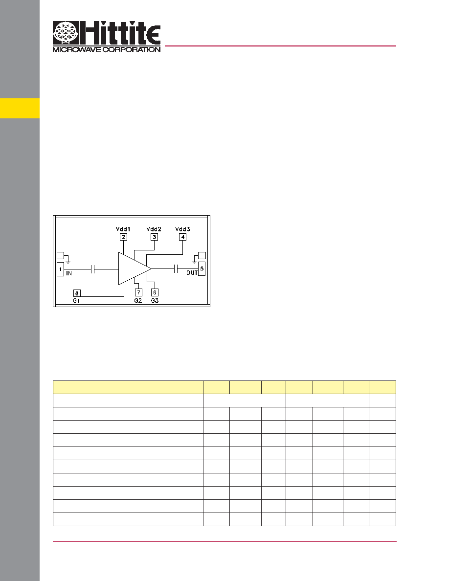
Functional Diagram
The HMC519 chip is a high dynamic range GaAs
PHEMT MMIC Low Noise Amplifi er (LNA) which
covers the 18 to 32 Ghz frequency range. The
HMC519 provides 15 dB of small signal gain,
2.8 dB of noise fi gure and has an output IP3
greater than 23 dBm. The chip can easily be
integrated into hybrid or MCM assemblies due to
its small size. All data is tested with the chip in a
50 Ohm test fi xture connected via 0.075 mm (3
mil) ribbon bonds of minimal length 0.31 mm (12
mil). Two 0.025 mm (1 mil) diameter bondwires
may also be used to make the RFIN and RFOUT
connections.
Noise Figure: 2.8 dB
Gain: 15 dB
OIP3: 23 dBm
Single Supply: +3V @ 65 mA
50 Ohm Matched Input/Output
Electrical Specifi cations,
T
A
= +25° C, Vdd 1, 2, 3 = +3V
Typical Applications
The HMC519 is ideal for use as either a LNA or
driver amplifi er for:
· Point-to-Point Radios
· Point-to-Multi-Point Radios & VSAT
· Test Equipment & Sensors
· Military & Space
Parameter
Min.
Typ.
Max.
Min.
Typ.
Max.
Units
Frequency Range
18 - 28
28 - 32
GHz
Gain
12
15
11
14
dB
Gain Variation Over Temperature
0.015
0.025
0.015
0.025
dB/ °C
Noise Figure
2.8
3.5
3.5
4.5
dB
Input Return Loss
13
9
dB
Output Return Loss
12
12
dB
Output Power for 1 dB Compression (P1dB)
9
12
10
14
dBm
Saturated Output Power (Psat)
15
18
dBm
Output Third Order Intercept (IP3)
23
26
dBm
Supply Current (Idd)(Vdd = +3V)
65
65
mA
1 - 169
For price, delivery, and to place orders, please contact Hittite Microwave Corporation:
20 Alpha Road Chelmsford, MA 01824 Phone: 978-250-3343 Fax: 978-250-3373
Order Online at www.hittite.com
AMPLIFIERS - CHIP
1
GaAs MMIC SUB-HARMONICALLY PUMPED MIXER 17 - 25 GHz
HMC519
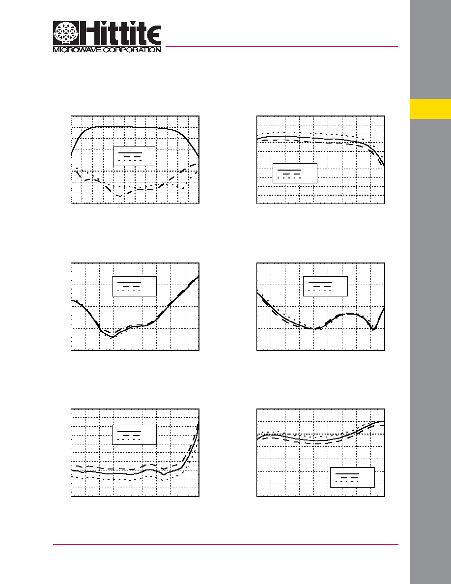
Input Return Loss vs. Temperature
Output Return Loss vs. Temperature
GaAs PHEMT MMIC LOW NOISE
AMPLIFIER, 18 - 32 GHz
v00.0904
Broadband Gain & Return Loss
Gain vs. Temperature
Noise Figure vs. Temperature
Output IP3 vs. Temperature
-20
-15
-10
-5
0
5
10
15
20
12
14
16
18
20
22
24
26
28
30
32
34
36
S21
S11
S22
RESPONSE (dB)
FREQUENCY (GHz)
0
2
4
6
8
10
12
14
16
18
20
16
18
20
22
24
26
28
30
32
34
+25C
+85C
-55C
GAIN
(dB)
FREQUENCY (GHz)
-20
-15
-10
-5
0
16
18
20
22
24
26
28
30
32
34
+25C
+85C
-55C
RETURN LOSS (dB)
FREQUENCY (GHz)
-20
-15
-10
-5
0
16
18
20
22
24
26
28
30
32
34
+25C
+85C
-55C
RETURN LOSS (dB)
FREQUENCY (GHz)
0
1
2
3
4
5
6
7
8
9
10
16
18
20
22
24
26
28
30
32
34
+25C
+85C
-55C
NOI
SE FI
GURE (dB)
FREQUENCY (GHz)
0
5
10
15
20
25
30
35
16
18
20
22
24
26
28
30
32
34
+25C
+85C
-55C
OIP3 (dBm)
FREQUENCY (GHz)
1 - 170
For price, delivery, and to place orders, please contact Hittite Microwave Corporation:
20 Alpha Road Chelmsford, MA 01824 Phone: 978-250-3343 Fax: 978-250-3373
Order Online at www.hittite.com
AMPLIFIERS - CHIP
1
HMC519
GaAs PHEMT MMIC LOW NOISE
AMPLIFIER, 18 - 32 GHz
v00.0904
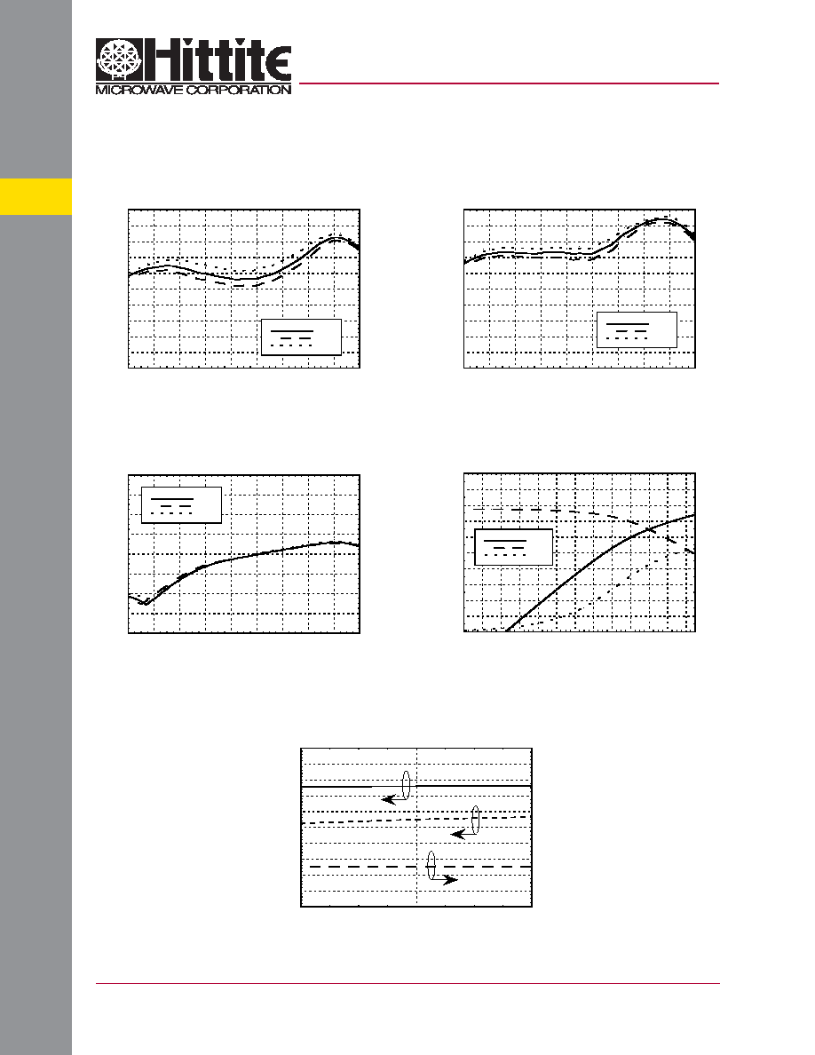
P1dB vs. Temperature
Power Compression @ 24 GHz
Reverse Isolation vs. Temperature
Psat vs. Temperature
0
2
4
6
8
10
12
14
16
18
20
16
18
20
22
24
26
28
30
32
34
+25C
+85C
-55C
P1dB (dBm)
FREQUENCY (GHz)
0
2
4
6
8
10
12
14
16
18
20
16
18
20
22
24
26
28
30
32
34
+25C
+85C
-55C
Psat (dBm)
FREQUENCY (GHz)
-80
-70
-60
-50
-40
-30
-20
-10
0
16
18
20
22
24
26
28
30
32
34
+25C
+85C
-55C
ISOLATION (dB)
FREQUENCY (GHz)
0
2
4
6
8
10
12
14
16
18
20
-20 -18 -16 -14 -12 -10
-8
-6
-4
-2
0
2
4
Pout
Gain
PAE
Pout (dBm), GAIN (dB), PAE (%)
INPUT POWER (dBm)
Gain, Noise Figure & Power vs.
Supply Voltage @ 24 GHz
0
2
4
6
8
10
12
14
16
18
20
0
1
2
3
4
5
6
7
8
9
10
2.5
3
3.5
GAIN (dB), P1dB (dBm)
NOI
SE FI
GURE (dB)
Vdd (Vdc)
Gain
P1dB
Noise Figure
1 - 171
For price, delivery, and to place orders, please contact Hittite Microwave Corporation:
20 Alpha Road Chelmsford, MA 01824 Phone: 978-250-3343 Fax: 978-250-3373
Order Online at www.hittite.com
AMPLIFIERS - CHIP
1
HMC519
GaAs PHEMT MMIC LOW NOISE
AMPLIFIER, 18 - 32 GHz
v00.0904
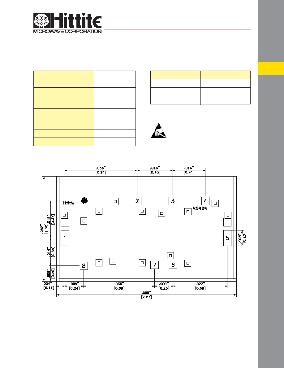
Outline Drawing
Absolute Maximum Ratings
Drain Bias Voltage (Vdd1, Vdd2, Vdd3)
+5.5 Vdc
RF Input Power (RFin)(Vdd = +3.0 Vdc)
+10 dBm
Channel Temperature
175 °C
Continuous Pdiss (T= 85 °C)
(derate 29 mW/°C above 85 °C)
2.65 W
Thermal Resistance
(channel to die bottom)
34 °C/W
Storage Temperature
-65 to +150 °C
Operating Temperature
-55 to +85 °C
ESD Sensitivity (HBM)
Class 1A
Vdd (Vdc)
Idd (mA)
+2.5
61
+3.0
65
+3.5
69
Typical Supply Current vs. Vdd
Note: Amplifi er will operate over full voltage ranges
shown above.
NOTES:
1. ALL DIMENSIONS ARE IN INCHES [MM]
2. DIE THICKNESS IS .004"
3. TYPICAL BOND IS .004" SQUARE
4. BACKSIDE METALLIZATION: GOLD
5. BOND PAD METALLIZATION: GOLD
6. BACKSIDE METAL IS GROUND.
7. CONNECTION NOT REQUIRED FOR UNLABELED BOND PADS.
ELECTROSTATIC SENSITIVE DEVICE
OBSERVE HANDLING PRECAUTIONS
1 - 172
For price, delivery, and to place orders, please contact Hittite Microwave Corporation:
20 Alpha Road Chelmsford, MA 01824 Phone: 978-250-3343 Fax: 978-250-3373
Order Online at www.hittite.com
AMPLIFIERS - CHIP
1
HMC519
GaAs PHEMT MMIC LOW NOISE
AMPLIFIER, 18 - 32 GHz
v00.0904
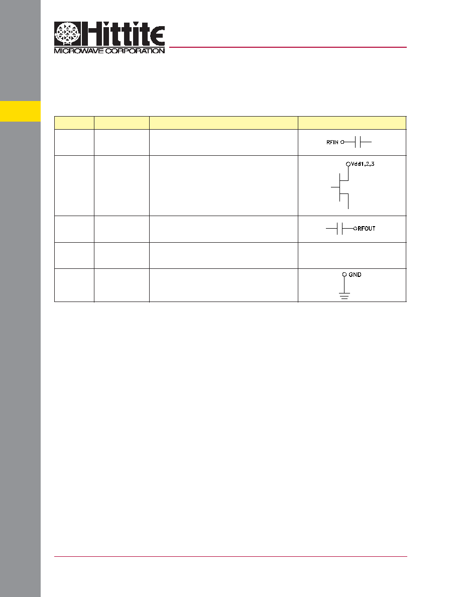
Pad Descriptions
Pad Number
Function
Description
Interface Schematic
1
RF IN
This pad is AC coupled and matched to 50 Ohms from
18 - 32 GHz.
2, 3, 4
Vdd1, 2, 3
Power Supply Voltage for the amplifi er. External bypass
capacitors of 100 pF and 0.1
µ
F are required.
5
RF OUT
This pad is AC coupled and matched to 50 Ohms from
18 - 32 GHz.
6, 7, 8
G3, 2, 1
These pads must be connected to RF/DC ground for proper
operation.
Die Bottom
GND
Die Bottom must be connected to RF/DC ground.