Untitled-1
12
M
I
X
E
R
S
- SM
T
12 - 322
For price, delivery, and to place orders, please contact Hittite Microwave Corporation:
20 Alpha Road, Chelmsford, MA 01824 Phone: 978-250-3343 Fax: 978-250-3373
Order On-line at www.hittite.com
HMC521LC4
GaAs MMIC I/Q MIXER
8.5 - 13.5 GHz
v00.0105
General Description
Features
Typical Applications
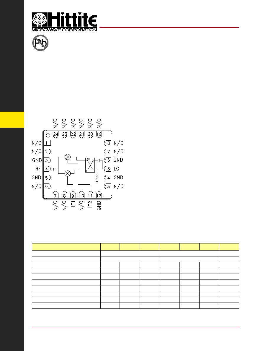
The HMC521LC4 is a compact I /Q MMIC mixer in
a leadless "Pb free" RoHS compliant SMT package,
which can be used as either an Image Reject Mixer
or a Single Sideband Upconverter. The mixer
utilizes two standard Hittite double balanced
mixer cells and a 90 degree hybrid fabricated
in a GaAs MESFET process. A low frequency
quadrature hybrid was used to produce a 100 MHz
USB IF output. This product is a much smaller
alternative to hybrid style Image Reject Mixers and
Single Sideband Upconverter assemblies. The
HMC521LC4 eliminates the need for wire bonding
allowing use of surface mount manufacturing
techniques.
Electrical Specifi cations,
T
A
= +25� C, IF= 100 MHz, LO = +15 dBm*
* Unless otherwise noted, all measurements performed as downconverter.
Parameter
Min.
Typ.
Max.
Min.
Typ.
Max.
Units
Frequency Range, RF/LO
8.5 - 13.5
7.1 - 8.5
GHz
Frequency Range, IF
DC - 3.5
DC - 3.5
GHz
Conversion Loss (As IRM)
8
10
7.5
9.5
dB
Image Rejection
20
30
30
38
dB
1 dB Compression (Input)
+14
+15
dBm
LO to RF Isolation
35
45
45
55
dB
LO to IF Isolation
18
22
20
24
dB
IP3 (Input)
+23
+24
dBm
Amplitude Balance
0.3
0.1
dB
Phase Balance
4
4
Deg
Functional Diagram
The HMC521LC4 is ideal for:
� Point-to-Point and Point-to-Multi-Point Radio
� Military Radar
Wide IF Bandwidth: DC - 3.5 GHz
Image Rejection: 38 dB
LO to RF Isolation: 50 dB
High Input IP3: +23 dBm
RoHS Compliant 4 x 4 mm SMT Package
12
M
I
X
E
R
S
- SM
T
12 - 323
For price, delivery, and to place orders, please contact Hittite Microwave Corporation:
20 Alpha Road, Chelmsford, MA 01824 Phone: 978-250-3343 Fax: 978-250-3373
Order On-line at www.hittite.com
HMC521LC4
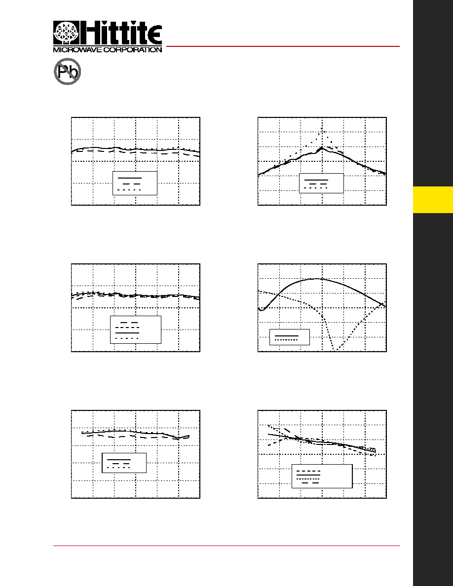
Conversion Gain vs. Temperature
Input P1dB vs. Temperature
Conversion Gain vs. LO Drive
Image Rejection vs. Temperature
Return Loss
Input IP3 vs. LO Drive
Data Taken As IRM With External IF Hybrid
-20
-15
-10
-5
0
8
9
10
11
12
13
14
+25C
+85C
-55C
CONVERSION GAIN (dB)
RF FREQUENCY (GHz)
0
10
20
30
40
50
60
8
9
10
11
12
13
14
+25C
+85C
-55C
I
M
AGE REJECTI
ON (dB)
RF FREQUENCY (GHz)
-20
-15
-10
-5
0
8
9
10
11
12
13
14
+13 dBm
+15 dBm
+17 dBm
+19 dBm
CONVERSION GAIN (dB)
RF FREQUENCY (GHz)
-30
-25
-20
-15
-10
-5
0
8
9
10
11
12
13
14
RF
LO
RETURN LOSS (dB)
FREQUENCY (GHz)
0
4
8
12
16
20
8
9
10
11
12
13
14
+25C
+85C
-55C
P1dB (dBm)
RF FREQUENCY (GHz)
5
10
15
20
25
30
35
8
9
10
11
12
13
14
LO = +13 dBm
LO = +15 dBm
LO = +17 dBm
LO = +19 dBm
IP3 (dBm)
RF FREQUENCY (GHz)
GaAs MMIC I/Q MIXER
8.5 - 13.5 GHz
v00.0105
12
M
I
X
E
R
S
- SM
T
12 - 324
For price, delivery, and to place orders, please contact Hittite Microwave Corporation:
20 Alpha Road, Chelmsford, MA 01824 Phone: 978-250-3343 Fax: 978-250-3373
Order On-line at www.hittite.com
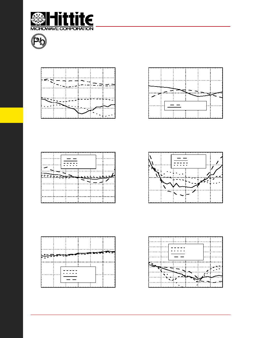
Isolations
IF Bandwidth*
Upconverter Performance Conversion
Gain vs. LO Drive
Amplitude Balance vs. LO Drive
Phase Balance vs. LO Drive
Quadrature Channel Data Taken Without IF Hybrid
Upconverter Performance Sideband
Rejection vs. LO Drive
* Conversion gain data taken with external IF hybrid
-60
-50
-40
-30
-20
-10
8
9
10
11
12
13
14
ISOLATION (dB)
RF FREQUENCY (GHz)
LO/RF
RF/IF1
LO/IF1
RF/IF2
LO/IF2
-20
-15
-10
-5
0
0.5
1
1.5
2
2.5
3
3.5
RETURN LOSS
CONVERSION GAIN
RESPONSE (dB)
IF FREQUENCY (GHz)
-2
-1.5
-1
-0.5
0
0.5
1
1.5
2
8
9
10
11
12
13
14
LO = +13 dBm
LO = +15 dBm
LO = +17 dBm
LO = +19 dBm
AMPLITUDE BALANCE (dB)
RF FREQUENCY (GHz)
-10
-5
0
5
10
8
9
10
11
12
13
14
LO = +13 dBm
LO = +15 dBm
LO = +17 dBm
LO = +19 dBm
PHASE BALANCE (degrees)
RF FREQUENCY (GHz)
-20
-15
-10
-5
0
8
9
10
11
12
13
14
LO = +13 dBm
LO = +17 dBm
LO = +15 dBm
LO = +19 dBm
CONVERSION GAIN (dB)
RF FREQUENCY (GHz)
-50
-40
-30
-20
-10
0
8
9
10
11
12
13
14
LO = +13 dBm
LO = +15 dBm
LO = +17 dBm
LO = +19 dBm
SI
DEBAND REJECTI
ON (dBc)
RF FREQUENCY (GHz)
HMC521LC4
GaAs MMIC I/Q MIXER
8.5 - 13.5 GHz
v00.0105
12
M
I
X
E
R
S
- SM
T
12 - 325
For price, delivery, and to place orders, please contact Hittite Microwave Corporation:
20 Alpha Road, Chelmsford, MA 01824 Phone: 978-250-3343 Fax: 978-250-3373
Order On-line at www.hittite.com
Harmonics of LO
LO Freq. (GHz)
nLO Spur at RF Port
1
2
3
4
8.5
42
44
44
70
9.5
50
53
59
77
10.5
51
54
63
xx
11.5
47
58
66
xx
12.5
45
59
70
xx
13.5
45
57
xx
xx
LO = + 15 dBm
Values in dBc below input LO level measured at RF Port.
MxN Spurious Outputs
nLO
mRF
0
1
2
3
4
0
xx
-5
29
23
52
1
27
0
51
59
81
2
92
85
76
82
92
3
92
92
92
92
92
4
92
92
92
92
92
RF = 10.6 GHz @ -10 dBm
LO = 10.5 GHz @ +15 dBm
Data taken without IF hybrid
All values in dBc below IF power level
Absolute Maximum Ratings
RF / IF Input
+20 dBm
LO Drive
+ 27 dBm
Channel Temperature
150�C
Continuous Pdiss (T=85�C)
(derate 6.9 mW/�C above 85�C)
460 mW
Thermal Resistance (R
TH
)
(junction to package bottom)
141.4 �C/W
Storage Temperature
-65 to +150 �C
Operating Temperature
-55 to +85 �C
Outline Drawing
NOTES:
1. PACKAGE BODY MATERIAL: ALUMINA
2. LEAD AND GROUND PADDLE PLATING: 30 - 80 MICROINCHES
GOLD OVER 50 MICROINCHES MINIMUM NICKLE
3. DIMENSIONS ARE IN INCHES [MILLIMETERS]
4. LEAD SPACING TOLERANCE IS NON-CUMULATIVE
5. PACKAGE WARP SHALL NOT EXCEED 0.05mm DATUM
6. ALL GROUND LEADS AND GROUND PADDLE MUST BE SOLDERED
TO PCB RF GROUND
HMC521LC4
GaAs MMIC I/Q MIXER
8.5 - 13.5 GHz
v00.0105
12
M
I
X
E
R
S
- SM
T
12 - 326
For price, delivery, and to place orders, please contact Hittite Microwave Corporation:
20 Alpha Road, Chelmsford, MA 01824 Phone: 978-250-3343 Fax: 978-250-3373
Order On-line at www.hittite.com
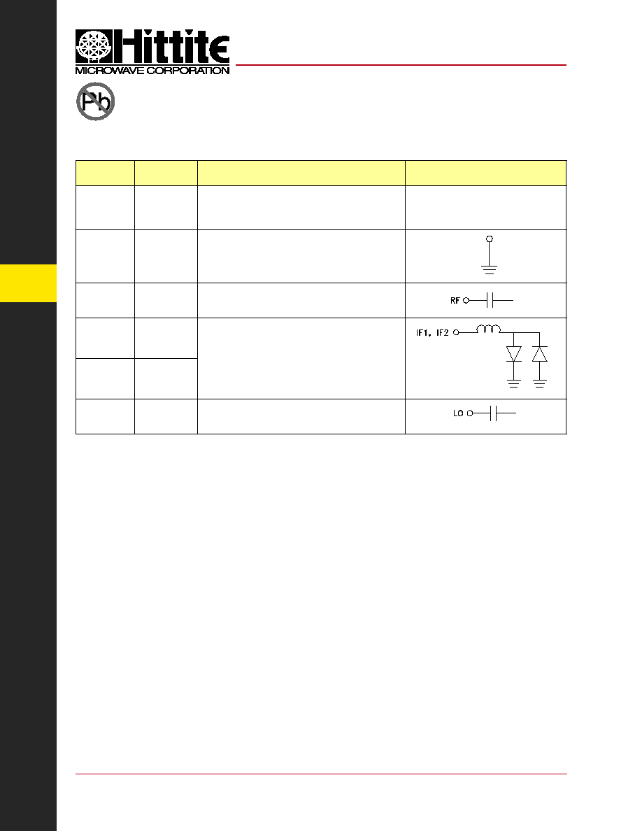
Pin
Number
Function
Description
Interface Schematic
1, 2, 6-8,
10, 13,
17-24
N/C
No connection required. These pins may be connected
to RF/DC ground without affecting performance.
3, 5, 12,
14, 16
GND
These pins and package bottom must be connected
to RF/DC ground.
4
RF
RF Port. This pin is AC coupled and matched to
50 Ohms from 8.5 to 13.5 GHz.
9
IF1
IF Port. This pin is DC coupled. For applications
not requiring operation to DC, this port should be
DC blocked externally using a series capacitor whose
value has been chosen to pass the necessary IF
frequency range. For operation to DC, this pin must not
source/sink more than 3mA of current or part non-func-
tion and possible part failure will result.
11
IF2
15
LO
LO Port. This pin is AC coupled and matched to
50 Ohms from 8.5 to 13.5 GHz.
Pin Descriptions
HMC521LC4
GaAs MMIC I/Q MIXER
8.5 - 13.5 GHz
v00.0105