VC
O
S
& P
L
Os - SM
T
11
11 - 188
For price, delivery, and to place orders, please contact Hittite Microwave Corporation:
20 Alpha Road, Chelmsford, MA 01824 Phone: 978-250-3343 Fax: 978-250-3373
Order On-line at www.hittite.com
HMC534LP5
/
534LP5E
MMIC VCO w/ HALF FREQUENCY OUTPUT
& DIVIDE-BY-4, 10.6 - 11.8 GHz
v00.0606
General Description
Features
Functional Diagram
The HMC534LP5 & HMC534LP5E are GaAs InGaP
Heterojunction Bipolar Transistor (HBT) MMIC VCOs.
The HMC534LP5 & HMC534LP5E integrate resona-
tors, negative resistance devices, varactor diodes
and feature half frequency and divide-by-4 outputs.
The VCO's phase noise performance is excellent over
temperature, shock, and process due to the oscillator's
monolithic structure. Power output is +11 dBm typical
from a +5V supply voltage. The prescaler and RF/2
functions can be disabled to conserve current if not
required. The voltage controlled oscillator is packaged
in a leadless QFN 5x5 mm surface mount package,
and requires no external matching components.
Dual Output: Fo = 10.6 - 11.8 GHz
Fo/2 = 5.3 - 5.9 GHz
Pout: +11 dBm
Phase Noise: -110 dBc/Hz @100 kHz Typ.
No External Resonator Needed
QFN Leadless SMT Package, 25 mm
2
Typical Applications
Low noise MMIC VCO w/Half Frequency, Divide-by-4
Outputs for:
� Point to Point/Multipoint Radio
� Test Equipment & Industrial Controls
� SATCOM
� Military End-Use
Electrical Specifications,
T
A
= +25� C, Vcc (Dig), Vcc (Amp), Vcc (RF) = +5V
Parameter
Min.
Typ.
Max.
Units
Frequency Range
Fo
Fo/2
10.6 - 11.8
5.3 - 5.9
GHz
GHz
Power Output
RFOUT
RFOUT/2
RFOUT/4
+9
+8
-9
+14
+14
-3
dBm
dBm
dBm
SSB Phase Noise @ 100 kHz Offset,
Vtune= +5V @ RFOUT
-110
dBc/Hz
Tune Voltage
Vtune
2
12
V
Supply Current
Icc(Dig) + Icc(Amp) + Icc(RF)
310
350
380
mA
Tune Port Leakage Current (Vtune= 12V)
10
A
Output Return Loss
2
dB
Harmonics/Subharmonics
1/2
3/2
2nd
3rd
27
23
17
31
dBc
dBc
dBc
dBc
Pulling (into a 2.0:1 VSWR)
2
MHz pp
Pushing @ Vtune= 5V
20
MHz/V
Frequency Drift Rate
1.3
MHz/�C

VC
O
S
& P
L
Os - SM
T
11
11 - 189
For price, delivery, and to place orders, please contact Hittite Microwave Corporation:
20 Alpha Road, Chelmsford, MA 01824 Phone: 978-250-3343 Fax: 978-250-3373
Order On-line at www.hittite.com
Frequency vs. Tuning Voltage, Vcc = +5V
Sensitivity vs. Tuning Voltage, Vcc = +5V
SSB Phase Noise vs. Tuning Voltage
Frequency vs. Tuning Voltage, T= 25�C
Output Power
vs. Tuning Voltage, Vcc = +5V
SSB Phase Noise @ Vtune = +5V
8.8
9.2
9.6
10
10.4
10.8
11.2
11.6
12
12.4
0
1
2
3
4
5
6
7
8
9
10
11
12
13
+25C
+85C
-40C
OUTPUT FREQUENCY (GHz)
TUNING VOLTAGE (VOLTS)
HMC534LP5
/
534LP5E
0
100
200
300
400
500
600
700
0
1
2
3
4
5
6
7
8
9
10
11
12
13
+25C
+85C
-40C
SENSITIVITY (MHz/V)
TUNING VOLTAGE (VOLTS)
8.8
9.2
9.6
10
10.4
10.8
11.2
11.6
12
12.4
0
1
2
3
4
5
6
7
8
9
10
11
12
13
4.75V
5.00V
5.25V
OUTPUT FREQUENCY (GHz)
TUNING VOLTAGE (VOLTS)
0
2
4
6
8
10
12
14
16
0
1
2
3
4
5
6
7
8
9
10
11
12
13
+25C
+85C
-40C
OUTPUT POWER (dBm)
TUNING VOLTAGE (VOLTS)
MMIC VCO w/ HALF FREQUENCY OUTPUT
& DIVIDE-BY-4, 10.6 - 11.8 GHz
v00.0606
-120
-115
-110
-105
-100
-95
-90
-85
-80
-75
-70
0
1
2
3
4
5
6
7
8
9
10 11 12 13
10kHz OFFSET
100kHz OFFSET
SSB PHASE NOISE (dBc/Hz)
TUNING VOLTAGE (VOLTS)
-180
-160
-140
-120
-100
-80
-60
-40
-20
0
10
3
10
4
10
5
10
6
10
7
+25C
+85C
-40C
SSB PHASE NOISE (dBc/Hz)
OFFSET FREQUENCY (Hz)

VC
O
S
& P
L
Os - SM
T
11
11 - 190
For price, delivery, and to place orders, please contact Hittite Microwave Corporation:
20 Alpha Road, Chelmsford, MA 01824 Phone: 978-250-3343 Fax: 978-250-3373
Order On-line at www.hittite.com
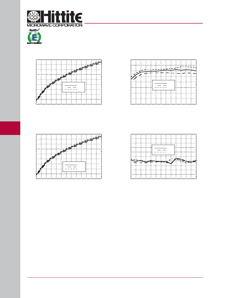
RFOUT/2 Frequency
vs. Tuning Voltage, Vcc = +5V
RFOUT/2 Output Power
vs. Tuning Voltage, Vcc = +5V
Divide-by-4 Frequency
vs. Tuning Voltage, Vcc = +5V
Divide-by-4 Output Power
vs. Tuning Voltage, Vcc = +5V
-10
-9
-8
-7
-6
-5
-4
-3
-2
-1
0
0
1
2
3
4
5
6
7
8
9
10
11
12
13
+25C
+85C
-40C
OUTPUT POWER (dBm)
TUNING VOLTAGE (VOLTS)
2.2
2.3
2.4
2.5
2.6
2.7
2.8
2.9
3
3.1
0
1
2
3
4
5
6
7
8
9
10
11
12
13
+25C
+85C
-40C
OUTPUT FREQUENCY (GHz)
TUNING VOLTAGE (VOLTS)
0
2
4
6
8
10
12
14
16
0
1
2
3
4
5
6
7
8
9
10
11
12
13
+25C
+85C
-40C
OUTPUT POWER (dBm)
TUNING VOLTAGE (VOLTS)
4.4
4.6
4.8
5
5.2
5.4
5.6
5.8
6
6.2
0
1
2
3
4
5
6
7
8
9
10
11
12
13
+25C
+85C
-40C
OUTPUT FREQUENCY (GHz)
TUNING VOLTAGE (VOLTS)
v00.0606
HMC534LP5
/
534LP5E
MMIC VCO w/ HALF FREQUENCY OUTPUT
& DIVIDE-BY-4, 10.6 - 11.8 GHz

VC
O
S
& P
L
Os - SM
T
11
11 - 191
For price, delivery, and to place orders, please contact Hittite Microwave Corporation:
20 Alpha Road, Chelmsford, MA 01824 Phone: 978-250-3343 Fax: 978-250-3373
Order On-line at www.hittite.com
Absolute Maximum Ratings
Outline Drawing
Vcc(Dig), Vcc(Amp), Vcc(RF)
+5.5 Vdc
Vtune
0 to +15V
Junction Temperature
135 �C
Continuous Pdiss (T=85 �C)
(derate 43.5 mW/C above 85 �C
2.17 W
Thermal Resistance
(junction to ground paddle)
23 �C/W
Storage Temperature
-65 to +150 �C
Operating Temperature
-40 to +85 �C
ESD Sensitivity (HBM)
Class 1A
Typical Supply Current vs. Vcc
Note: VCO will operate over full voltage range shown above.
Vcc (V)
Icc (mA)
4.75
320
5.00
350
5.25
380
ELECTROSTATIC SENSITIVE DEVICE
OBSERVE HANDLING PRECAUTIONS
NOTES:
1. LEADFRAME MATERIAL: COPPER ALLOY
2. DIMENSIONS ARE IN INCHES [MILLIMETERS]
3. LEAD SPACING TOLERANCE IS NON-CUMULATIVE.
4. PAD BURR LENGTH SHALL BE 0.15mm MAXIMUM.
PAD BURR HEIGHT SHALL BE 0.05mm MAXIMUM.
5. PACKAGE WARP SHALL NOT EXCEED 0.05mm.
6. ALL GROUND LEADS AND GROUND PADDLE MUST BE
SOLDERED TO PCB RF GROUND.
7. REFER TO HITTITE APPLICATION NOTE FOR SUGGESTED
LAND PATTERN.
Part Number
Package Body Material
Lead Finish
MSL Rating
Package Marking
[3]
HMC534LP5
Low Stress Injection Molded Plastic
Sn/Pb Solder
MSL1
[1]
H534
XXXX
HMC534LP5E
RoHS-compliant Low Stress Injection Molded Plastic
100% matte Sn
MSL1
[2]
H534
XXXX
[1] Max peak refl ow temperature of 235 �C
[2] Max peak refl ow temperature of 260 �C
[3] 4-Digit lot number XXXX
Package Information
v00.0606
HMC534LP5
/
534LP5E
MMIC VCO w/ HALF FREQUENCY OUTPUT
& DIVIDE-BY-4, 10.6 - 11.8 GHz

VC
O
S
& P
L
Os - SM
T
11
11 - 192
For price, delivery, and to place orders, please contact Hittite Microwave Corporation:
20 Alpha Road, Chelmsford, MA 01824 Phone: 978-250-3343 Fax: 978-250-3373
Order On-line at www.hittite.com
Pin Number
Function
Description
Interface Schematic
1-3, 5, 8-11,
13-18, 20,
22-28, 30-32
N/C
No Connection. These pins may be connected to RF/
DC ground. Performance will not be affected.
4
RFOUT/4
Divide-by-4 output.
DC block required
6
Vcc (Dig)
Supply voltage for prescaler. If prescaler is not
required, this pin may be left open to conserve
approximately 65 mA of current.
7
Vcc (Amp)
Supply voltage, for RFOUT/2 output. If RFOUT/2
is not required. This pin may be left open to
conserve approximately 30 mA of current.
12
RFOUT/2
Half frequency output (AC coupled).
19
RF OUT
RF output (AC coupled).
21
Vcc (RF)
Supply Voltage, +5V
29
VTUNE
Control voltage and modulation input. Modulation
bandwidth dependent on drive source impedance. See
"Determining the FM Bandwidth of a Wideband Varac-
tor Tuned VCO" application note.
GND
Package bottom has an exposed metal paddle that
must be connected to RF/DC ground.
Pin Descriptions
v00.0606
HMC534LP5
/
534LP5E
MMIC VCO w/ HALF FREQUENCY OUTPUT
& DIVIDE-BY-4, 10.6 - 11.8 GHz


