 | –≠–ª–µ–∫—Ç—Ä–æ–Ω–Ω—ã–π –∫–æ–º–ø–æ–Ω–µ–Ω—Ç: HMC574MS8 | –°–∫–∞—á–∞—Ç—å:  PDF PDF  ZIP ZIP |
14
S
W
I
T
C
H
E
S
- SM
T
14 - 324
For price, delivery, and to place orders, please contact Hittite Microwave Corporation:
20 Alpha Road, Chelmsford, MA 01824 Phone: 978-250-3343 Fax: 978-250-3373
Order On-line at www.hittite.com
HMC574MS8
/
574MS8E
GaAs MMIC 5 WATT T/R SWITCH
DC - 3 GHz
v00.0805
General Description
Features
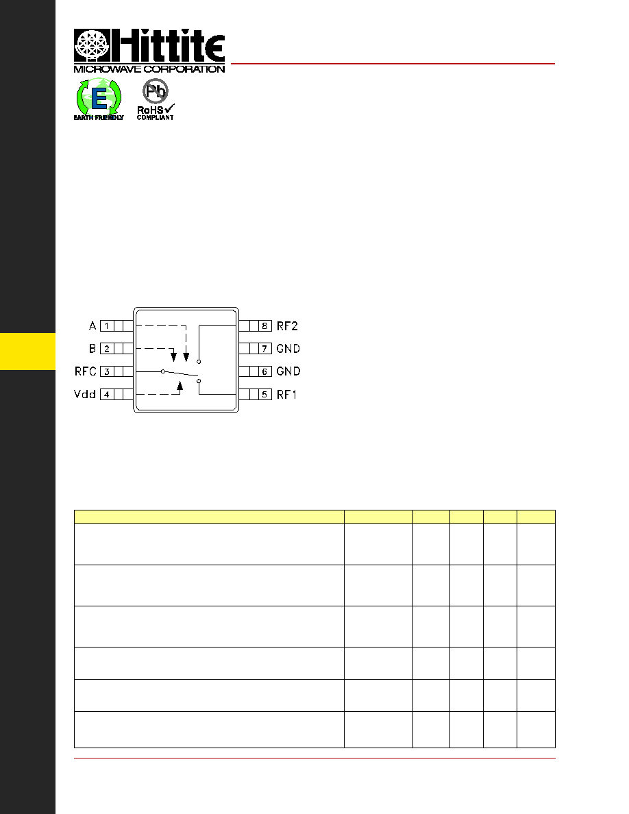
Functional Diagram
Low Insertion Loss: 0.3 dB
High Third Order Intercept: +65 dBm
Isolation: 30 dB
Single Positive Supply: +3 to +10V
SMT Package: MSOP8
Electrical Specifications,
T
A
= +25∞ C, Vctl = 0/+5 Vdc, Vdd = +5 Vdc (Unless Otherwise Stated), 50 Ohm System
Typical Applications
The HMC574MS8 / HMC574MS8E is ideal for:
∑ Cellular/3G Infrastructure
∑ Private Mobile Radio Handsets
∑ WLAN, WiMAX & WiBro
∑ Automotive Telematics
∑ Test Equipment
The HMC574MS8 & HMC574MS8E are low-cost
SPDT switches in 8-lead MSOP packages for use in
transmit/receive applications which require very low
distortion at high incident power levels. The device
can control signals from DC to 3.0 GHz and is es-
pecially suited for Cellular/3G infrastructure, WiMAX
and WiBro applications with only 0.3 dB typical
insertion loss. The design provides 5 watt power
handling performance and +65 dBm third order
interceptat +8 Volt bias. RF1 and RF2 are refl ective
shorts when "Off". Control inputs A & B are compatible
with CMOS and some TTL logic families. These
products are form, fi t and function replacements for
HMC174MS8 & HMC174MS8E while offering superior
electrical performance.
Parameter
Frequency
Min.
Typ.
Max.
Units
Insertion Loss
DC - 1.0 GHz
DC - 2.0 GHz
DC - 2.5 GHz
DC - 3.0 GHz
0.25
0.3
0.4
0.5
0.5
0.6
0.7
0.8
dB
dB
dB
dB
Isolation
DC - 1.0 GHz
DC - 2.0 GHz
DC - 2.5 GHz
DC - 3.0 GHz
26
24
21
16
30
28
25
20
dB
dB
dB
dB
Return Loss
DC - 1.0 GHz
DC - 2.0 GHz
DC - 2.5 GHz
DC - 3.0 GHz
35
25
18
16
dB
dB
dB
dB
Input Power for 1dB Compression
Vctl = 0/+3V
Vctl = 0/+5V
Vctl = 0/+8V
0.5 - 3.0 GHz
33
35
37
36
38
39
dBm
dBm
dBm
Input Third Order Intercept
(Two-tone Input Power = +27 dBm Each Tone)
Vctl = 0/+3V
Vctl = 0/+5V
Vctl = 0/+8V
0.5 - 3.0 GHz
55
63
65
dBm
dBm
dBm
Switching Characteristics
DC - 3.0 GHz
tRISE, tFALL (10/90% RF)
tON, tOFF (50% CTL to 10/90% RF)
80
120
ns
ns

14
S
W
I
T
C
H
E
S
- SM
T
14 - 325
For price, delivery, and to place orders, please contact Hittite Microwave Corporation:
20 Alpha Road, Chelmsford, MA 01824 Phone: 978-250-3343 Fax: 978-250-3373
Order On-line at www.hittite.com
Insertion Loss
Isolation Between RFC & RF1/RF2
Return Loss
HMC574MS8
/
574MS8E
v00.0805
-2
-1.5
-1
-0.5
0
0
1
2
3
4
+25C
+85C
-40C
INSERTION LOSS (dB)
FREQUENCY (GHz)
-40
-30
-20
-10
0
0
1
2
3
4
+25C
+85C
-40C
RETURN LOSS (dB)
FREQUENCY (GHz)
-40
-30
-20
-10
0
0
1
2
3
4
+25C
+85C
-40C
ISOLATION (dB)
FREQUENCY (GHz)
Input P1dB vs. Vdd
RF1 to RF2 Isolation
-50
-40
-30
-20
-10
0
0
1
2
3
4
RF1 ON
RF2 ON
ISOLATION (dB)
FREQUENCY (GHz)
26
28
30
32
34
36
38
40
42
0
1
2
3
4
+8V
+5V
+3V
INPUT P1dB (dBm)
FREQUENCY (GHz)
Input P0.1dB vs. Vdd
26
28
30
32
34
36
38
40
42
0
1
2
3
4
+8V
+5V
+3V
INPUT P0.1dB (dBm)
FREQUENCY (GHz)
GaAs MMIC 5 WATT T/R SWITCH
DC - 3 GHz

14
S
W
I
T
C
H
E
S
- SM
T
14 - 326
For price, delivery, and to place orders, please contact Hittite Microwave Corporation:
20 Alpha Road, Chelmsford, MA 01824 Phone: 978-250-3343 Fax: 978-250-3373
Order On-line at www.hittite.com
HMC574MS8
/
574MS8E
v00.0805
Input IP3 vs. Input Power @ 900 MHz
Input IP3 vs. Input Power @ 1900 MHz
2nd & 3rd Harmonics @ 900 MHz
Vdd = +8 Volts
45
50
55
60
65
70
27
28
29
30
31
32
33
+10V
+8V
+5V
INPUT IP3 (dBm)
TWO TONE INPUT POWER (dBm) (EACH TONE)
-1
-0.9
-0.8
-0.7
-0.6
-0.5
-0.4
-0.3
-0.2
-0.1
0
-100
-90
-80
-70
-60
-50
-40
-30
-20
-10
0
28
29
30
31
32
33
34
35
36
37
38
39
40
F2
F3
INSERTION LOSS (dB)
HARMONI
CS
(dB
c
)
INPUT POWER (dBm)
45
50
55
60
65
70
27
28
29
30
31
32
33
+10V
+8V
+5V
INPUT IP3 (dBm)
TWO TONE INPUT POWER (dBm) (EACH TONE)
2nd & 3rd Harmonics @ 900 MHz
Vdd = +5 Volts
2nd & 3rd Harmonics @ 900 MHz
Vdd = +3 Volts
-1
-0.9
-0.8
-0.7
-0.6
-0.5
-0.4
-0.3
-0.2
-0.1
0
-100
-90
-80
-70
-60
-50
-40
-30
-20
-10
0
24
25
26
27
28
29
30
31
32
33
34
35
36
F2
F3
INSERTION LOSS (dB)
HARMONI
CS
(dB
c
)
INPUT POWER (dBm)
-1
-0.9
-0.8
-0.7
-0.6
-0.5
-0.4
-0.3
-0.2
-0.1
0
-100
-90
-80
-70
-60
-50
-40
-30
-20
-10
0
26
27
28
29
30
31
32
33
34
35
36
37
38
F2
F3
INSERTION LOSS (dB)
HARMONI
CS
(dB
c
)
INPUT POWER (dBm)
Input Third Order Intercept
40
45
50
55
60
65
70
0
1
2
3
4
+10V
+8V
+5V
+3V
INPUT IP3 (dBm)
FREQUENCY (GHz)
GaAs MMIC 5 WATT T/R SWITCH
DC - 3 GHz

14
S
W
I
T
C
H
E
S
- SM
T
14 - 327
For price, delivery, and to place orders, please contact Hittite Microwave Corporation:
20 Alpha Road, Chelmsford, MA 01824 Phone: 978-250-3343 Fax: 978-250-3373
Order On-line at www.hittite.com
HMC574MS8
/
574MS8E
v00.0805
Absolute Maximum Ratings
Max. Input Power
V
dd
= 0/+8V
0.5 - 2.5 GHz
39 dBm
Bias Voltage Range (Vdd)
-0.2 to +12 Vdc
Control Voltage Range (A & B)
-0.2 to +Vdd Vdc
Hot Switching Power Level
V
dd
= +8V
39 dBm
Channel Temperature
150 ∞C
Continuous Pdiss ( T= + 85 ∞C)
(derate 10 mW/∞C above 85 ∞C)
0.65W
Thermal Resistance
100 ∞C/W
Storage Temperature
-65 to +150 ∞C
Operating Temperature
-40 to +85 ∞C
ESD Sensitivity (HBM)
Class 1A
DC Blocks are required at ports RFC, RF1 and RF2
ELECTROSTATIC SENSITIVE DEVICE
OBSERVE HANDLING PRECAUTIONS
Truth Table
Control Input (Vctl)
Signal Path State
A
B
RFC to RF1
RFC to RF2
High
Low
Off
On
Low
High
On
Off
Control Voltages
Bias Voltage & Current
Vdd (Vdc)
Typical Idd (A)
+3
2
+5
10
+8
40
State
Bias Condition
Low
0 to +0.2 Vdc @ 10 A Typical
High
Vdd ± 0.2 Vdc @ 10 A Typical
GaAs MMIC 5 WATT T/R SWITCH
DC - 3 GHz
Input P0.1dB vs. Vdd
Input P1dB vs. Vdd
20
25
30
35
40
0.01
0.1
1
+8V
+5V
+3V
INPUT P1dB (dBm)
FREQUENCY (GHz)
20
25
30
35
40
0.01
0.1
1
+8V
+5V
+3V
INPUT P0.1dB (dBm)
FREQUENCY (GHz)

14
S
W
I
T
C
H
E
S
- SM
T
14 - 328
For price, delivery, and to place orders, please contact Hittite Microwave Corporation:
20 Alpha Road, Chelmsford, MA 01824 Phone: 978-250-3343 Fax: 978-250-3373
Order On-line at www.hittite.com
HMC574MS8
/
574MS8E
v00.0805
Outline Drawing
NOTES:
1. LEADFRAME MATERIAL: COPPER ALLOY
2. DIMENSIONS ARE IN INCHES [MILLIMETERS]
3. DIMENSION DOES NOT INCLUDE MOLDFLASH OF 0.15mm PER SIDE.
4. DIMENSION DOES NOT INCLUDE MOLDFLASH OF 0.25mm PER SIDE.
5. ALL GROUND LEADS MUST BE SOLDERED TO PCB RF GROUND.
Part Number
Package Body Material
Lead Finish
MSL Rating
Package Marking
[3]
HMC574MS8
Low Stress Injection Molded Plastic
Sn/Pb Solder
MSL1
[1]
H574
XXXX
HMC574MS8E
RoHS-compliant Low Stress Injection Molded Plastic
100% matte Sn
MSL1
[2]
H574
XXXX
[1] Max peak refl ow temperature of 235 ∞C
[2] Max peak refl ow temperature of 260 ∞C
[3] 4-Digit lot number XXXX
Package Information
GaAs MMIC 5 WATT T/R SWITCH
DC - 3 GHz