7_freqmultiplier_smt_section.indd
F
R
E
Q
U
E
NC
Y MU
L
T
I
P
L
I
E
R
S - SM
T
7
7 - 100
For price, delivery, and to place orders, please contact Hittite Microwave Corporation:
20 Alpha Road, Chelmsford, MA 01824 Phone: 978-250-3343 Fax: 978-250-3373
Order On-line at www.hittite.com
HMC578LC3B
SMT GaAs MMIC x2 ACTIVE FREQUENCY
MULTIPLIER, 24 - 33 GHz OUTPUT
v00.0506
General Description
Features
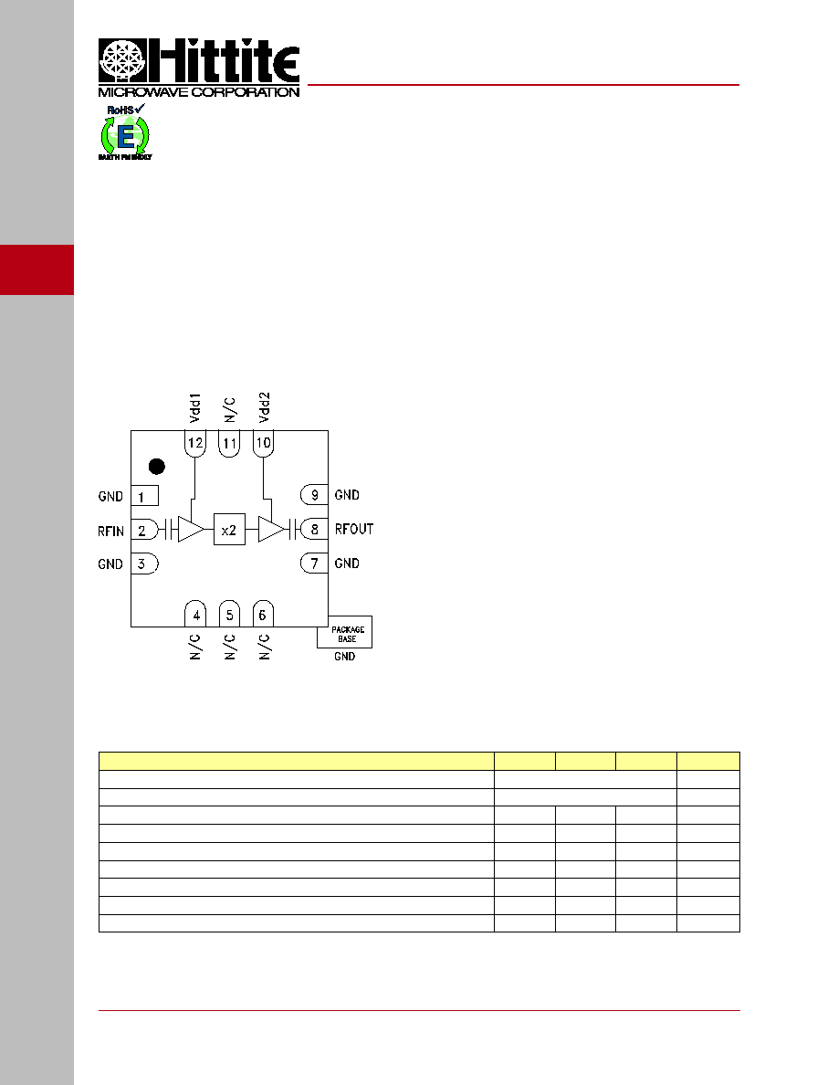
Functional Diagram
Electrical Specifications,
T
A
= +25° C, Vdd1, Vdd2 = +5V, 3 dBm Drive Level
Typical Applications
The HMC578LC3B is suitable for:
· Clock Generation Applications:
SONET OC-192 & SDH STM-64
· Point-to-Point & VSAT Radios
· Test Instrumentation
· Military & Space
The HMC578LC3B is a x2 active broadband frequ-
ency multiplier utilizing GaAs PHEMT technology in a
leadless RoHS compliant SMT package. When driven
by a +3 dBm signal, the multiplier provides +15 dBm
typical output power from 24 to 33 GHz. The Fo and
3Fo isolations are >20 dBc and >30 dBc respectively
at 28 GHz. The HMC578LC3B is ideal for use in LO
multiplier chains for Pt to Pt & VSAT Radios yielding
reduced parts count vs. traditional approaches. The
low additive SSB Phase Noise of -129 dBc/Hz at
100 kHz offset helps maintain good system noise
performance. The RoHS packaged HMC578LC3B
eliminates the need for wire bonding, and allows the
use of surface mount manufacturing techniques.
High Output Power: +15 dBm
Low Input Power Drive: 0 to +6 dBm
Fo Isolation: >20 dBc @ Fout= 28 GHz
100 KHz SSB Phase Noise: -132 dBc/Hz
Single Supply: +5V@ 81 mA
RoHS Compliant 3x3 mm SMT Package
Parameter
Min.
Typ. Max.
Units
Frequency Range, Input
12 - 16.5
GHz
Frequency Range, Output
24 - 33
GHz
Output Power
10
15
dBm
Fo Isolation (with respect to output level)
20
dBc
3Fo Isolation (with respect to output level)
30
dBc
Input Return Loss
10
dB
Output Return Loss
12
dB
SSB Phase Noise (100 kHz Offset)
-132
dBc/Hz
Supply Current (Idd1 & Idd2)
81
mA
F
R
E
Q
U
E
NC
Y MU
L
T
I
P
L
I
E
R
S - SM
T
7
7 - 101
For price, delivery, and to place orders, please contact Hittite Microwave Corporation:
20 Alpha Road, Chelmsford, MA 01824 Phone: 978-250-3343 Fax: 978-250-3373
Order On-line at www.hittite.com
HMC578LC3B
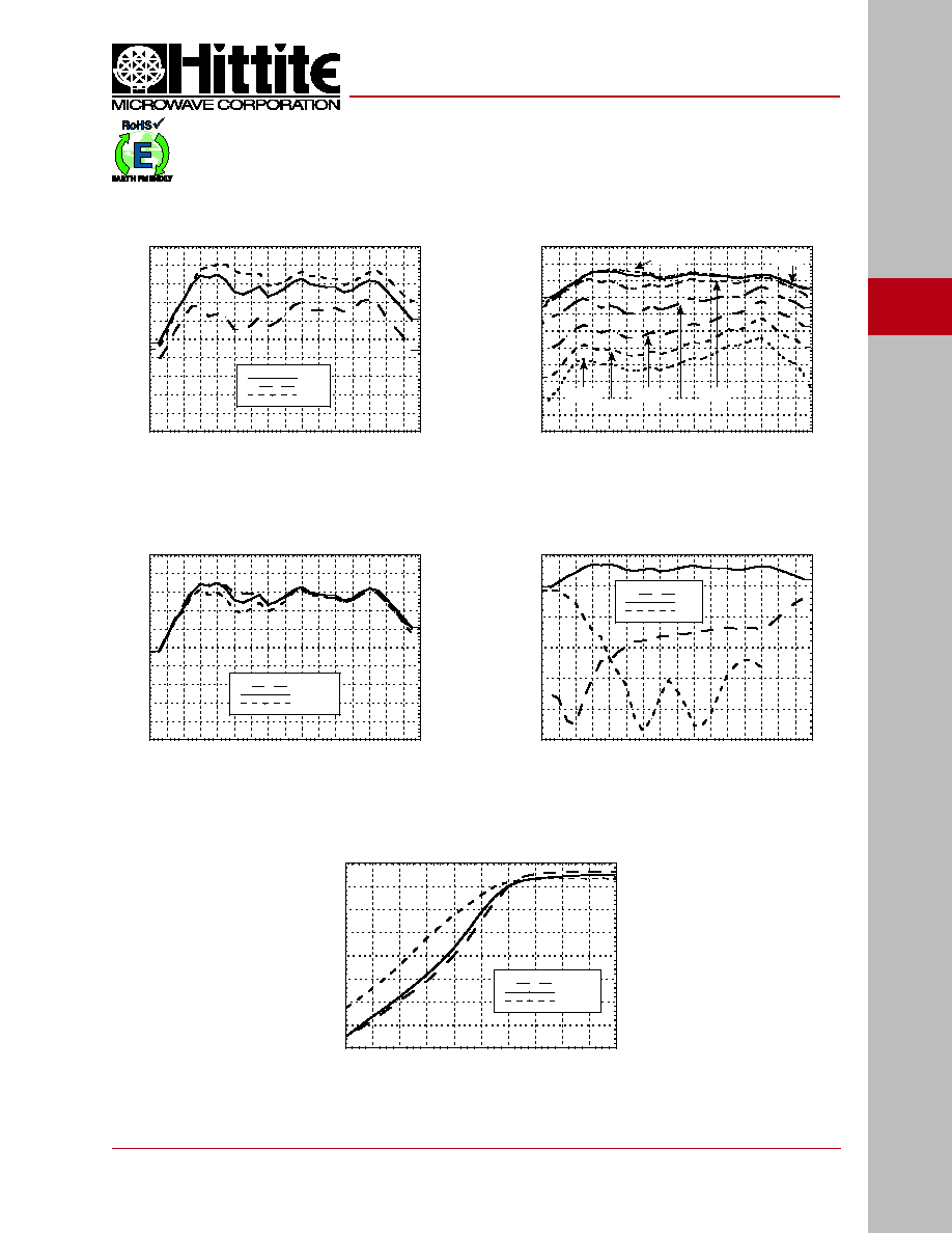
Output Power vs.
Temperature @ 3 dBm Drive Level
Output Power vs.
Supply Voltage @ 3 dBm Drive Level
Output Power vs. Drive Level
v00.0506
SMT GaAs MMIC x2 ACTIVE FREQUENCY
MULTIPLIER, 24 - 33 GHz OUTPUT
Output Power vs. Input Power
Isolation @ 3 dBm Drive Level
0
2
4
6
8
10
12
14
16
18
20
20 21 22 23 24 25 26 27 28 29 30 31 32 33 34 35 36
+25C
+85C
-40C
OUTPUT POWER (dBm)
OUTPUT FREQUENCY (GHz)
-40
-30
-20
-10
0
10
20
20 21 22 23 24 25 26 27 28 29 30 31 32 33 34 35 36
Fo
2Fo
3Fo
OUTPUT POWER (dBm)
OUTPUT FREQUENCY (GHz)
-20
-15
-10
-5
0
5
10
15
20
-10
-8
-6
-4
-2
0
2
4
6
8
10
24GHZ
28.5GHz
33GHz
OUTPUT POWER (dBm)
INPUT POWER (dBm)
0
2
4
6
8
10
12
14
16
18
20
20 21 22 23 24 25 26 27 28 29 30 31 32 33 34 35 36
Vdd=4.5V
Vdd=5.0V
Vdd=5.5V
OUTPUT POWER (dBm)
OUTPUT FREQUENCY (GHz)
-30
-25
-20
-15
-10
-5
0
5
10
15
20
25
20 21 22 23 24 25 26 27 28 29 30 31 32 33 34 35 36
OUTPUT POWER (dBm)
OUTPUT FREQUENCY (GHz)
-4 dBm
-6 dBm
-2 dBm
0 dBm
2 dBm
4 dBm
6 dBm
F
R
E
Q
U
E
NC
Y MU
L
T
I
P
L
I
E
R
S - SM
T
7
7 - 102
For price, delivery, and to place orders, please contact Hittite Microwave Corporation:
20 Alpha Road, Chelmsford, MA 01824 Phone: 978-250-3343 Fax: 978-250-3373
Order On-line at www.hittite.com
Input Return Loss vs. Temperature
Output Return Loss vs. Temperature
HMC578LC3B
v00.0506
SMT GaAs MMIC x2 ACTIVE FREQUENCY
MULTIPLIER, 24 - 33 GHz OUTPUT
-20
-18
-16
-14
-12
-10
-8
-6
-4
-2
0
20 21 22 23 24 25 26 27 28 29 30 31 32 33 34 35 36
+25C
+85C
-40C
OUTPUT RETURN LOSS (dB)
FREQUENCY (GHz)
-20
-15
-10
-5
0
10
11
12
13
14
15
16
17
18
+25C
+85C
-40C
INPUT RETURN LOSS (dB)
FREQUENCY (GHz)
F
R
E
Q
U
E
NC
Y MU
L
T
I
P
L
I
E
R
S - SM
T
7
7 - 103
For price, delivery, and to place orders, please contact Hittite Microwave Corporation:
20 Alpha Road, Chelmsford, MA 01824 Phone: 978-250-3343 Fax: 978-250-3373
Order On-line at www.hittite.com
Absolute Maximum Ratings
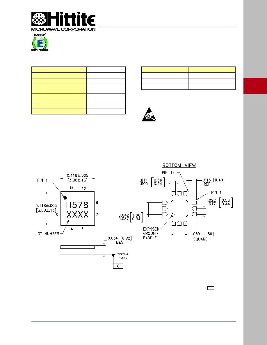
Outline Drawing
RF Input (Vdd = +5V)
+13 dBm
Supply Voltage (Vdd)
+6.0 Vdc
Channel Temperature
175 °C
Continuous Pdiss (T= 85 °C)
(derate 7.4 mW/°C above 85 °C)
670 mW
Thermal Resistance
(channel to ground paddle)
135 °C/W
Storage Temperature
-65 to +150 °C
Operating Temperature
-40 to +85 °C
Typical Supply Current vs. Vdd
Vdd (Vdc)
Idd (mA)
4.5
81
5.0
81
5.5
81
Note:
Multiplier will operate over full voltage range shown above.
ELECTROSTATIC SENSITIVE DEVICE
OBSERVE HANDLING PRECAUTIONS
NOTES:
1. PACKAGE BODY MATERIAL: ALUMINA
2. LEAD AND GROUND PADDLE PLATING: 30-80 MICROINCHES GOLD OVER
50 MICROINCHES MINIMUM NICKEL.
3. DIMENSIONS ARE IN INCHES [MILLIMETERS].
4. LEAD SPACING TOLERANCE IS NON-CUMULATIVE
5. PACKAGE WARP SHALL NOT EXCEED 0.05mm DATUM -C-
6. ALL GROUND LEADS AND GROUND PADDLE MUST BE SOLDERED
TO PCB RF GROUND.
7. CLASSIFIED AS MOISTURE SENSITIVITY LEVEL (MSL) 1.
HMC578LC3B
v00.0506
SMT GaAs MMIC x2 ACTIVE FREQUENCY
MULTIPLIER, 24 - 33 GHz OUTPUT

F
R
E
Q
U
E
NC
Y MU
L
T
I
P
L
I
E
R
S - SM
T
7
7 - 104
For price, delivery, and to place orders, please contact Hittite Microwave Corporation:
20 Alpha Road, Chelmsford, MA 01824 Phone: 978-250-3343 Fax: 978-250-3373
Order On-line at www.hittite.com
Pin Number
Function
Description
Interface Schematic
1, 3, 7, 9
GND
Package bottom must also be connected
to RF/DC ground.
2
RFIN
Pin is AC coupled and matched to 50 Ohms
from 12 - 16.5 GHz.
4 - 6, 11
N/C
These pins are internally not connected; however,
this product was specifi ed with these pins connected
to RF/ DC ground.
8
RFOUT
Pin is AC coupled and matched to 50 Ohms
from 24 - 33 GHz.
10, 12
Vdd2, Vdd1
Supply voltage 5V ± 0.5V. External bypass capacitors
of 100 pF, 1,000 pF and 2.2 F are required.
Pin Description
Application Circuit
Component
Value
C1, C2
100 pF
C3, C4
1,000 pF
C5, C6
2.2 F
HMC578LC3B
v00.0506
SMT GaAs MMIC x2 ACTIVE FREQUENCY
MULTIPLIER, 24 - 33 GHz OUTPUT