V
C
Os & P
L
Os - SM
T
9
9 - 166
For price, delivery, and to place orders, please contact Hittite Microwave Corporation:
20 Alpha Road, Chelmsford, MA 01824 Phone: 978-250-3343 Fax: 978-250-3373
Order On-line at www.hittite.com
WIDEBAND MMIC VCO w/ BUFFER
AMPLIFIER, 4.0 - 8.0 GHz
v00.0206
General Description
Features
Functional Diagram
The HMC586LC4B is a wideband GaAs InGaP
Voltage Controlled Oscillator which incorporates the
resonator, negative resistance device, and varactor
diode. Output power and phase noise performance
are excellent over temperature due to the oscillator's
monolithic construction. The Vtune port accepts
an analog tuning voltage from 0 to +18V. The
HMC586LC4B VCO operates from a single +5V sup-
ply, consumes only 55 mA of current, and is housed in
a RoHS compliant SMT package. This wideband VCO
uniquely combines the attributes of ultra small size,
low phase noise, low power consumption, and wide
tuning range.
Wide Tuning Bandwidth
Pout: +5 dBm
Low SSB Phase Noise: -100 dBc/Hz @100 kHz
No External Resonator Needed
Single Positive Supply: +5V @ 55 mA
RoHS Compliant 4 x 4 mm SMT Package
Typical Applications
Low Noise wideband MMIC VCO is ideal for:
� Industrial/Medical Equipment
� Test & Measurement Equipment
� Military Radar, EW & ECM
Electrical Specifications,
T
A
= +25� C, Vcc = +5V
Parameter
Min.
Typ.
Max.
Units
Frequency Range
4.0 - 8.0
GHz
Power Output
2
5
dBm
SSB Phase Noise @ 100 kHz Offset
-100
dBc/Hz
SSB Phase Noise @ 10 kHz Offset
-75
dBc/Hz
Tune Voltage (Vtune)
0
18
V
Supply Current (Icc) (Vcc = +5.0V)
40
75
mA
Tune Port Leakage Current (Vtune = +15V)
10
A
Output Return Loss
7
dB
2nd Harmonic
-14
dBc
Pulling (into a 2.0:1 VSWR)
4
MHz pp
Pushing @ Vtune= +5V
40
MHz/V
Frequency Drift Rate
0.8
MHz/�C
HMC586LC4B

V
C
Os & P
L
Os - SM
T
9
9 - 167
For price, delivery, and to place orders, please contact Hittite Microwave Corporation:
20 Alpha Road, Chelmsford, MA 01824 Phone: 978-250-3343 Fax: 978-250-3373
Order On-line at www.hittite.com
Frequency vs. Tuning Voltage, Vcc = +5V
Sensitivity vs. Tuning Voltage, Vcc= +5V
Typical SSB Phase Noise @ Vtune= +5V
SSB Phase Noise vs. Tuning Voltage
Output Power vs.
Tuning Voltage, Vcc= +5V
HMC586LC4B
v00.0206
3
4
5
6
7
8
9
0
2
4
6
8
10
12
14
16
18
20
4.75 V
5.0 V
5.25 V
OUTPUT FREQUENCY (GHz)
TUNING VOLTAGE (VOLTS)
Frequency vs. Tuning Voltage, T = +25 C
WIDEBAND MMIC VCO w/ BUFFER
AMPLIFIER, 4.0 - 8.0 GHz
-4
-2
0
2
4
6
8
10
0
2
4
6
8
10
12
14
16
18
20
+25 C
+85 C
-40 C
OUTPUT POWER (dBm)
TUNING VOLTAGE (VOLTS)
0
100
200
300
400
500
600
0
2
4
6
8
10
12
14
16
18
20
+25 C
+85 C
-40 C
SENSITIVITY (MHz/VOLT)
TUNING VOLTAGE (VOLTS)
-120
-110
-100
-90
-80
-70
-60
-50
-40
-30
-20
-10
0
10
2
10
3
10
4
10
5
10
6
SSB PHASE NOISE (dBc/Hz)
OFFSET FREQUENCY (Hz)
-120
-110
-100
-90
-80
-70
-60
-50
-40
-30
-20
-10
0
0
2
4
6
8
10
12
14
16
18
20
10 kHz
100 kHz
SSB PHASE NOISE (dBc/Hz)
TUNING VOLTAGE (VOLTS)
3
4
5
6
7
8
9
0
2
4
6
8
10
12
14
16
18
20
+25 C
+85 C
-40 C
OUTPUT FREQUENCY (GHz)
TUNING VOLTAGE (VOLTS)

V
C
Os & P
L
Os - SM
T
9
9 - 168
For price, delivery, and to place orders, please contact Hittite Microwave Corporation:
20 Alpha Road, Chelmsford, MA 01824 Phone: 978-250-3343 Fax: 978-250-3373
Order On-line at www.hittite.com
Absolute Maximum Ratings
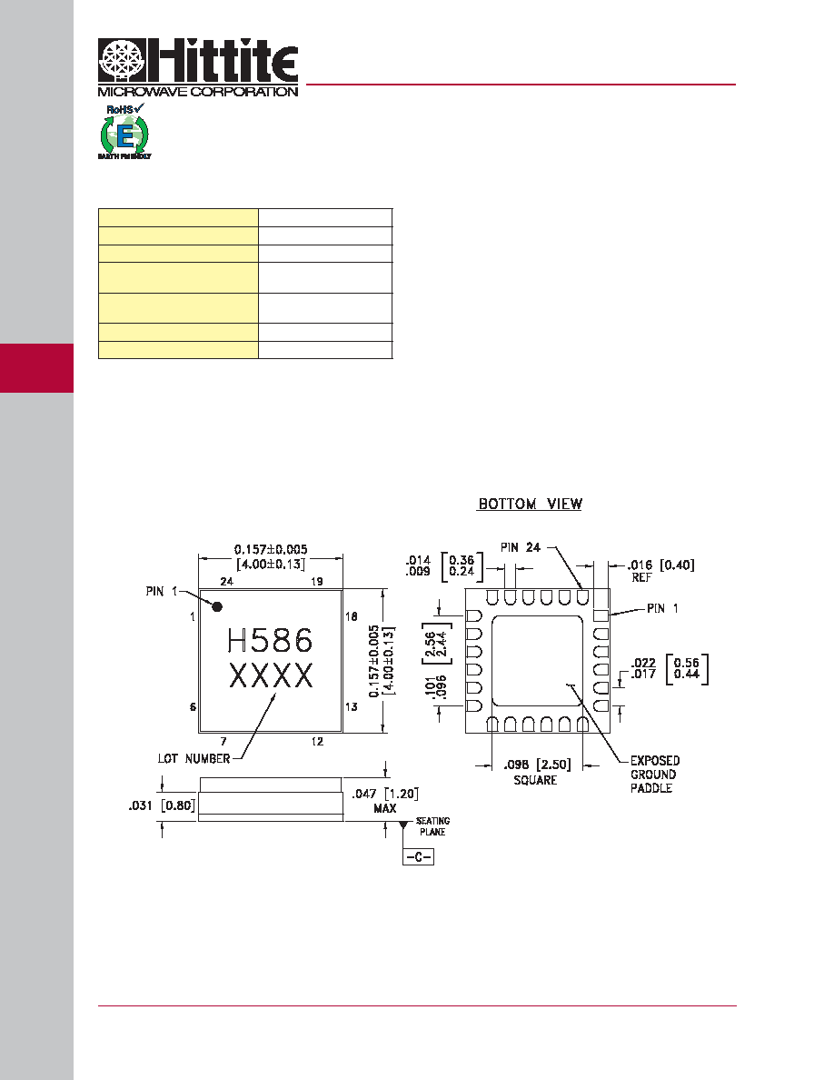
Outline Drawing
Vcc
+5.5 Vdc
Vtune
0 to +22V
Junction Temperature
135 �C
Continuous Pdiss (T = 85�C)
(derate 12.5 mW/�C above 85�C)
625 mW
Thermal Resistance
(junction to ground paddle)
80 �C/W
Storage Temperature
-65 to +150 �C
Operating Temperature
-40 to +85 �C
NOTES:
1. PACKAGE BODY MATERIAL: ALUMINA
2. LEAD AND GROUND PADDLE PLATING: GOLD FLASH OVER Ni.
3. DIMENSIONS ARE IN INCHES [MILLIMETERS].
4. LEAD SPACING TOLERANCE IS NON-CUMULATIVE.
5. PACKAGE WARP SHALL NOT EXCEED 0.05mm DATUM -C-
6. ALL GROUND LEADS AND GROUND PADDLE MUST BE SOLDERED
TO PCB RF GROUND.
HMC586LC4B
v00.0206
WIDEBAND MMIC VCO w/ BUFFER
AMPLIFIER, 4.0 - 8.0 GHz

V
C
Os & P
L
Os - SM
T
9
9 - 169
For price, delivery, and to place orders, please contact Hittite Microwave Corporation:
20 Alpha Road, Chelmsford, MA 01824 Phone: 978-250-3343 Fax: 978-250-3373
Order On-line at www.hittite.com
Pin Number
Function
Description
Interface Schematic
1 - 3, 5 - 11,
13, 17 - 24
N/C
No Connection. These pins may be connected to RF/DC
ground. Performance will not be affected.
4
Vtune
Control Voltage and Modulation Input. Modulation
bandwidth dependent on drive source impedance. See
"Determining the FM Bandwidth of a Wideband Varactor
Tuned VCO" application note.
12
Vcc
Supply Voltage Vcc= +5V
14, 16
GND
Package bottom has an exposed metal paddle that
must also be RF & DC grounded.
15
RFOUT
RF output (AC coupled)
Pin Descriptions
HMC586LC4B
v00.0206
WIDEBAND MMIC VCO w/ BUFFER
AMPLIFIER, 4.0 - 8.0 GHz

V
C
Os & P
L
Os - SM
T
9
9 - 170
For price, delivery, and to place orders, please contact Hittite Microwave Corporation:
20 Alpha Road, Chelmsford, MA 01824 Phone: 978-250-3343 Fax: 978-250-3373
Order On-line at www.hittite.com
The circuit board used in the fi nal application
should use RF circuit design techniques. Signal
lines should have 50 ohm impedance while the
package ground leads and exposed ground paddle
should be connected directly to the ground plane
similar to that shown. A suffi cient number of via
holes should be used to connect the top and bottom
ground planes. The evaluation circuit board shown
is available from Hittite upon request.
Evaluation PCB
List of Materials for Evaluation PCB 108648
[1]
Item
Description
J1
PCB Mount SMA RF Connector, Johnson
J2
PCB Mount SMA Connector, SRI
J3
DC Header
C1
1000 pF Capacitor, 0402 Pkg.
C2
4.7 F Capacitor, Tantalum
U1
HMC586LC4B VCO
PCB
[2]
108646 Eval Board
[1] Reference this number when ordering complete evaluation PCB
[2] Circuit Board Material: Rogers 4350
HMC586LC4B
v00.0206
WIDEBAND MMIC VCO w/ BUFFER
AMPLIFIER, 4.0 - 8.0 GHz


