 | –≠–ª–µ–∫—Ç—Ä–æ–Ω–Ω—ã–π –∫–æ–º–ø–æ–Ω–µ–Ω—Ç: HT1330 | –°–∫–∞—á–∞—Ç—å:  PDF PDF  ZIP ZIP |
Document Outline
- ˛ˇ
- ˛ˇ
- ˛ˇ
- ˛ˇ
- ˛ˇ
- ˛ˇ
- ˛ˇ
- ˛ˇ
- ˛ˇ
- ˛ˇ
- ˛ˇ
- ˛ˇ
- ˛ˇ
- ˛ˇ

HT1330
3 1/2 Digit Timer + Watch
Pin Assignment
1
August 10, 2000
General Description
The HT1330 is a CMOS fabricated LSI chip de-
signed to drive a standard three and 1/2 digit
biplexed LCD for a count-up/down timer in
watch applications. The watch and timer are
based on a 32768Hz quartz crystal oscillator.
The maximum count-down time is 20 hours
with an accuracy of 1 second. The maximum
count-up period is 20 hours, but the LCD will
normally display a maximum period of 19 min-
utes and 59 seconds. If the user presses switch
≤S2≤, the total count-up time in hours and min-
utes will be displayed. In the count-up/down
mode, the real time can be seen by pressing
switch ≤S1≤ and return to the count-up/down
mode by releasing ≤S1≤.
Once the count-down is finished, the timer can
either automatically recycle the preset time or
manually reset the desired time depending on
the selected bonding-pad option. The forecast
alarm generates 4 alarm sounds at 10 minutes
before set time and 8 alarm sounds at 5 minutes
before set time. The HT1330 can be used as a
parking timer, an alarm timer, a pill box timer,
a kitchen timer, a sports timer, etc.
Features
∑
A real time watch
∑
A 20-hour adjustable range setting
count-down timer
∑
20-minute count-up display cycle time
∑
20 hours of count-up time maximum
∑
Auto recycle or manual reset the
count-down timer by bonding option
∑
Hours and minutes are set independently
∑
Real time display in timer mode
∑
5-minute/10-minute pre-alarm
∑
DC output and piezo output
∑
An internal voltage doubler
∑
Busy flag output high in timer counting
∑
3 1/2 digit LCD display
∑
32768Hz crystal oscillator
∑
Single 1.5V battery operation
∑
48L-pin QFP package
1
2
3
4
5
6
7
8
9
1 0
1 1
1 2
1 3 1 4 1 5 1 6 1 7 1 8 1 9 2 0 2 1 2 2 2 3 2 4
3 6
3 5
3 4
3 3
3 2
3 1
3 0
2 9
2 8
2 7
2 6
2 5
4 8 4 7 4 6 4 5 4 4 4 3 4 2 4 1 4 0 3 9 3 8 3 7
N C
N C
N C
T 1
V S S
V D D
N C
O P
B Z
B Z B
S 3
N C
NC T2
BU
SY NC NC NC
NC NC
NC
OS
C
2
OS
C
1
CO
M
2
K D 1
F E 1
A G 1
B C 1
N C
C O D 3
F E 2
A D G 2
B C 2
F E 3
A G 3
B C 3
NC
S2 NC S1 VE
E
CA
P
2
NC CA
P
1
NC NC NC CO
M
1
H T 1 3 3 0
4 8 L Q F P

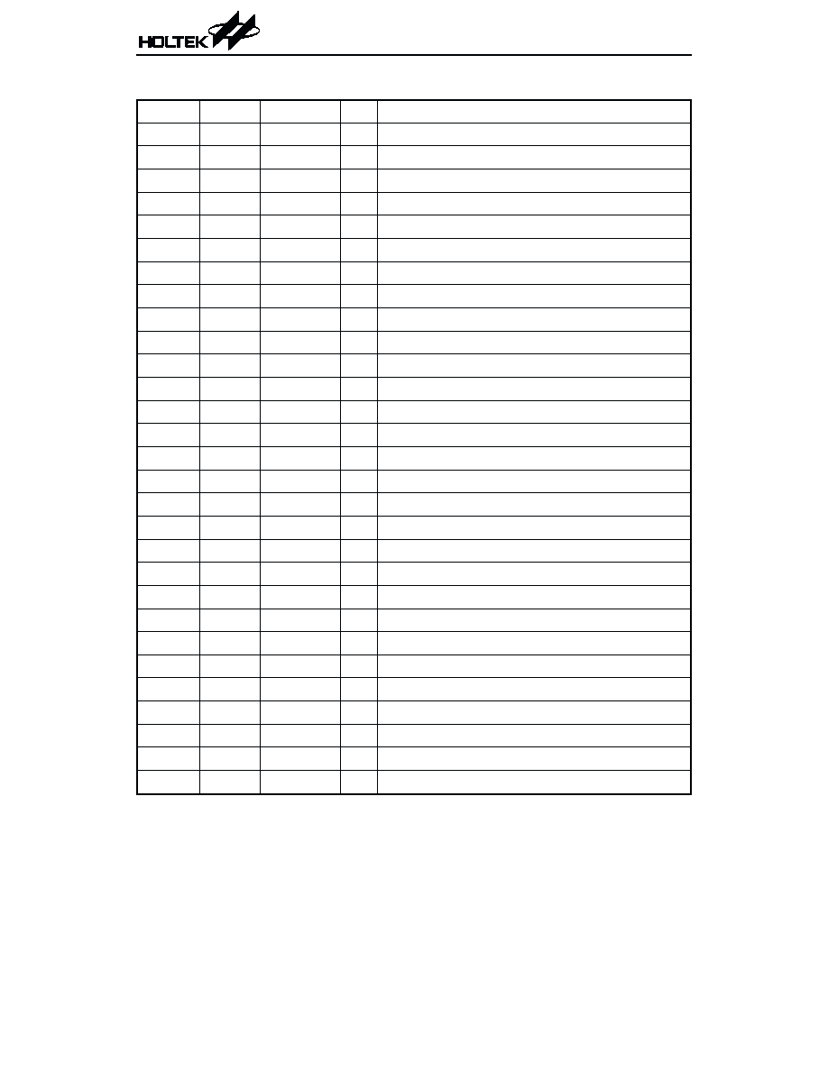
Pad Assignment
Pad Coordinates
Unit: mil
Pad
No.
X
Y
Pad
No.
X
Y
1
-62.7 58.7
16
27.3 -58.7
2
-62.7 48.7
17
37.3 -58.7
3
-62.7 30.1
18
47.3 -58.7
4
-62.7 17.2
19
58.3 -58.7
5
-62.7 7.3
20
62.7 -38.8
6
-62.7 -18.7
21
62.7 -23.7
7
-62.7 -58.7
22
62.7 48.6
8
-52.7 -58.7
23
62.7 58.7
9
-42.7 -58.7
24
43.8 58.7
10
-32.7 -58.7
25
33.8 58.7
11
-22.7 -58.7
26
5.8
58.7
12
-12.7 -58.7
27
-4.3 58.7
13
-2.7 -58.7
28
-38.6 58.7
14
7.3 -58.7
29
-48.6 58.7
15
17.3 -58.7
Chip size: 119 ¥ 112 (mil)
2
* The IC substrate should be connected to VDD in the PCB layout artwork.
Operational Sequence
Note: S1 for Hour setting
S2 for Minute setting
S3 to Start/Stop the timer
S3>5 seconds into the real time setting mode
S1/S2 to reset the timer to the initial state (0:00)
S1/S2/S3 to return to the real time mode
HT1330
2
August 10, 2000
1
1 6
2
1 7
3
1 8
4
1 9
5
2 0
6
2 1
7
2 2
8
2 3
9
2 4
1 0
2 5
1 1
2 6
1 2
2 7
1 3
2 8
1 4
2 9
1 5
( 0 , 0 )
S 3
S 2
S 1
V E E
C A P 2
C A P 1
C O M 1
CO
M
2
KD
1
FE
1
AG
1
BC
1
CO
D3
FE
2
AD
G
2
BC
2
FE
3
AG
3
BC
3
B U S Y
O S C 2
O S C 1
T2
T1
VS
S
VD
D
OP
BZ
BZ
B
P o w e r o n
R e a l T i m e S e t t i n g
U p / D o w n T i m e r
S 3
S 3 > 5 s e c
S 1 o r S 2
S 3
S 3
S 1 / S 2
S 1 / S 2 / S 3
S 1 / S 2
S 1 / S 2 o r S 1 / S 2 / S 3
S 1 / S 2 o r S 1 / S 2 / S 3
C o u n t - d o w n T i m e r
R e a l T i m e
C o u n t - u p T i m e r
C o u n t - d o w n
T i m e S e t t i n g
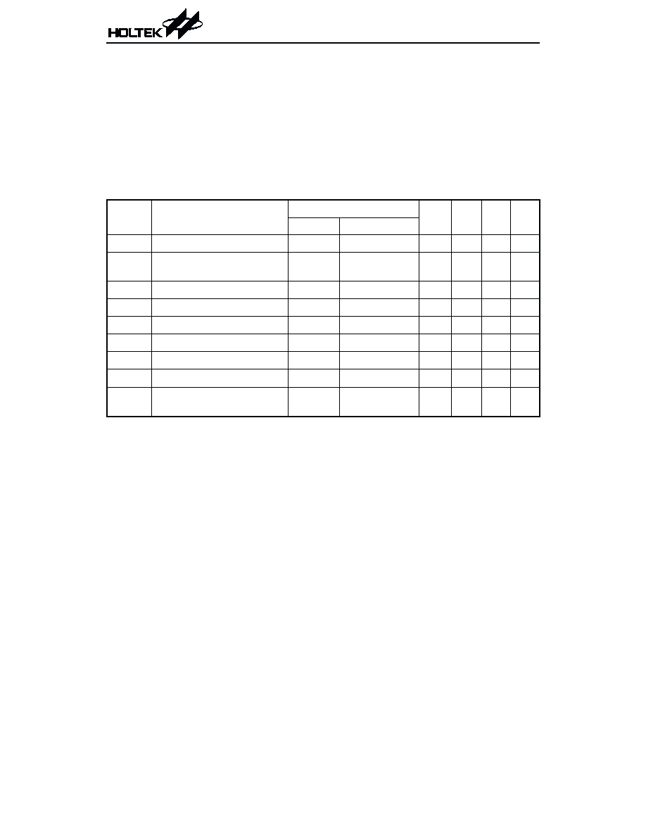
Pin/Pad Description
Pin No. Pad No. Pad Name
I/O
Description
11
1
S3
I
Input to start/stop the timer
14
2
S2
I
Input for minute setting
16
3
S1
I
Input for hour setting
17
4
VEE
æ
Negative voltage supply for LCD display
18
5
CAP2
O
For voltage doubling capacitor
20
6
CAP1
O
For voltage doubling capacitor
24
7
COM1
O
Common 1 drive
25
8
BC3
O
Segment drive
26
9
AG3
O
Segment drive
27
10
FE3
O
Segment drive
28
11
BC2
O
Segment drive
29
12
ADG2
O
Segment drive
30
13
FE2
O
Segment drive
31
14
COD3
O
Segment drive
33
15
BC1
O
Segment drive
34
16
AG1
O
Segment drive
35
17
FE1
O
Segment drive
36
18
KD1
O
Segment drive
37
19
COM2
O
Common 2 drive
38
20
OSC1
I
Oscillator input
39
21
OSC2
O
Oscillator output
46
22
BUSY
O
Timer busy flag, active high
47
23
T2
I/O Chip test pin
4
24
T1
I/O Fast-test control pin
5
25
VSS
æ
Negative power supply
6
26
VDD
æ
Positive power supply
8
27
OP
I
Option pin for countdown recycle
9
28
BZ
O
Piezo drive
10
29
BZB
O
Piezo drive
HT1330
3
August 10, 2000
Absolute Maximum Rating
Supply Voltage.................................-0.3V to 5V
Storage Temperature.................-50∞C to 125∞C
Input Voltage.................V
SS
-0.3V to V
DD
+0.3V
Operating Temperature ................-0∞C to 70∞C
Note: These are stress ratings only. Stresses exceeding the range specified under ≤Absolute Maxi-
mum Ratings≤ may cause substantial damage to the device. Functional operation of this de-
vice at other conditions beyond those listed in the specification is not implied and prolonged
exposure to extreme conditions may affect device reliability.
Electric Characteristics
Ta=25∞C
Symbol
Parameter
Test Conditions
Min. Typ. Max. Unit
V
DD
Conditions
V
DD
Supply Voltage
1.5V
æ
1.25
1.50 1.70
V
I
DD
Operating Current
1.5V
fosc=32768Hz
No load
æ
æ
2
mA
V
EE
Display Voltage
1.25~1.7V
æ
-1.2
-1.5 -1.7
V
I
IN
Switch Input Current
1.5V
V
IN
=VDD
5
æ
65
mA
V
STR
Osc Starting Voltage
æ
Within 3 secs
1.35
æ
æ
V
Df/f
Frequency Stability
1.25~1.7V
æ
æ
æ
10
PPM
I
OHA
Alarm Output Drive Current
1.5V
V
OH
=1.35V
-480
æ
æ
mA
f
OUT
Alarm Output Frequency
1.5V
æ
æ
4096
æ
Hz
I
OHF
Busy Flag Output Drive
Current
1.5V
V
OH
=1.35V
-480
æ
æ
mA
HT1330
4
August 10, 2000
Functional Description
When power is turned on, all the LCD segments
are illuminated to display ≤18:88≤ and the
alarm sounds 2 seconds.
For fast-test, hold the ≤TP1≤ pin high and the
minute digit will be increased every second.
In the count-down mode, when the time has gone
past the set time and the alarm is stopped, the set
time will remain at its current state or be reset to
0:00 depending on the bonding of the ≤OPT≤ pin
to VDD.
In the timer mode, while the timer is counting,
the actual time can be displayed by pressing ≤S1≤.
Once ≤S1≤ is released, the count-down time will
be shown instead.
In the count-up mode, the LCD display is nor-
mally in minutes and seconds where the maxi-
mum count-up period is 20 minutes. If ≤S2≤ is
pressed, the LCD display will revert to hours
and minutes and the maximum count-up time
will turn out to be 20 hours.
The timer alarm will sound during the
count-down process as listed below:
4 sounds are generated at 10 minutes before
the set time is up.
8 sounds are generated at 5 minutes before the
set time is up.

Output Waveform
HT1330
5
August 10, 2000
1 0 m i n u t e s b e f o r e s e t t i m e i s u p
2 s e c
1 s e c
0 s e c
5 m i n u t e s b e f o r e s e t t i m e i s u p
0 s e c
1 s e c
2 s e c
T i m e i s u p
0 s e c
1 s e c
6 0 s e c
T i m e r b u s y f l a g o u t p u t
V D D
V S S
T i m e r i s c o u n t i n g u p o r d o w n
6 2 . 5 m s
6 2 . 5 m s
6 2 . 5 m s
6 2 . 5 m s
6 2 . 5 m s
Once the set time is reached, the alarm will
sound 60 seconds unless it is stopped by users
(by pressing S3), in which case the preset time
of the timer will remain unchanged or at 0:00
depending on the status of the option pin.
Pressing any one of the inputs (S1 or S2 or S3)
will stop the alarm during the period for which
the alarm is sounding.
At 0:00 in the timer mode, the alarm will sound
when S1 and S2 are simultaneously depressed.
This is for the alarm test only.
After the device is powered on, the alarm will
sound two seconds and all segments on the LCD
display panel be illuminated.