 | –≠–ª–µ–∫—Ç—Ä–æ–Ω–Ω—ã–π –∫–æ–º–ø–æ–Ω–µ–Ω—Ç: HT1616C | –°–∫–∞—á–∞—Ç—å:  PDF PDF  ZIP ZIP |
Document Outline
- ˛ˇ
- ˛ˇ
- ˛ˇ
- ˛ˇ
- ˛ˇ
- ˛ˇ
- ˛ˇ
- ˛ˇ
- ˛ˇ
- ˛ˇ
- ˛ˇ
- ˛ˇ

HT1616C
Timer with Dialer Interface
Block Diagram
Rev. 1.10
1
September 13, 2001
Features
∑
Operating voltage: 1.2V~1.7V
∑
Low operating current: 4mA typ.
∑
Dialing number and conversation time display
∑
Conversation timer (59 mins and 59 secs max.)
∑
12 or 16 digits LCD display driver; 3V, 1/2 bias, 1/3
duty
∑
Real time clock
∑
Stop watch
∑
Built-in dialer interface
∑
12-hour or 24-hour format
∑
Two-button sequential operation for real
time clock setting
∑
Uses 32768Hz crystal
Applications
∑
Timers, clocks and watches
∑
LCD display drivers
∑
Telephone display interface
∑
Instrument display
General Description
The HT1616C is a CMOS chip designed for dialer inter-
faces driving 12 or 16-digit LCDs. Various functions,
such as real time clock, dialing number and conversa-
tion time display are provided.
For HT1616C the real time is displayed by default.
When answering a telephone call, the timer is activated
to tell users how long the conversation has taken. After
the telephone is hung up, the total conversation time is
shown for about 5 seconds and the real time is dis-
played again. When making a phone call, the HT1616C
receives dialing data from the dialer and displays the
phone number from left to right on the LCD. However, if
there is no dialing action within 10 seconds, it restarts
the timer again. By adding a TIMER key, the IC can pro-
vide stopwatch and timer reset/hold functions. Refer to
the functional description for details.
Patent Number: 84545 (R.O.C.)
Patent Pending: 08/214, 079 (U.S.A.)
I N T
R E S
D I
S K
H K
S 2
X 1
X 2
T 2
S E G 1
S E G 4 8
C O M 1
C O M 2
C O M 3
V A
V B
V C
T I M E R
S 1
1 2 / 2 4
T i m e
B a s e
T i m e r
S h i f t
R e g i s t e r
S t a t e
C o n t r o l
C o n t r o l
C i r c u i t
C o m m o n
C i r c u i t
D e c o d e r
&
M U X
V o l t a g e
D o u b l e r
S e g m e n t
L a t c h
&
S e l e c t
S c a n
C K T
T 1

Pad Assignment
Chip size: 140.1 ¥ 137.2 (mil)
2
* The IC substrate should be connected to VDD in the PCB layout artwork.
Pad Coordinates
Unit: mil
Pad No.
X
Y
Pad No.
X
Y
Pad No.
X
Y
1
-64.47
61.01
25
-4.11
-61.01
49
64.47
35.53
2
-64.47
50.26
26
4.03
-61.01
50
64.47
41.65
3
-64.47
44.29
27
10.00
-61.01
51
61.60
61.01
4
-64.47
38.33
28
16.01
-61.01
52
55.48
61.01
5
-64.47
32.36
29
22.59
-61.01
53
48.98
61.01
6
-64.47
26.01
30
28.63
-61.01
54
42.86
61.01
7
-64.47
19.55
31
34.63
-61.01
55
36.36
61.01
8
-64.47
13.50
32
40.60
-61.01
56
30.25
61.01
9
-64.47
-2.03
33
46.57
-61.01
57
23.73
61.01
10
-64.47
-8.72
34
52.54
-61.01
58
17.61
61.01
11
-64.47
-15.99
35
58.50
-61.01
59
11.11
61.01
12
-64.47
-22.68
36
64.47
-61.01
60
4.99
61.01
13
-64.47
-29.99
37
64.47
-40.20
61
-1.51
61.01
14
-64.47
-37.67
38
64.47
-34.08
62
-7.63
61.01
15
-64.47
-43.99
39
64.47
-27.58
63
-14.13
61.01
16
-64.47
-50.37
40
64.47
-21.46
64
-20.25
61.01
17
-58.69
-61.01
41
64.47
-14.95
65
-26.75
61.01
18
-52.65
-61.01
42
64.47
-8.84
66
-32.88
61.01
19
-46.53
-61.01
43
64.47
-2.33
67
-39.38
61.01
20
-40.41
-61.01
44
64.47
3.79
68
-45.50
61.01
21
-33.79
-61.01
45
64.47
10.29
69
-52.00
61.01
22
-27.41
-61.01
46
64.47
16.41
70
-58.12
61.01
23
-18.80
-61.01
47
64.47
22.91
24
-12.60
-61.01
48
64.47
29.03
HT1616C
Rev. 1.10
2
September 13, 2001
1
3 6
2
3 7
3
3 8
4
3 9
5
4 0
6
4 1
7
4 2
8
4 3
9
4 4
1 0
4 5
1 1
4 6
1 2
4 7
1 3
4 8
1 4
4 9
1 5
5 0
1 6
5 1
1 7
5 2
1 8
5 3
1 9
5 4
2 0
5 5
2 1
5 6
2 2
5 7
2 3
5 8
2 4
5 9
2 5
6 0
2 6
6 1
2 7
6 2
2 8
6 3
2 9
6 4
3 0
6 5
3 1
6 6
3 2
6 7
3 3
6 8
3 4
6 9
3 5
7 0
( 0 , 0 )
S E G 6
S E G 5
S E G 4
S E G 3
S E G 2
S E G 1
C O M 3
C O M 1
H K
S 1
C L R
M O D E
1 2 / 2 4
S 2
D I
C L K
S E G 3 2
S E G 3 1
S E G 3 0
S E G 2 9
S E G 2 8
S E G 2 7
S E G 3 3
S E G 3 4
S E G 3 5
S E G 3 6
S E G 3 7
S E G 3 8
S E G 3 9
S E G 4 0
SEG
2
6
SEG
2
5
SEG
2
4
SEG
2
3
SEG
2
2
SEG
2
1
SEG
2
0
SEG
1
9
SEG
1
8
SEG
1
7
SEG
1
6
SEG
1
5
SEG
1
4
SEG
1
3
SEG
1
2
SEG
1
1
SEG
1
0
SE
G
9
SE
G
8
SE
G
7
SE
G
4
1
SE
G
4
2
SE
G
4
3
SE
G
4
4
SE
G
4
5
SE
G
4
6
SE
G
4
7
SE
G
4
8
CO
M
2
VD
D
VC
VB
VA
VS
S
IN
T
RE
S
E
T
X2
X1
T2
T1

Pad Description
Pad Name
I/O
Internal
Connection
Description
SEG1~SEG48
O
CMOS OUT
LCD segment signal output pads
COM1~COM3
O
CMOS OUT
LCD common signal output pads
HK
I
CMOS IN
Pull-high
Hook switch detector input
S1
I
CMOS IN
Pull-low
Clock setting switch
Hour or minute can be selected for S2 adjustment
RES
I
CMOS IN
Pull-high
System initialization pin, active low
The pull-high resistance is 200kW typ.
MODE
I
CMOS IN
Pull-low
4 or 5 bits pattern selection pad
VDD: 5 bits pattern
Floating: 4 bits pattern
12/24
I
CMOS IN
Pull-low
12-hour or 24-hour format option pad
VDD: 12-hour format
Floating: 24-hour format
S2
I
CMOS IN
Pull-low
Clock adjusting switch
Hour or minute digits can be adjusted depending upon the S1 selection
DI
I
CMOS IN
Pull-high
Serial data input pad
Data should be valid at the falling edge of SK (connected to the dialer)
SK
I
CMOS IN
Pull-high
Clock input pad (connected to the dialer), active low
Input data is latched at the falling edge of SK
T1
I
CMOS IN
Pull-high
Test pad (connected to VSS for production test)
T2
I
CMOS IN
Pull-high
Test pad (connected to VSS for production test)
X1
I
OSCILLATOR
32768Hz crystal oscillator input
X2
O
32768Hz crystal oscillator output
TIMER
I
CMOS IN
Pull-low
Timer reset-and-start/hold toggle control input pad
INT
O
NMOS OUT
Interrupt output, 16Hz (default) or 2Hz (by mask option)
VA
O
CMOS OUT
Voltage doubler, connected to the external capacitor
VB
O
CMOS OUT
Voltage doubler, connected to the external capacitor
VC
O
CMOS OUT
Voltage doubler, connected to the external capacitor
VDD
æ
æ
Positive power supply
VSS
æ
æ
Negative power supply, ground
Approximate internal connection circuits
HT1616C
Rev. 1.10
3
September 13, 2001
1 2 p F
N M O S O U T
C M O S I N
P u l l - l o w
C M O S I N
P u l l - h i g h
O S C I L L A T O R
C M O S O U T
X 1
X 2
1 5 p F
1 0 M W
V
D D
V
D D

Absolute Maximum Ratings
Supply Voltage ...........................................-0.3V to 5V
Storage Temperature ...........................-50∞C to 125∞C
Input Voltage ............................ V
SS
-0.3V to V
DD
+0.3V
Operating Temperature ..........................-20∞C to 75∞C
Note: These are stress ratings only. Stresses exceeding the range specified under ≤Absolute Maximum Ratings≤ may
cause substantial damage to the device. Functional operation of this device at other conditions beyond those
listed in the specification is not implied and prolonged exposure to extreme conditions may affect device reliabil-
ity.
Electrical Characteristics
f
OSC
=32768Hz, Ta=25∞C
Symbol
Parameter
Test Conditions
Min.
Typ.
Max.
Unit
V
DD
Conditions
V
DD
Operating Voltage
æ
æ
1.2
1.5
1.7
V
V
IL
Input Low Voltage
æ
æ
V
SS
æ
0.2V
DD
V
V
IH
Input High Voltage
æ
æ
0.8V
DD
æ
V
DD
I
STB
Standby Current
1.5V V
HK
=Floating (or V
DD)
æ
0.1
1
mA
I
DD
Operating Current
1.5V No load
æ
4
10
mA
I
OL
Output Sink Current of INT
1.5V V
O
=0.3V
500
1000
æ
mA
t
A
Data Setup Time
1.5V
æ
1
æ
æ
ms
t
B
Data Hold On Time
1.5V
æ
2
æ
æ
ms
t
C
Inter Digit Time
1.5V
æ
5
æ
æ
ms
t
DB
Input Debounce Time (S1, S2, TIMER) 1.5V
æ
æ
31.25
æ
ms
R
HI
Pull-high Resistance (HK, DI, SK)
1.5V V
IN
=0V
æ
1
æ
MW
R
LO
Pull-low Resistance (TIMER)
1.5V V
TIMER
=1.5V
æ
5
æ
MW
f
OSC
System Frequency
1.5V Crystal=32768Hz
æ
32768
æ
Hz
HT1616C
Rev. 1.10
4
September 13, 2001

Functional Description
Operational flow chart
HT1616C
Rev. 1.10
5
September 13, 2001
H K = 0 ?
" H K = 1 "
> 5 s e c s ?
H K = " 0 " ?
N
N
N
Y
Y
N
N
Y
Y
N
Y
Y
H T 1 6 1 6 / H T 1 6 1 6 C : D i s p l a y r e a l t i m e ,
H T 1 6 1 7 : B L A N K
T r i g .
T I M E R k e y ?
N
D i s p l a y d i a l i n g n u m b e r
T i m e r s t o p s , d i s p l a y s
t o t a l c o n v e r s a t i o n t i m e
O v e r 5 s e c s ?
N
Y
Y
N
Y
N
Y
Y
R e s e t t o 0 0 0 0
& s t a r t t i m e r
K e e p c o u n t i n g
T i m e r h o l d
> 5 s e c s ?
N
Y
N
P o w e r - o n
T i m e r k e e p s c o u n t i n g ,
d i s p l a y s t i m e r v a l u e
R e s e t t o 0 0 0 0
& s t a r t t i m e r
D i a l i n g d a t a i n p u t ?
T r i g . T I M E R k e y ?
H K = " 0 " ?
H K = " 0 " ?
N
Y
H K = " 0 " ?
N o
d a t a i n > 1 0 s ?
T r i g . T I M E R k e y ?
T r i g . T I M E R k e y ?
T r i g . T I M E R k e y ?
N
N
Y
Y
R e s e t t o 0 0 0 0
& s t a r t t i m e r
K e e p c o u n t i n g
T i m e r h o l d
T r i g . T I M E R k e y ?
T r i g . T I M E R k e y ?
H K = " 0 " ?
N
N
Y
Y
N
Y
N
Y
H K = 1
> 5 s e c
?
R e s e t t o 0 0 0 0

On-hook & Off-hook
Note: Block A shows the switches S1 and S2 that are used for setting and selecting.
Block B illustrates a timer mode when Off-hook; timer resets and starts to count the conversation time.
Block C displays blinking ≤æ≤. After Off-hook, dialing data is received and displayed on the LCD from left to right.
When the entry interval is over 10 seconds, the timer resets and starts to count.
TIMER key function
The TIMER key is used to start/stop the timer (toggle). In real time mode, it can perform a stop- watch function.
In the conversation timer mode, it can reset or hold the timer.
HT1616C
Rev. 1.10
6
September 13, 2001
B l o c k A
B l o c k B
B l o c k C
R e c e i v e D i g i t ( s )
7 8
7
7 8 0
O n - h o o k
R e c e i v e D a t a
N o D a t a
E n t r y > 1 0 s e c s
0 0 0 0
T i m e r M o d e
O n - h o o k
0 0 0 1
0 0 0 2
1 1
2 6
1 0 2 5 3 7
S 2
S 2
S 2
S 1
S 1
H o u r
M i n u t e
R e a l T i m e
D i s p l a y T i m e r
5 - s e c d u r a t i o n
> 5 s e c s
< 5 s e c s a n d
O f f - h o o k
O f f - h o o k
T r i g . T I M E R
( w i t h i n 5 s e c s )
T i m e r r e s e t
a n d c o u n t
0 0 0 0
0 1 2 4
T r i g .
T I M E R
0 1 2 4
T i m e r h o l d
N o a c t i o n f o r
o v e r 5 s e c s
T i m e r r e s e t
a n d c o u n t
0 0 0 0
0 0 1 2
L C D d i s p l a y
r e a l t i m e
1 0 1 1 0 0
0 0 1 2 3 6
R e t u r n t o r e a l
t i m e c l o c k
0 0 1 2
T i m e r h o l d
T r i g . T I M E R
T r i g . T I M E R
D i a l i n g o u t
T i m e r r e s e t
a n d c o u n t
0 0 0 0
0 1 2 4
T r i g .
T I M E R
T i m e r r e s e t
a n d c o u n t
0 0 0 0
0 0 1 2
L C D d i s p l a y
r e a l t i m e
1 0 1 1 0 0
1 2 3 4 5 6 7
D i a l f i n i s h e d
( a f t e r 1 0 s e c s )
0 1 2 4
T i m e r h o l d
0 0 2 4 3 6
H T 1 6 1 6 C
R e t u r n t o r e a l
t i m e c l o c k
O n - h o o k f o r
o v e r 5 s e c s
T r i g . T I M E R
T i m e r r e s e t
a n d c o u n t
0 0 0 0
0 1 2 4
S h o w d i a l i n g
n u m b e r s
( H K = 0 )
O f f - h o o k

HT1616C
Rev. 1.10
7
September 13, 2001
Data & Timing
∑
For telephone application
The HT1616C is designed to display telephone num-
bers derived from the HT93XXX series telephone di-
aler ICs. When the MODE pad is connected to VSS,
the corresponding data is illustrated in the following
table (MODE=0).
∑
For instrument or mc application
The HT1616C is also capable of displaying BCD data
generated from instrument or a mC system. The corre-
sponding data and timing is shown in the Data Latch Tim-
ing diagram. Before the data is transmitted to the
HT1616C, the HK pin should be pulled-low or continu-
ously kept low. The HT1616C is then ready to receive the
data. At the falling edge of the clock the data is shifted in
to the IC. After all the data is sent to the HT1616C, the SK
pin is set low to avoid switching to the timer mode.
When the MODE pad is connected to ≤Low≤, the data
code and display patterns are shown in the following
table:
K e y - I n
D a t a C o d e
D i s p l a y
b 3
b 2
b 1
b 0
B l a n k
1
2
3
4
5
6
7
8
9
0
*
#
F
P
1
0
0
0
0
0
0
0
0
1
1
1
1
1
1
1
1
1
0
1
1
0
0
0
1
1
1
1
0
0
0
0
0
0
0
1
1
1
0
1
0
1
0
1
0
1
0
1
0
1
0
1
1
1
1
0
0
1
0
0
1
1
0
0
B l a n k
D a t a C o d e
D i s p l a y
b 3
b 2
b 1
b 0
1
0
0
0
0
0
0
0
0
1
1
1
1
1
1
1
1
1
0
1
1
0
0
0
1
1
1
1
0
0
0
0
0
0
0
1
1
1
0
1
0
1
0
1
0
1
0
1
0
1
0
1
1
1
1
0
0
1
0
0
1
1
0
0
B l a n k

On the other hand, when MODE pad is connected to ≤High≤ the data code and display patterns are shown in the follow-
ing table:
(MODE=1)
(MODE=1)
∑
Data latch timing for 4-bit pattern (MODE=0)
∑
Data latch timing for 5-bit pattern (MODE=1)
HT1616C
Rev. 1.10
8
September 13, 2001
D a t a C o d e
D i s p l a y
b 3
b 2
b 1
b 0
1
0
0
0
0
0
0
0
0
1
1
1
1
1
1
1
1
1
0
1
1
0
0
0
1
1
1
1
0
0
0
0
0
0
0
1
1
1
0
1
0
1
0
1
0
1
0
1
0
1
0
1
1
1
1
0
0
1
0
0
1
1
0
0
b 4
1
1
1
1
1
1
1
1
1
1
1
1
1
1
1
1
D a t a C o d e
D i s p l a y
b 3
b 2
b 1
b 0
1
0
0
0
0
0
0
0
0
1
1
1
1
1
1
1
1
1
0
1
1
0
0
0
1
1
1
1
0
0
0
0
0
0
0
1
1
1
0
1
0
1
0
1
0
1
0
1
0
1
0
1
1
1
1
0
0
1
0
0
1
1
0
0
B l a n k
b 4
0
0
0
0
0
0
0
0
0
0
0
0
0
0
0
0
C L K
D I
D i g i t 1
D i g i t 2
D i g i t N
b 3
b 0
b 1
b 2
b 3
b 0
b 1
b 2
b 0
b 1
t
B
t
A
t
C
C L K
D I
D i g i t 1
D i g i t 2
D i g i t N
b 4
b 1
b 2
b 4
b 0
b 1
b 0
b 3
b 0
b 3
b 1
b 2
t
B
t
A
t
C

Application Circuits
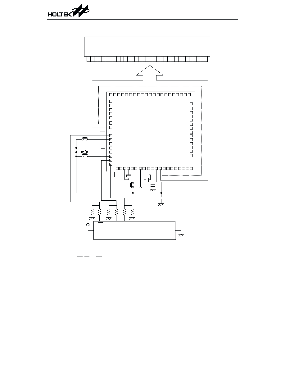
For telephone interfacing (with batteries)
* The IC substrate should be connected to VDD in the PCB layout artwork.
HT1616C
Rev. 1.10
9
September 13, 2001
H D I
SK
H K
1 2 / 2 4
1 2 / 1 6 - D i g i t L C D
C O M S E G
C O M
S E G C O M
3 0
2
1
3
1
S 2
S 1
3 2 7 6 8 H z
1
2
3
4
5
6
7
8
9
1 0
1 1
1 2
1 3
1 4
1 5
1 6 1 7 1 8 1 9 2 0 2 1 2 2 2 3 2 4 2 5 2 6 2 7 2 8 2 9 3 0 3 1 3 2 3 3 3 4 3 5
4 9
4 8
4 7
4 6
4 5
4 4
4 3
4 2
4 1
4 0
3 9
3 8
3 7
3 6
7 0
6 9 6 8 6 7 6 6 6 5 6 4 6 3 6 2 6 1 6 0 5 9 5 8 5 7 5 6 5 5 5 4 5 3 5 2 5 1
5 0
H T 1 6 1 6 C
0 . 1 m F
TI
M
E
R
D I
P O
D O
C L O C K
4 7 k W
H T 9 3 X X X D i a l e r
H F O
8 0 5 0
0 . 0 2 m F
H F I
3 3 0 m F
1 0 V
V S S
1 A b r i d g e
R i n g
T i p
A 9 2
H F I
V D D
8 0 5 0
A 4 2
5 . 1 V
1 0 M W
H K S
1 N 4 1 4 8 ¥ 3
3 3 0 k W
2 7 0 k W
2 2 0 k W
1 0 0 k W
4 7 k W
2 . 7 k W
3 3 k W
4 7 k W
1 0 0 k W
O f f - h o o k
O n - h o o k
H D I
V S S
X 1
X 2
1 . 5 V
3 . 5 8 M H z
0 . 1 m F

For telephone interfacing (without batteries)
* The IC substrate should be connected to VDD in the PCB layout artwork.
HT1616C
Rev. 1.10
10
September 13, 2001
P O
H K
1
2
3
4
5
6
7
8
9
1 0
1 1
1 2
1 3
1 4
1 5
1 6 1 7 1 8 1 9 2 0 2 1 2 2 2 3 2 4 2 5 2 6 2 7 2 8 2 9 3 0 3 1 3 2 3 3 3 4 3 5
4 9
4 8
4 7
4 6
4 5
4 4
4 3
4 2
4 1
4 0
3 9
3 8
3 7
3 6
7 0
6 9 6 8 6 7 6 6 6 5 6 4 6 3 6 2 6 1 6 0 5 9 5 8 5 7 5 6 5 5 5 4 5 3 5 2 5 1
5 0
H T 1 6 1 6 C
H K S
0 . 1 m F
1 2 / 1 6 - D i g i t L C D
C O M S E G
C O M
S E G C O M
3 0
2
1
3
1
TI
M
E
R
3 2 7 6 8 H z
D O
C L O C K
4 7 k W
H T 9 3 X X X D i a l e r
H F O
8 0 5 0
0 . 0 2 m F
H F I
3 3 0 m F
1 0 V
V S S
1 A b r i d g e
R i n g
T i p
A 9 2
H F I
V D D
8 0 5 0
A 4 2
5 . 1 V
1 0 M W
1 m F
1 N 4 1 4 8 ¥ 6
SK
D I
3 3 0 k W
2 7 0 k W
2 2 0 k W
1 0 0 k W
2 0 k W
4 7 k W
4 7 k W
1 0 0 k W
2 . 7 k W
3 3 k W
O f f - h o o k
O n - h o o k
V S S
X 1
X 2
3 . 5 8 M H z
H D I
H D I
0 . 1 m F
For instrument or mC use
* The IC substrate should be connected to VDD in the PCB layout artwork.
Note:
To drive SK, DI and HK , an open drain NMOS output structure is recommended.
To drive SK, DI and HK with a CMOS output structure, a voltage divider is needed (R=4.3kW, R1=10kW).
HT1616C
Rev. 1.10
11
September 13, 2001
TI
M
E
R
H K
1 2 / 2 4
1 2 / 1 6 - D i g i t L C D
C O M S E G
C O M
S E G C O M
3 0
2
1
3
1
S 2
S 1
3 2 7 6 8 H z
1
2
3
4
5
6
7
8
9
1 0
1 1
1 2
1 3
1 4
1 5
1 6 1 7 1 8 1 9 2 0 2 1 2 2 2 3 2 4 2 5 2 6 2 7 2 8 2 9 3 0 3 1 3 2 3 3 3 4 3 5
4 9
4 8
4 7
4 6
4 5
4 4
4 3
4 2
4 1
4 0
3 9
3 8
3 7
3 6
7 0
6 9 6 8 6 7 6 6 6 5 6 4 6 3 6 2 6 1 6 0 5 9 5 8 5 7 5 6 5 5 5 4 5 3 5 2 5 1
5 0
H T 1 6 1 6 C
D O
C L O C K
V D D
1 . 5 V
H K
5 V
V S S
I n s t r u m e n t o r m C S y s t e m
R 1
R
R 1
R
R 1
R
0 . 1 m F
SK
D I
+
0 . 1 m F

LCD Configurations
For 12-digit application
∑
Segment electrode side
LCD driving system 1/2 bias, 1/3 duty, 3V
∑
Common electrode side
∑
LCD connection
For 16-digit application
∑
Segment electrode side
LCD driving system 1/2 bias, 1/3 duty, 3V
∑
Common electrode side
∑
LCD connection
HT1616C
Rev. 1.10
12
September 13, 2001
S E G
1 3
S E G
1 4
S E G
1 5
S E G
1 6
C O M
1
C O M
3
C O M
2
S E G
4 8
S E G
4 7
1 3 1 4 1 5
3 9
4 0 4 1 4 2
3 3
3 4 3 5 3 6
3 7 3 8
2 9 3 0
3 1 3 2
S E G
1 6 1 7 1 8
1 9 2 0 2 1
2 2 2 3 2 4
2 5 2 6 2 7
2 8
4 3 4 4 4 5
4 6 4 7 4 8
C O M 1
C O M 2
C O M 3
C O M 1
C O M 2
C O M 3
7 8 9
2 7 2 8 2 9 3 0
2 1 2 2 2 3 2 4 2 5 2 6
1 5
1 6 1 7 1 8
1 9 2 0
1 0 1 1 1 2 1 3 1 4
S E G
4 5 6
1 2 3
3 1 3 2 3 3 3 4 3 5 3 6
3 7 3 8 3 9 4 0 4 1 4 2 4 3 4 4 4 5 4 6 4 7 4 8
S E G
4 7
S E G
S E G
S E G
S E G
C O M
2
1
1
4
5
6
S E G
S E G
C O M
3
3
S E G
4 5
S E G
4 6
S E G
4 8
C O M
2

HT1616C
Rev. 1.10
13
September 13, 2001
Copyright
” 200
1
by HOLTEK SEMICONDUCTOR INC.
The information appearing in this Data Sheet is believed to be accurate at the time of publication. However, Holtek as-
sumes no responsibility arising from the use of the specifications described. The applications mentioned herein are used
solely for the purpose of illustration and Holtek makes no warranty or representation that such applications will be suitable
without further modification, nor recommends the use of its products for application that may present a risk to human life
due to malfunction or otherwise. Holtek
¢s products are not authorized for use as critical components in life support devices
or systems. Holtek reserves the right to alter its products without prior notification. For the most up-to-date information,
please visit our web site at http://www.holtek.com.tw.
Holtek Semiconductor Inc. (Headquarters)
No.3, Creation Rd. II, Science Park, Hsinchu, Taiwan
Tel: 886-3-563-1999
Fax: 886-3-563-1189
http://www.holtek.com.tw
Holtek Semiconductor Inc. (Taipei Sales Office)
4F-2, No. 3-2, YuanQu St., Nankang Software Park, Taipei 115, Taiwan
Tel: 886-2-2655-7070
Fax: 886-2-2655-7373
Fax: 886-2-2655-7383 (International sales hotline)
Holtek Semiconductor Inc. (Shanghai Sales Office)
7th Floor, Building 2, No.889, Yi Shan Rd., Shanghai, China 200233
Tel: 021-6485-5560
Fax: 021-6485-0313
http://www.holtek.com.cn
Holtek Semiconductor Inc. (Shenzhen Sales Office)
43F, SEG Plaza, Shen Nan Zhong Road, Shenzhen, China 518031
Tel: 0755-8346
-
5589
Fax: 0755-8346
-
5590
ISDN: 0755-8346
-
5591
Holtek Semiconductor Inc. (Beijing Sales Office)
Suite 1721, Jinyu Tower, A129 West Xuan Wu Men Street, Xicheng District, Beijing, China 100031
Tel: 010-6641
-
0030, 6641
-
7751, 6641
-
7752
Fax: 010-6641
-
0125
Holmate Semiconductor, Inc. (North America Sales Office)
46712 Fremont Blvd., Fremont, CA 94538
Tel: 510-252-9880
Fax: 510-252-9885
http://www.holmate.com