 | –≠–ª–µ–∫—Ç—Ä–æ–Ω–Ω—ã–π –∫–æ–º–ø–æ–Ω–µ–Ω—Ç: HT16515 | –°–∫–∞—á–∞—Ç—å:  PDF PDF  ZIP ZIP |
Document Outline
- ˛ˇ
- ˛ˇ
- ˛ˇ
- ˛ˇ
- ˛ˇ
- ˛ˇ
- ˛ˇ
- ˛ˇ
- ˛ˇ
- ˛ˇ
- ˛ˇ
- ˛ˇ
- ˛ˇ
- ˛ˇ
- ˛ˇ

HT16515
1/4 to 1/12 Duty VFD Controller
Block Diagram
Rev. 1.00
1
December 19, 2003
Features
∑
Logic voltage: 5V
∑
High-voltage output: V
DD
-35V max.
∑
Multiple display
(16-segment & 12-digit to 24-segment & 4-digit)
∑
16
¥2 matrix key scanning
∑
8 steps dimmer circuit
∑
4 LED output ports (20mA max.)
∑
No external resistors necessary for driver output
(provides PMOS open-drain and pull-low resistor
output)
∑
Serial interface with MCU (CLK, CS, DI, DO)
∑
44-pin QFP package
Applications
∑
Consumer products panel function control
∑
Industrial measuring instrument panel function control
∑
Other similar applications for panel function control
General Description
HT16515 is a VFD (Vacuum Fluorescent Display) con-
troller/driver that is driven on a 1/4 to 1/12 duty factor. It
consists of 16 segment output lines, 4 grid output lines,
8 segment/grid output drive lines, 4 LED output ports, a
control circuit, a display memory, and a key scan circuit.
Serial data inputs to the HT16515 through a three-line
serial interface. This VFD controller/driver is an ideal
MCU peripheral device.
D I
S e r i a l I / F
D i s p l a y R A M
2 4 - B i t ¥ 1 2 W o r d s
T i m i n g G e n e r a t o r
K e y S c a n
K e y D a t a M e m o r y
( 2 ¥ 1 6 )
O S C
4 - B i t L a t c h
S e g 1 / K S 1
L E D 0 ~ L E D 3
C S
C L K
D O
O S C
2 4 - B i t
O u t p u t L a t c h
S e g m e n t
D r i v e r
2 4
1 6
K e y 0 ~ K e y 1
1 2 - B i t
S h i f t R e g i s t e r
M u l t i p l e x e d
D r i v e r
G r i d
D r i v e r
1 2
4
8
8
D i m m i n g C i r c u i t
D a t a
S e l e c t o r
8
V D D
V S S
V E E
C o m m a n d D e c o d e r
S e g 1 6 / K S 1 6
S e g 1 7 / G r i d 1 2
S e g 2 4 / G r i d 5
G r i d 1
G r i d 4
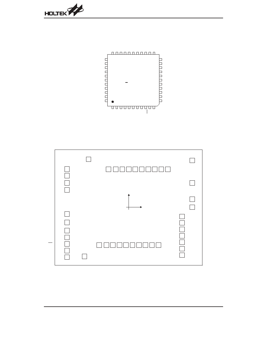
Pin Assignment
Pad Assignment
Chip Size:
* The IC substrate should be connected to VSS in the PCB layout artwork.
HT16515
Rev. 1.00
2
December 19, 2003
1
2
3
4
5
6
7
8
9 1 0 1 1
1 2
1 3
1 4
1 5
1 6
1 7
1 8
1 9
2 0
2 1
2 2
2 3
2 4
2 5
2 6
2 7
2 8
2 9
3 0
3 1
3 2
3 3
3 4
3 5
3 6
3 7
3 8
3 9
4 0
4 1
4 2
4 3
4 4
0 6 $ # #
" " 3 . 2
L
E
D
0
L
E
D
1
L
E
D
2
L
E
D
3
O
S
C
D
O
D
I
C
L
K
C
S
K
E
Y
0
K
E
Y
1
V S S
S e g 1 / K S 1
S e g 2 / K S 2
S e g 3 / K S 3
S e g 4 / K S 4
S e g 5 / K S 5
S e g 6 / K S 6
S e g 7 / K S 7
S e g 8 / K S 8
S e g 9 / K S 9
V D D
S
e
g
1
0
/
K
S
1
0
S
e
g
1
1
/
K
S
1
1
S
e
g
1
2
/
K
S
1
2
S
e
g
1
3
/
K
S
1
3
S
e
g
1
4
/
K
S
1
4
S
e
g
1
5
/
K
S
1
5
S
e
g
1
6
/
K
S
1
6
V
E
E
S
e
g
1
7
/
G
r
i
d
1
2
S
e
g
1
8
/
G
r
i
d
1
1
S
e
g
1
9
/
G
r
i
d
1
0
S e g 2 0 / G r i d 9
S e g 2 1 / G r i d 8
S e g 2 2 / G r i d 7
S e g 2 3 / G r i d 6
S e g 2 4 / G r i d 5
G r i d 4
G r i d 3
G r i d 2
G r i d 1
V D D
V S S
( 0 , 0 )
1
2
3
4
5
6
7
8
9
1 0
1 1
1 2
1 3
1 4
1 5
1 6
1 7
1 8
1 9
2 0
2 1
2 2
2 9
2 8
2 7
2 6
2 5
2 4
2 3
3 3
3 2
3 1
3 0
3 4
3 5
3 6
3 7
3 8
3 9
4 0
4 1
4 2
4 3
4 4
L E D 0
L E D 1
L E D 2
L E D 3
O S C
D O
D I
C L K
C S
K E Y 0
K E Y 1
V
S
S
S
e
g
1
/
K
S
1
S
e
g
2
/
K
S
2
S
e
g
3
/
K
S
3
S
e
g
4
/
K
S
4
S
e
g
5
/
K
S
5
S
e
g
6
/
K
S
6
S
e
g
7
/
K
S
7
S
e
g
8
/
K
S
8
S
e
g
9
/
K
S
9
S e g 1 0 / K S 1 0
S e g 1 1 / K S 1 1
S e g 1 2 / K S 1 2
S e g 1 3 / K S 1 3
S e g 1 4 / K S 1 4
S e g 1 5 / K S 1 5
S e g 1 6 / K S 1 6
V
D
D
V E E
S e g 1 7 / G r i d 1 2
S e g 1 8 / G r i d 1 1
S e g 1 9 / G r i d 1 0
S
e
g
2
0
/
G
r
i
d
9
S
e
g
2
1
/
G
r
i
d
8
S
e
g
2
2
/
G
r
i
d
7
S
e
g
2
3
/
G
r
i
d
6
S
e
g
2
4
/
G
r
i
d
5
G
r
i
d
4
G
r
i
d
3
G
r
i
d
2
G
r
i
d
1
V
D
D
V
S
S
Pad Coordinates
Unit:
mm
Pad No.
X
Y
Pad No.
X
Y
1
-962.50
600.00
23
834.10
-754.00
2
-962.50
495.00
24
834.10
-652.60
3
-962.50
380.20
25
834.10
-551.20
4
-962.50
275.20
26
834.10
-449.80
5
-962.50
-107.20
27
834.10
-348.40
6
-962.50
-235.60
28
834.10
-247.00
7
-962.50
-366.00
29
834.10
-145.60
8
-962.50
-471.00
30
987.30
0.50
9
-962.50
-576.00
31
987.30
130.50
10
-962.50
-681.00
32
987.30
382.05
11
-962.50
-786.00
33
987.30
734.05
12
-689.60
-772.45
34
610.30
594.40
13
-460.45
-595.30
35
508.90
594.40
14
-344.25
-595.30
36
407.50
594.40
15
-242.85
-595.30
37
306.10
594.40
16
-141.45
-595.30
38
204.70
594.40
17
-40.05
-595.30
39
103.30
594.40
18
61.35
-595.30
40
1.90
594.40
19
162.75
-595.30
41
-99.50
594.40
20
264.15
-595.30
42
-200.90
594.40
21
365.55
-595.30
43
-317.10
594.40
22
466.95
-595.30
44
-624.50
756.80
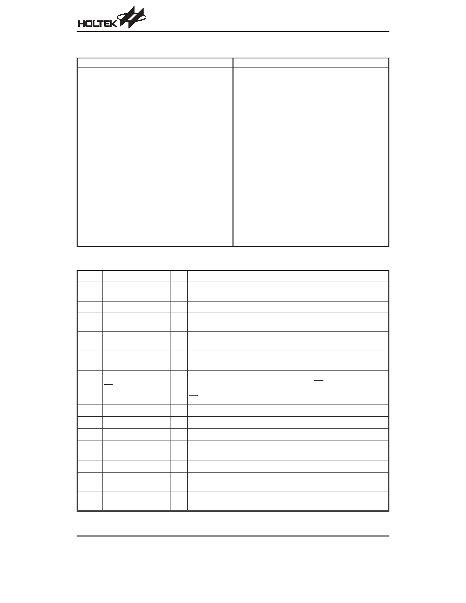
Pin Description
Pin No.
Pin Name
I/O
Description
1~4
LED3~LED0
O
LED driver output ports. This is a CMOS output pin and maximum driving
current up to +20mA.
5
OSC
I
Connected to an external resistor or an RC oscillator circuit.
6
DO
O
Data output pin, output serial data at falling edge of shift clock, starting from
the lower bit. This is N-ch open-drain output pin.
7
DI
I
Data input pin, input serial data at rising edge of shift clock, starting from the
lower bit.
8
CLK
I
Clock input pin. Reads serial data at the rising edge, and outputs data at the
falling edge.
9
CS
I
Initializes serial interface at the rising or falling edge of the HT16515. Then
it waits to receive a command. Data input after CS has fallen is processed,
current processing is stopped, and the serial interface is initialized. While
CS is high, CLK is ignored.
10, 11
Key0, Key1
I
Key-in data input to these pins are latched at the end of the display cycle.
12, 44
VSS
æ Negative power supply, ground
13, 43
VDD
æ Positive power supply
14~29
Seg1/KS1~Seg16/KS16
O
High voltage output, segment output pins, dual function as key source. This
is PMOS open-drain and pull-low resistor output.
30
VEE
æ VFD power supply
31~38
Seg17/Grid12~
Seg24/Grid5
O
High voltage output, these pins are selectable for segment or grid output.
This is PMOS open-drain and pull-low resistor output.
39~42
Grid4~Grid1
O
High voltage output, grids output pin. This is PMOS open-drain and pull-low
resistor output.
HT16515
Rev. 1.00
3
December 19, 2003

Approximate Internal Connections
Absolute Maximum Ratings
Supply Voltage ...........................V
SS
-0.3V to V
SS
+6.0V
Operating Temperature...........................
-25∞C to 75∞C
Input Voltage..............................V
SS
-0.3V to V
DD
+0.3V
Storage Temperature ............................
-50∞C to 125∞C
Note: These are stress ratings only. Stresses exceeding the range specified under
≤Absolute Maximum Ratings≤ may
cause substantial damage to the device. Functional operation of this device at other conditions beyond those
listed in the specification is not implied and prolonged exposure to extreme conditions may affect device reliabil-
ity.
D.C. Characteristics
Ta=25
∞C
Symbol
Parameter
Test Conditions
Min.
Typ.
Max.
Unit
V
DD
Conditions
V
DD
Logic Supply Voltage
æ
æ
4.5
5
5.5
V
V
EE
VFD Supply Voltage
æ
æ
0
æ
V
DD
-35
V
f
OSC
Oscillation Frequency
5V
R
OSC
=82k
W
350
500
650
kHz
R
PL
Output Pull-low Resistor
5V
Driver output
40
65
120
k
W
I
DD
Operating Current
5V
No load, VFD display off
æ
æ
5
mA
I
OL
Driver Leakage Current
5V
V
O
=V
DD
-30V, VFD driver off
æ
æ
-10
mA
I
OL1
LED Sink Current
5V
V
OL
=1V, LED0~LED3
20
æ
æ
mA
I
OH1
LED Source Current
5V
V
OH
=0.9V
DD
, LED0~LED3
-3
æ
æ
mA
I
OH21
Segment 1~16 Source Current 5V
V
OH
=V
DD
-2V
-3
æ
æ
mA
I
OH22
Segment 17~24, Grid 1~4
Source Current
5V
V
OH
=V
DD
-2V
-15
æ
æ
mA
I
OL3
DO Sink Current
5V
V
OL
=0.4V
4
æ
æ
mA
V
IH
≤H≤ Input Voltage
æ
æ
0.7V
DD
æ
V
DD
V
V
IL
≤L≤ Input Voltage
æ
æ
0
æ
0.3V
DD
V
V
H
Hysteresis Voltage
æ CLK, D
IN
, CS
æ
0.35
æ
V
V
OH1
High-level Output Voltage
5V
LED0~LED3, I
OH1
=
-3mA
0.9V
DD
æ
V
DD
V
V
OL1
Low-level Output Voltage
5V
LED0~LED3, I
OL1
=20mA
0
æ
1
V
V
OL2
Low-level Output Voltage
5V
DO, I
OL2
=4mA
0
æ
0.4
V
HT16515
Rev. 1.00
4
December 19, 2003
N M O S O U T
V
D D
P M O S O U T
C M O S O U T
V
D D
V
E E

A.C. Characteristics
Ta=25
∞C
Symbol
Parameter
Test Conditions
Min.
Typ.
Max.
Unit
V
DD
Conditions
t
PHL
Logic Supply Voltage
5V
CLK
ÆDO
C
L
=15pF, R
L
=10k
W
æ
æ
300
ns
t
PLH
5V
æ
æ
300
ns
t
r1
Rise Time
5V
C
L
=300pF, S1~S16
æ
æ
2
ms
t
r2
5V
C
L
=300pF, G1~G4
S17/G12~S24/G5
æ
æ
0.5
ms
t
f
Fall Time
5V
C
L
=300pF, Sn, Gn
æ
æ
120
ms
t
max
Maximum Clock Frequency
5V
Duty=50%
1
æ
æ
MHz
C
i
Input Capacitance
5V
æ
æ
æ
15
pF
t
CW
Clock Pulse Width
5V
æ
400
æ
æ
ns
t
SW
Strobe Pulse Width
5V
æ
1
æ
æ
us
t
SU
Data Setup Time
5V
æ
100
æ
æ
ns
t
h
Data Hold Time
5V
æ
100
æ
æ
ns
t
CS
Clock-Strobe Time
5V
CLK rising edge to CS rising edge
1
æ
æ
ms
t
W
Wait Time
5V
CLK rising edge to CLK falling edge
1
æ
æ
ms
HT16515
Rev. 1.00
5
December 19, 2003
Functional Description
Display RAM and Display Mode
The static display RAM stores the data transmitted from
an external device to the HT16515 through a serial inter-
face. The contents of the RAM are directly mapped to
the contents of the VFD driver. Data in the RAM can be
accessed through the data setting, address setting and
display control commands. It is assigned as addresses
in 8-bit unit as follows:
Dimming Control
HT16515 provides an 8-step dimmer function on display
by controlling the 3-bit binary command code. The full
pulse width of grid signal is divided into 16 uniform sec-
tions by PWM (pulse width modulation) technology.
The 16 uniform sections available form an 8-step dim-
mer via 3-bit binary code. The 8-step dimmer includes
1/16, 2/16, 4/16, 10/16, 11/16, 12/16, 13/16 and 14/16.
The 1/16 pulse width indicates minimum lightness. The
14/16 pulse width represents maximum lightness (Refer
to the display control command).
Key Matrix and Key-Input Data Storage RAM
The key matrix scans the series key states at each level
of the key strobe signal (Seg1/K1~Seg16/K16) output of
the HT16515. The key strobe signal outputs are
time-multiplexed signals from Seg1/K1~Seg16/K16.
The states of inputs K0 and K1 are sampled by strobe
signal Seg1/K1~Seg16/K16 and latched into the regis-
ter.
0 1 H
U
0 4 H
U
0 7 H
U
0 A H
U
0 D H
U
1 0 H
U
1 3 H
U
1 6 H
U
1 9 H
U
1 C H
U
1 F H
U
2 2 H
U
0 0 H
L
0 3 H
L
0 6 H
L
0 9 H
L
0 C H
L
0 F H
L
1 2 H
L
1 5 H
L
1 8 H
L
1 B H
L
1 E H
L
2 1 H
L
0 0 H
U
0 3 H
U
0 6 H
U
0 9 H
U
0 C H
U
0 F H
U
1 2 H
U
1 5 H
U
1 8 H
U
1 B H
U
1 E H
U
2 1 H
U
S E G 1
S E G 4
S E G 8
S E G 1 2
S E G 1 6
S E G 2 0
0 1 H
L
0 4 H
L
0 7 H
L
0 A H
L
0 D H
L
1 0 H
L
1 3 H
L
1 6 H
L
1 9 H
L
1 C H
L
1 F H
L
2 2 H
L
0 2 H
L
0 5 H
L
0 8 H
L
0 B H
L
0 E H
L
1 1 H
L
1 4 H
L
1 7 H
L
1 A H
L
1 D H
L
2 0 H
L
2 3 H
L
D I G 1
D I G 2
D I G 3
D I G 4
D I G 5
D I G 6
D I G 7
D I G 8
D I G 9
D I G 1 0
D I G 1 1
D I G 1 2
X X H
L
X X H
U
b 0
b 3 b 4
b 7
L o w e r
4 b i t s
H i g h e r
4 b i t s
0 2 H
U
0 5 H
U
0 8 H
U
0 B H
U
0 E H
U
1 1 H
U
1 4 H
U
1 7 H
U
1 A H
U
1 D H
U
2 0 H
U
2 3 H
U
S E G 2 4