 | ÐлекÑÑоннÑй компоненÑ: HT1660 | СкаÑаÑÑ:  PDF PDF  ZIP ZIP |
Äîêóìåíòàöèÿ è îïèñàíèÿ www.docs.chipfind.ru
HT1660
96´32 LCD Controller for I/O MCU
Rev. 1.00
1
September 16, 2003
Features
·
Operating voltage: 2.7V~5.2V
·
Built-in 32kHz RC oscillator
·
External 32.768kHz crystal oscillator or 32kHz fre-
quency source input
·
Standby current: <1
mA at 3V, <2mA at 5V
·
Internal resistor type: 1/6 bias or 1/5 bias, 1/32 duty,
or 1/16 duty
·
Three selectable LCD frame frequencies: 64Hz,
89Hz or 170Hz
·
Max. 96
´32 patterns, 96 segments and 32 commons
·
112 segments and 16 commons selectable by com-
mand method
·
Built-in bit-map display RAM: 3072 bits (=96
´32 bits)
·
Built-in internal resistor type bias generator
·
Six-wire interface (four data wires)
·
Eight kinds of time base/WDT selection
·
Time base or WDT overflow output
·
R/W address auto increment
·
Built-in buzzer driver (2kHz/4kHz)
·
Power down command reduces power consumption
·
Software configuration feature
·
Data mode and Command mode instructions
·
Three data accessing modes
·
Provides VLCD pin to adjust LCD operating voltage
and max. VLCD voltage up to 7V
·
Provides three kinds of bias current programming
·
Control of TN-type and STN-type LCDs
·
160-pin QFP package
General Description
HT1660 is a peripheral device specially designed for I/O
type MCU used to expand the display capability. The
max. display segment of the device are 3072 patterns
(96 segments and 32 commons). It also supports four
data bits interface, buzzer sound, Watchdog Timer or
time base timer functions. The HT1660 is a memory
mapping and multi-function LCD controller. Since the
HT1660 can control TN-type (Twisted Nematic) or
STN-type (Super Twisted Nematic) LCDs. The software
configuration feature of the HT1660 make it suitable for
multiple LCD applications including LCD modules and
display subsystems. Only six lines (CS, WR, DB0~DB3)
are required for the interface between the host controller
and the HT1660.
Applications
·
Leisure products
·
Games
·
Personal digital assistant
·
Cellular phone
·
Global positioning system
·
Consumer electronics
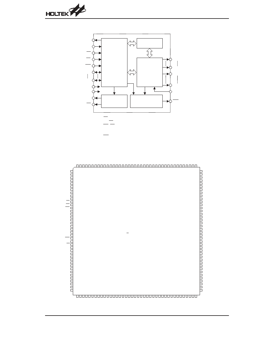
Block Diagram
Pin Assignment
HT1660
Rev. 1.00
2
September 16, 2003
W a t c h d o g T i m e r
&
T i m e B a s e G e n e r a t o r
D i s p l a y R A M
L C D D r i v e r /
B i a s C i r c u i t
C o n t r o l
&
T i m i n g
C i r c u i t
W R
O S C I
C S
R D
C O M 0
C O M 3 1
S E G 0
S E G 9 5
T o n e F r e q u e n c y
G e n e r a t o r
B Z
B Z
I R Q
V S S
V D D
V L C D
O S C O
D B 0
D B 3
N o t e : C S : C h i p s e l e c t i o n
B Z , B Z : T o n e o u t p u t s
W R , R D : W R I T E c l o c k , R E A D c l o c k
D B 0 ~ D B 3 : D a t a b u s
C O M 0 ~ C O M 3 1 , S E G 0 ~ S E G 9 5 : L C D o u t p u t s
I R Q : T i m e b a s e o r W D T o v e r f l o w o u t p u t
1
2
3
4
5
6
7
8
9
1 0
1 1
1 2
1 3
1 4
1 5
1 6
1 7
1 8
1 9
2 0
2 1
2 2
2 3
2 4
2 5
2 6
2 7
2 8
2 9
3 0
3 1
3 2
3 3
3 4
3 5
3 6
3 7
3 8
3 9
4 0
4 1
1 2 0
1 1 9
1 1 8
1 1 7
1 1 6
1 1 5
1 1 4
1 1 3
1 1 2
1 1 1
1 1 0
1 0 9
1 0 8
1 0 7
1 0 6
1 0 5
1 0 4
1 0 3
1 0 2
1 0 1
1 0 0
9 9
9 8
9 7
9 6
9 5
9 4
9 3
9 2
9 1
9 0
8 9
8 8
8 7
8 6
8 5
8 4
8 3
8 2
8 1
4 2 4 3 4 4 4 5 4 6 4 7 4 8 4 9 5 0 5 1 5 2 5 3 5 4 5 5 5 6 5 7 5 8 5 9 6 0 6 1 6 2 6 3 6 4 6 5 6 6 6 7 6 8 6 9 7 0 7 1 7 2 7 3 7 4 7 5 7 6 7 7 7 8 7 9 8 0
1 6 0 1 5 9 1 5 8 1 5 7 1 5 6 1 5 5 1 5 4 1 5 3 1 5 2 1 5 1 1 5 0 1 4 9 1 4 8 1 4 7 1 4 6 1 4 5 1 4 4 1 4 3 1 4 2 1 4 1 1 4 0 1 3 9 1 3 8 1 3 7 1 3 6 1 3 5 1 3 4 1 3 3 1 3 2 1 3 1 1 3 0 1 2 9 1 2 8 1 2 7 1 2 6 1 2 5 1 2 4 1 2 3 1 2 2 1 2 1
H T 1 6 6 0
1 6 0 Q F P - A
C O M 1 9
C O M 1 8
C O M 1 7
C O M 1 6
N C
N C
N C
N C
N C
N C
C S
R D
W R
D B 0
D B 1
D B 2
D B 3
V S S
O S C I
O S C O
V D D
V L C D
I R Q
B Z
B Z
T 1
T 2
T 3
T 4
T 0 0 0
V L C D
N C
N C
N C
N C
N C
C O M 0
C O M 1
C O M 2
C O M 3
S
E
G
2
7
S
E
G
2
6
S
E
G
2
5
S
E
G
2
4
S
E
G
2
3
S
E
G
2
2
S
E
G
2
1
S
E
G
2
0
S
E
G
1
9
S
E
G
1
8
S
E
G
1
7
S
E
G
1
6
S
E
G
1
5
S
E
G
1
4
S
E
G
1
3
S
E
G
1
2
S
E
G
1
1
S
E
G
1
0
S
E
G
9
S
E
G
8
S
E
G
7
S
E
G
6
S
E
G
5
S
E
G
4
S
E
G
3
S
E
G
2
S
E
G
1
S
E
G
0
C
O
M
1
5
C
O
M
1
4
C
O
M
1
3
C
O
M
1
2
C
O
M
1
1
C
O
M
1
0
C
O
M
9
C
O
M
8
C
O
M
7
C
O
M
6
C
O
M
5
C
O
M
4
S E G 6 7
S E G 6 6
S E G 6 5
S E G 6 4
S E G 6 3
S E G 6 2
S E G 6 1
S E G 6 0
S E G 5 9
S E G 5 8
S E G 5 7
S E G 5 6
S E G 5 5
S E G 5 4
S E G 5 3
S E G 5 2
S E G 5 1
S E G 5 0
S E G 4 9
S E G 4 8
S E G 4 7
S E G 4 6
S E G 4 5
S E G 4 4
S E G 4 3
S E G 4 2
S E G 4 1
S E G 4 0
S E G 3 9
S E G 3 8
S E G 3 7
S E G 3 6
S E G 3 5
S E G 3 4
S E G 3 3
S E G 3 2
S E G 3 1
S E G 3 0
S E G 2 9
S E G 2 8
S
E
G
6
8
S
E
G
6
9
S
E
G
7
0
S
E
G
7
1
S
E
G
7
2
S
E
G
7
3
S
E
G
7
4
S
E
G
7
5
S
E
G
7
6
S
E
G
7
7
S
E
G
7
8
S
E
G
7
9
S
E
G
8
0
S
E
G
8
1
S
E
G
8
2
S
E
G
8
3
S
E
G
8
4
S
E
G
8
5
S
E
G
8
6
S
E
G
8
7
S
E
G
8
8
S
E
G
8
9
S
E
G
9
0
S
E
G
9
1
S
E
G
9
2
S
E
G
9
3
S
E
G
9
4
S
E
G
9
5
C
O
M
3
1
C
O
M
3
0
C
O
M
2
9
C
O
M
2
8
C
O
M
2
7
C
O
M
2
6
C
O
M
2
5
C
O
M
2
4
C
O
M
2
3
C
O
M
2
2
C
O
M
2
1
C
O
M
2
0
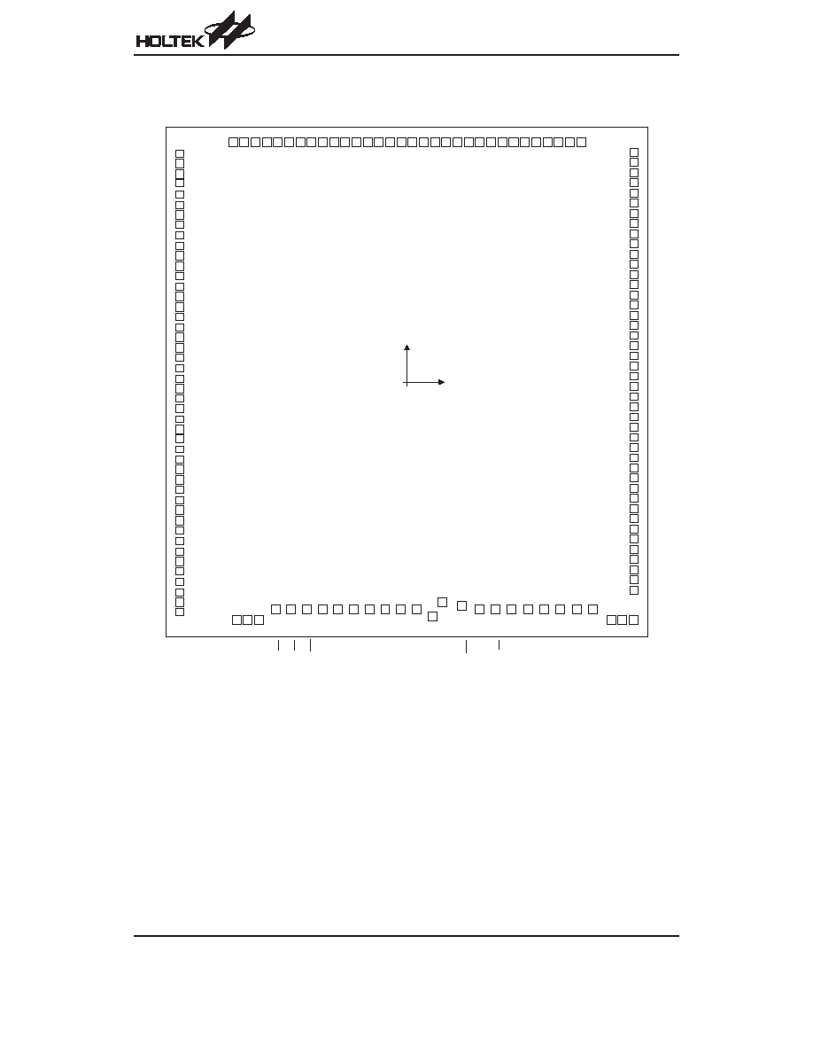
Pad Assignment
Chip size: 4340
´5030 (mm)
2
* The IC substrate should be connected to VSS in the PCB layout artwork.
HT1660
Rev. 1.00
3
September 16, 2003
( 0 , 0 )
1
2
3
4
5
6
7
8
9
1 0
1 1
1 2
1 3
1 4
1 5
1 6
1 7
1 8
1 9
2 0
2 1
2 2
2 3
2 4
2 5
2 6
2 7
2 8
2 9
3 0
3 1
3 2
3 3
3 4
3 5
3 6
3 7
3 8
3 9
4 0
4 1
4 2
4 3
4 4
4 5
4 6
4 7 4 8 4 9
5 0
5 1
5 2
5 3
5 4
5 5
5 6
5 7
5 8
5 9
6 0
6 1
6 2
6 3
6 4
6 5
6 6
6 7
6 8
6 9
7 0
7 1 7 2 7 3
7 4
7 5
1 1 7
1 1 6
1 1 5
1 1 4
1 1 3
1 1 2
1 1 1
1 1 0
1 0 9
1 0 8
1 0 7
1 0 6
1 0 5
1 0 4
1 0 3
1 0 2
1 0 1
1 0 0
9 9
9 8
9 7
9 6
9 5
9 4
9 3
9 2
9 1
9 0
8 9
8 8
8 7
8 6
8 5
8 4
8 3
8 2
8 1
8 0
7 9
7 8
7 7
7 6
1 1 8
1 1 9
1 2 0
1 2 1
1 2 2
1 2 3
1 2 4
1 2 5
1 2 6
1 2 7
1 2 8
1 2 9
1 3 0
1 3 1
1 3 2
1 3 3
1 3 4
1 3 5
1 3 6
1 3 7
1 3 8
1 3 9
1 4 0
1 4 1
1 4 2
1 4 3
1 4 4
1 4 5
1 4 6
1 4 7
1 4 8
1 4 9
S E G 6 3
S E G 6 4
S E G 6 5
S E G 6 6
S E G 6 7
S E G 6 8
S E G 6 9
S E G 7 0
S E G 7 1
S E G 7 2
S E G 7 3
S E G 7 4
S E G 7 5
S E G 7 6
S E G 7 7
S E G 7 8
S E G 7 9
S E G 8 0
S E G 8 1
S E G 8 2
S E G 8 3
S E G 8 4
S E G 8 5
S E G 8 6
S E G 8 7
S E G 8 8
S E G 8 9
S E G 9 0
S E G 9 1
S E G 9 2
S E G 9 3
S E G 9 4
S E G 9 5
C O M 3 1
C O M 3 0
C O M 2 9
C O M 2 8
C O M 2 7
C O M 2 6
C O M 2 5
C O M 2 4
C O M 2 3
C O M 2 2
C O M 2 1
C O M 2 0
C O M 1 9
C
O
M
1
8
C
O
M
1
7
C
O
M
1
6
C
O
M
2
C
O
M
1
C
O
M
0
V
L
C
D
T
4
T
3
T
2
T
1
B
Z
B
Z
I
R
Q
V
L
C
D
V
D
D
O
S
C
O
O
S
C
I
V
S
S
D
B
3
D
B
2
D
B
1
D
B
0
W
R
R
D
C
S
T
0
0
0
S E G 3 0
S E G 2 9
S E G 2 8
S E G 2 7
S E G 2 6
S E G 2 5
S E G 2 4
S E G 2 3
S E G 2 2
S E G 2 1
S E G 2 0
S E G 1 9
S E G 1 8
S E G 1 7
S E G 1 6
S E G 1 5
S E G 1 4
S E G 1 3
S E G 1 2
S E G 1 1
S E G 1 0
S E G 9
S E G 8
S E G 7
S E G 6
S E G 5
S E G 4
S E G 3
S E G 2
S E G 1
S E G 0
C O M 1 5
C O M 1 4
C O M 1 3
C O M 1 2
C O M 1 1
C O M 1 0
C O M 9
C O M 8
C O M 7
C O M 6
C O M 5
C O M 4
C O M 3
S
E
G
3
1
S
E
G
3
2
S
E
G
3
3
S
E
G
3
4
S
E
G
3
5
S
E
G
3
6
S
E
G
3
7
S
E
G
3
8
S
E
G
3
9
S
E
G
4
0
S
E
G
4
1
S
E
G
4
2
S
E
G
4
3
S
E
G
4
4
S
E
G
4
5
S
E
G
4
6
S
E
G
4
7
S
E
G
4
8
S
E
G
4
9
S
E
G
5
0
S
E
G
5
1
S
E
G
5
2
S
E
G
5
3
S
E
G
5
4
S
E
G
5
5
S
E
G
5
6
S
E
G
5
7
S
E
G
5
8
S
E
G
5
9
S
E
G
6
0
S
E
G
6
1
S
E
G
6
2
Pad Coordinates
Unit:
mm
Pad No.
X
Y
Pad No.
X
Y
Pad No.
X
Y
1
-2028.50
2237.20
51
-1027.85
-2225.20
101
2028.45
654.20
2
-2028.50
2137.20
52
-892.45
-2225.20
102
2028.45
754.20
3
-2028.50
2037.20
53
-745.55
-2225.20
103
2028.45
854.20
4
-2028.50
1937.20
54
-610.15
-2225.20
104
2028.45
954.20
5
-2028.50
1837.20
55
-464.85
-2225.20
105
2028.45
1054.20
6
-2028.50
1637.20
56
-329.25
-2225.20
106
2028.45
1154.20
7
-2028.50
1537.20
57
-187.15
-2225.30
107
2028.45
1254.20
8
-2028.50
1437.20
58
-53.65
-2229.70
108
2028.45
1354.20
9
-2028.50
1337.20
59
84.55
-2229.70
109
2028.45
1454.20
10
-2028.50
1237.20
60
222.85
-2297.35
110
2028.45
1554.20
11
-2028.50
1237.20
61
310.40
-2162.35
111
2028.45
1654.20
12
-2028.50
1137.20
62
492.00
-2183.60
112
2028.45
1754.20
13
-2028.50
1037.20
63
638.50
-2225.30
113
2028.45
1854.20
14
-2028.50
937.20
64
773.90
-2225.30
114
2028.45
1954.20
15
-2028.50
837.20
65
933.50
-2225.30
115
2028.45
2054.20
16
-2028.50
737.20
66
1081.70
-2225.30
116
2028.45
2154.20
17
-2028.50
637.20
67
1228.70
-2225.30
117
2028.45
2254.20
18
-2028.50
537.20
68
1376.90
-2225.30
118
1550.75
2349.60
19
-2028.50
437.20
69
1523.90
-2225.30
119
1450.75
2349.60
20
-2028.50
337.20
70
1662.50
-2225.30
120
1350.75
2349.60
21
-2028.50
237.20
71
1821.19
-2338.90
121
1250.75
2349.60
22
-2028.50
137.20
72
1921.19
-2338.90
122
1150.75
2349.60
23
-2028.50
37.20
73
2021.19
-2338.90
123
1050.75
2349.60
24
-2028.50
-62.80
74
2028.45
-2051.10
124
950.75
2349.60
25
-2028.50
-162.80
75
2028.45
-1951.10
125
850.75
2349.60
26
-2028.50
-262.80
76
2028.45
-1851.10
126
750.75
2349.60
27
-2028.50
-362.80
77
2028.45
-1751.10
127
650.75
2349.60
28
-2028.50
-462.80
78
2028.45
-1651.10
128
550.75
2349.60
29
-2028.50
-562.80
79
2028.45
-1551.10
129
450.75
2349.60
30
-2028.50
-662.80
80
2028.45
-1451.10
130
350.75
2349.60
31
-2028.50
-762.80
81
2028.45
-1351.10
131
250.75
2349.60
32
-2028.50
-862.80
82
2028.45
-1251.10
132
150.75
2349.60
33
-2028.50
-962.80
83
2028.45
-1151.10
133
50.75
2349.60
34
-2028.50
-1062.80
84
2028.45
-1051.10
134
-49.25
2349.60
35
-2028.50
-1162.80
85
2028.45
-951.10
135
-149.25
2349.60
36
-2028.50
-1262.80
86
2028.45
-851.10
136
-249.25
2349.60
37
-2028.50
-1362.80
87
2028.45
-745.80
137
-349.25
2349.60
38
-2028.50V -1462.80
88
2028.45
-645.80
138
-449.25
2349.60
39
-2028.50
-1562.80
89
2028.45
-545.80
139
-549.25
2349.60
40
-2028.50
-1662.80
90
2028.45
-445.80
140
-649.25
2349.60
41
-2028.50
-1762.80
91
2028.45
-345.80
141
-749.25
2349.60
42
-2028.50
-1862.80
92
2028.45
-245.80
142
-849.25
2349.60
43
-2028.50
-1962.80
93
2028.45
-145.80
143
-949.25
2349.60
44
-2028.50
-2062.80
94
2028.45
-45.80
144
-1049.25
2349.60
45
-2028.50
-2162.80
95
2028.45
54.20
145
-1149.25
2349.60
46
-2028.50
-2262.80
96
2028.45
154.20
146
-1249.25
2349.60
47
-1523.55
-2337.10
97
2028.45
254.20
147
-1349.25
2349.60
48
-1423.55
-2337.10
98
2028.45
354.20
148
-1449.25
2349.60
49
-1323.55
-2337.10
99
2028.45
454.20
149
-1549.25
2349.60
50
-1170.45
-2225.20
100
2028.45
554.20
HT1660
Rev. 1.00
4
September 16, 2003
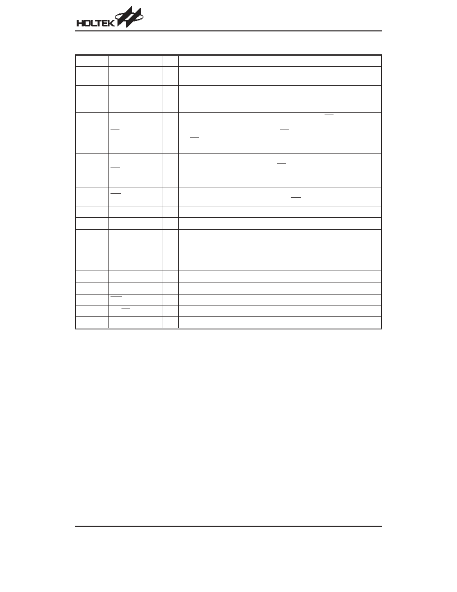
Pad Description
Pad No.
Pad Name
I/O
Description
1~33
87~149
SEG63~SEG95
SEG0~SEG62
O
LCD segment outputs
34~49
71~86
COM31~COM16
COM0~COM15
O
LCD common outputs, under 112
´16 command mode, COM16~COM31 will
share to SEG96~SEG111. COM31/SEG96, COM30/SEG97, COM29/
SEG98....., COM18/SEG109, COM17/SEG110, COM16/SEG111
50
CS
I
Chip selection input with pull-high resistor. When the CS is logic high, the
data and command read from or write to the HT1660 are disabled. The serial
interface circuit is also reset. But if the CS is at a logic low level and is input to
the CS pad, the data and command transmission between the host controller
and the HT1660 are all enabled.
51
RD
I
READ clock input with pull-high resistor. Data in the RAM of the HT1660 are
clocked out on the falling edge of the RD signal. The clocked out data will ap-
pear on the data line. The host controller can use the next rising edge to latch
the clocked out data.
52
WR
I
WRITE clock input with pull-high resistor. Data on the DATA line are latched
into the HT1660 on the rising edge of the WR signal.
53~56
DB0~DB3
I/O
Parallel data input/output with a pull-high resistor
57
VSS
¾ Negative power supply for logic circuit, ground
58
59
OSCI
OSCO
I
O
The OSCI and OSCO pads are connected to a 32.768kHz crystal in order to
generate a system clock. If the system clock comes from an external clock
source, the external clock source should be connected to the OSCI pad. But
if an on-chip RC oscillator is selected, the OSCI and OSCO pads can be left
open.
60
VDD
¾ Positive power supply for logic circuit
61
VLCD
I
Power supply for LCD driver circuit
62
IRQ
O
Time base or Watchdog Timer overflow flag, NMOS open drain output.
63, 64
BZ, BZ
O
2kHz or 4kHz frequency output pair (tristate output buffer)
65~69
T1~T4, T000
I
Not connected
Absolute Maximum Ratings
Supply Voltage ...........................V
SS
-0.3V to V
SS
+5.5V
Storage Temperature ............................
-50°C to 125°C
Input Voltage.............................V
SS
-0.3V to V
DD
+0.3V
Operating Temperature...........................
-25°C to 75°C
Note: These are stress ratings only. Stresses exceeding the range specified under
²Absolute Maximum Ratings² may
cause substantial damage to the device. Functional operation of this device at other conditions beyond those
listed in the specification is not implied and prolonged exposure to extreme conditions may affect device reliabil-
ity.
HT1660
Rev. 1.00
5
September 16, 2003
Document Outline
- þÿ
- þÿ
- þÿ
- þÿ
- þÿ
- þÿ
- þÿ
- þÿ
- þÿ
- þÿ
- þÿ
- þÿ
- þÿ
- þÿ
- þÿ
- þÿ