 | ÐлекÑÑоннÑй компоненÑ: HT23C010 | СкаÑаÑÑ:  PDF PDF  ZIP ZIP |
Äîêóìåíòàöèÿ è îïèñàíèÿ www.docs.chipfind.ru
HT23C010
CMOS 128K
×
8-Bit Mask ROM
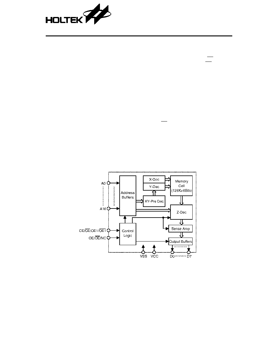
Block Diagram
Features
·
Operating voltage: 2.7V~5.5V
·
Low power consumption
Operation: 25mA Max. (V
CC
=5V)
10mA Max. (V
CC
=3V)
Standby: 30
µ
A Max. (V
CC
=5V)
10
µ
A Max. (V
CC
=3V)
·
Access time:150ns Max. (V
CC
=5V)
250ns Max. (V
CC
=3V)
·
131072
×
8 bits of mask ROM
·
Mask options: chip enable CE/CE/OE1/
OE1B and output enable OE/OE/NC
·
TTL compatible inputs and outputs
·
Tristate outputs
·
Fully static operation
·
Package type: 28-pin DIP/SOP
32-pin DIP/SOP/PLCC
General Description
The HT23C010 is a read-only memory with
high performance CMOS storage device whose
1024K of memory is arranged into 131072
words by 8 bits.
For application flexibility, the chip enable and
output enable control pins can be selected as
active high or active low. This flexibility not
only allows easy interface with most microproc-
essors, but also eliminates bus contention in
multiple bus microprocessor systems. An addi-
tional feature of the HT23C010 is its ability to
enter the standby mode whenever the chip en-
able (CE/CE) is inactive, thus reducing current
consumption to below 30
µ
A. The combination of
these functions makes the chip suitable for high
density low power memory applications.
1
24th Aug '98
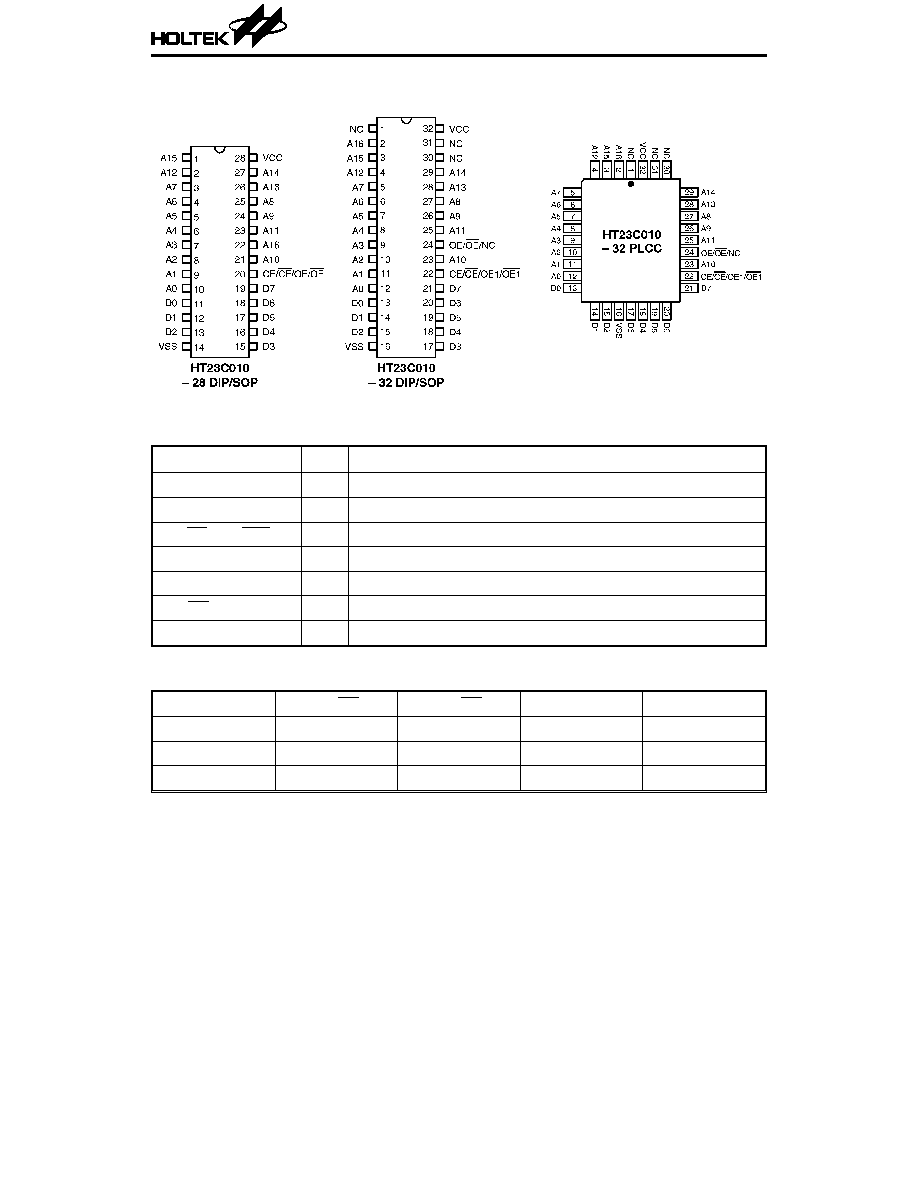
Pin Assignment
Pin Description
Pin Name
I/O
Description
A0~A16
I
Address inputs
D0~D7
O
Data outputs
CE/CE/OE1/OE1
I
Chip enable output enable input
VSS
I
Negative power supply
VCC
I
Positive power supply
OE/OE/NC
I
Output enable input
NC
--
No connection
Operation Truth Table
Mode
CE/CE
OE/OE
A0~A16
D0~D7
Read
H/L
H/L
Valid
Data Out
Deselect
H/L
L/H
X
High Z
Standby
L/H
X
X
High Z
Note: H=V
IH
, L=V
IL
, X=V
IH
or V
IL
HT23C010
2
24th Aug '98
Absolute Maximum Ratings*
Supply Voltage ................................. 0.3V to 6V
Storage Temperature................. 50
°
C to 125
°
C
Input Voltage........................ 0.3V to V
CC
+0.3V
Operating Temperature............... 40
°
C to 85
°
C
*Note: These are stress ratings only. Stresses exceeding the range specified under "Absolute Maxi-
mum Ratings" may cause substantial damage to the device. Functional operation of this
device at other conditions beyond those listed in the specification is not implied and prolonged
exposure to extreme conditions may affect device reliability.
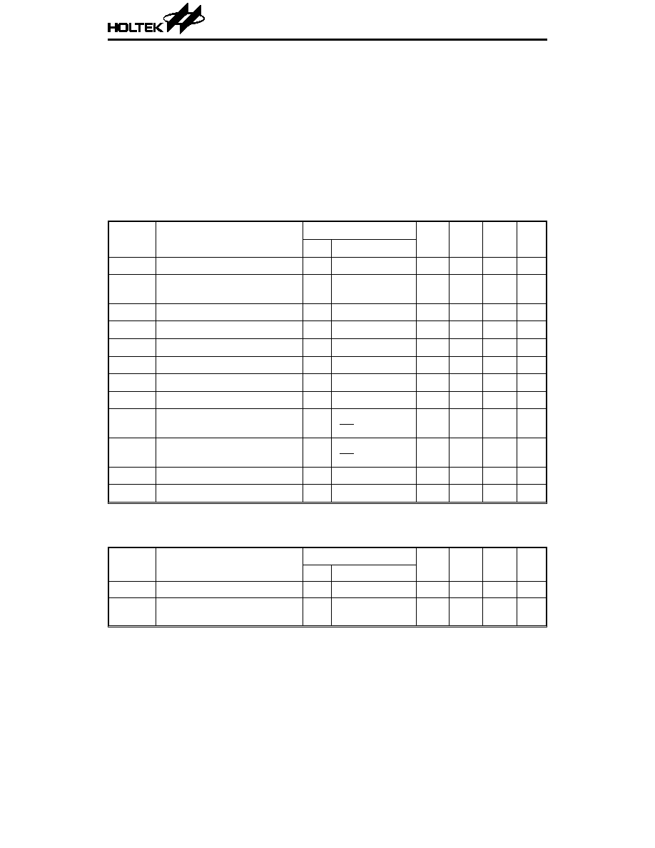
D.C. Characteristics
Supply voltage: 2.7V~3.6V
Ta=40
°
C to 85
°
C
Symbol
Parameter
Test Conditions
Min.
Typ.
Max. Unit
V
CC
Conditions
V
CC
Operating Voltage
--
--
2.7
--
3.6
V
I
CC
Operating Current
3V
O/P Unload,
f=5MHz
--
--
10
mA
V
IL
Input Low Voltage
3V
--
V
SS
--
0.4
V
V
IH
Input High Voltage
3V
--
2.0
--
V
CC
V
V
OL
Output Low Voltage
3V
I
OL
=2.1mA
--
--
0.4
V
V
OH
Output High Voltage
3V
I
OH
=0.4mA
2.4
--
V
CC
V
I
LI
Input Leakage Current
3V
V
IN
=0 to V
CC
--
--
10
µ
A
I
LO
Output Leakage Current
3V
V
OUT
=0 to V
CC
--
--
10
µ
A
I
STB1
Standby Current
3V
CE=V
IL
CE=V
IH
--
--
500
µ
A
I
STB2
Standby Current
3V
CE
0.2V
CE
V
CC
-0.2V
--
--
10
µ
A
C
IN
Input Capacitance (See note)
--
f=1MHz
--
--
10
pF
C
OUT
Output Capacitance (See note)
--
f=1MHz
--
--
10
pF
Note: These parameters are periodically sampled but not 100% tested.
Supply voltage: 4.5V~5.5V
Ta=40
°
C to 85
°
C
Symbol
Parameter
Test Conditions
Min.
Typ.
Max. Unit
V
CC
Conditions
V
CC
Operating Voltage
--
--
4.5
--
5.5
V
I
CC
Operating Current
5V
O/P Unload,
f=5MHz
--
--
25
mA
HT23C010
3
24th Aug '98
Symbol
Parameter
Test Conditions
Min.
Typ.
Max. Unit
V
CC
Conditions
V
IL
Input Low Voltage
5V
--
V
SS
--
0.8
V
V
IH
Input High Voltage
5V
--
2.2
--
V
CC
V
V
OL
Output Low Voltage
5V
I
OL
=3.2mA
--
--
0.4
V
V
OH
Output High Voltage
5V
I
OH
=1mA
2.4
--
V
CC
V
I
LI
Input Leakage Current
5V
V
IN
=0 to V
CC
--
--
10
µ
A
I
LO
Output Leakage Current
5V
V
OUT
=0 to V
CC
--
--
10
µ
A
I
STB1
Standby Current
5V
CE=V
IL
CE=V
IH
--
--
1.5
mA
I
STB2
Standby Current
5V
CE
0.2V
CE
V
CC
-0.2V
--
--
30
µ
A
C
IN
Input Capacitance (See note)
--
f=1MHz
--
--
10
pF
C
OUT
Output Capacitance (See note)
--
f=1MHz
--
--
10
pF
Note: These parameters are periodically sampled but not 100% tested.
A.C. Characteristics
Ta=40
°
C to 85
°
C
Symbol
Parameter
V
CC
=2.7V~3.6V
V
CC
=4.5V~5.5V
Unit
Min.
Max.
Min.
Max.
t
CYC
Cycle Time
250
--
150
--
ns
t
AA
Address Access Time
--
250
--
150
ns
t
ACE
Chip Enable Access Time
--
250
--
150
ns
t
AOE
Output Enable Access Time
--
150
--
80
ns
t
OH
Output Hold Time
--
--
10
--
ns
t
OD
Output Disable Time (See Note)
--
--
--
70
ns
t
OE
Output Enable Time (See Note)
--
--
10
--
ns
Note: These parameters are periodically sampled but not 100% tested.
A.C. test conditions
Output load: see figure right
Input rise and fall time: 10ns
Input pulse levels: 0.4V to 2.4V (V
CC
=5V)
Input and output timing reference levels:
0.8V and 2.0V (V
CC
=5V)
1.5V (V
CC
=3V)
Output load circuit
HT23C010
4
24th Aug '98
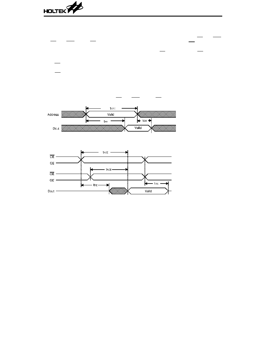
Timing Diagrams
·
Propagation delay due to address (CE/CE/OE1/OE1 and OE/OE are active)
·
Propagation delay due to chip and output enable (address valid)
Functional Description
The HT23C010 has two modes, namely data
read mode and standby mode, controlled by
CE/CE/OE1/OE1 and OE/OE/NC inputs.
·
Standby mode
The HT23C010 offers lower current consump-
tion, controlled by the chip enable input
(CE/CE). When a low/high level is applied to the
CE/CEB input regardless of the output enable
(OE/OE/NC) states the chip will enter the
standby mode.
·
Data read mode
When both the chip enable (CE/CE/OE1/OE1)
and the output enable (OE/OE/NC) are active,
the chip is in data read mode. Otherwise,
active CE/CE and inactive OE/OE/NC result
in deselect mode. The output will remain in
Hi-Z state.
HT23C010
5
24th Aug '98
Document Outline