 | ÐлекÑÑоннÑй компоненÑ: HT25LC512 | СкаÑаÑÑ:  PDF PDF  ZIP ZIP |
Äîêóìåíòàöèÿ è îïèñàíèÿ www.docs.chipfind.ru
HT25LC512
CMOS 64K´8-Bit SPI Serial OTP EPROM
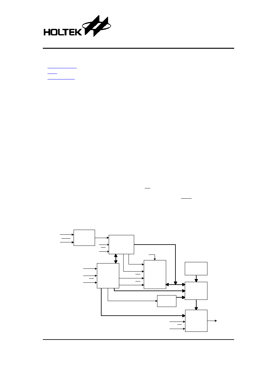
Block Diagram
Rev. 1.10
1
October 17, 2005
Features
·
Operating voltage: 2.7V~3.6V
·
Programming voltage
-
V
PP
=12.5V
±0.2V
-
V
CC
=6.0V
±0.2V
·
512K-bit OTP ROM, access command compatible
with AT25F512
·
64K
´8-bit organization
·
12MHz max. clock frequency @VCC=2.7V
15MHz max. clock frequency @VCC=3.0V
·
Serial interface architecture
·
Serial Peripheral Interface (SPI) compatible - modes
0 and 3
·
CMOS and TTL compatible inputs and outputs
·
Pin assignment compatible with AT25F512
·
Commercial temperature range (0
°C to +70°C)
·
8-pin SOP package
General Description
The HT25LC512 is a 512K-bit OTP ROM of which func-
tion and pin assignment are compatible with AT25F512
and can directly replace the AT25F512 for cost down
purposes when the memory in the system is just read
only. There are 512K bits of memory which are orga-
nized as 65536 words of 8 bits each. The HT25LC512
uses a serial interface to sequentially access its data.
The simple serial interface facilitates hardware layout,
increase system reliability, minimize switching noise,
and reduce package size and active pin count. The de-
vice is optimized for use in many commercial and indus-
trial applications where high density, low pin count, low
voltage, and low power consumption are essential. The
device operates at clock frequencies up to 10MHZ.
The HT25LC512 is enabled through the chip select pin
(CS) and accessed via a three-wire interface consisting
of the Serial Input (SI), Serial Output (SO), and the Se-
rial Clock (SCK). The HOLD pin may be used to sus-
pend any serial communication without resetting the
serial sequence.
X - a d d r
Y - a d d r
C E
O E
V P P
O T P R O M
S t a t e
C o n t r o l
I D
R e g i s t e r
P I S O
R e g i s t e r
S C L K
C S
S O
O u t p u t
M U X
S t a t u s
R e g i s t e r
S I P O
R e g i s t e r
C S
S I
S C L K
C S
S I
S C L K
C l o c k
G e n e r a t o r
S C K
H O L D
Technical Document
·
Tools Information
·
FAQs
·
Application Note
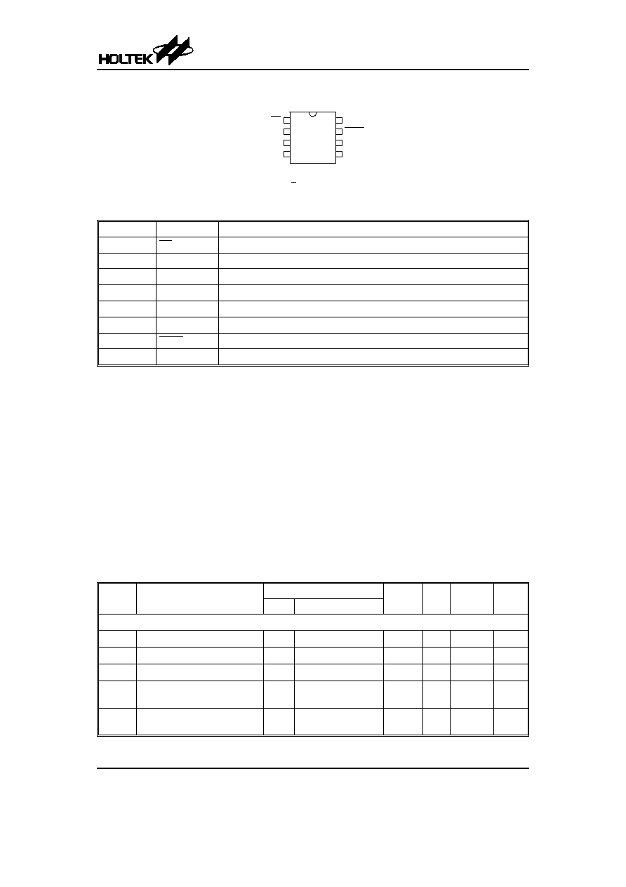
Pin Assignment
Pin Description
Pin No.
Pin Name
Description
1
CS
Chip select
2
SO
Serial Output
3
VPP
Program voltage supply
4
GND
Negative power supply, ground
5
SI
Serial input
6
SCK
Serial clock
7
HOLD
Suspends serial input
8
VCC
Positive power supply
Absolute Maximum Rating
Operation Temperature Commercial ..........................................................................................................0
°C to +70°C
Storage Temperature.............................................................................................................................
-65°C to 125 °C
Applied VCC Voltage with Respect to VSS ................................................................................................
-0.6V to 7.0V
Applied Voltage on Input Pin with Respect to VSS .....................................................................................
-0.6V to 7.0V
Applied Voltage on Output Pin with Respect to VSS .........................................................................
-0.6V to V
CC
+0.5V
Applied VPP Voltage with Respect to VSS...............................................................................................
-0.6V to 13.5V
Note: These are stress ratings only. Stresses exceeding the range specified under
²Absolute Maximum Ratings² may
cause substantial damage to the device. Functional operation of this device at other conditions beyond those
listed in the specification is not implied and prolonged exposure to extreme conditions may affect device reliabil-
ity.
D.C. Characteristics
Ta=0
°C to +70°C
Symbol
Parameter
Test Conditions
Min.
Typ.
Max.
Unit
V
CC
Conditions
Read Operation
V
CC
Supply Voltage
¾
¾
2.7
¾
3.6
V
V
IL
Input Low Voltage
¾
¾
-0.5
¾
0.2V
CC
V
V
IH
Input High Voltage
¾
¾
0.7V
CC
¾
V
CC
+0.5
V
V
OL
Output Low Voltage
2.7V~
3.6V
I
OL
=0.15mA;
2.7V
£ V
CC
£ 3.6V
¾
¾
0.2
V
V
OH
Output High Voltage
2.7V~
3.6V
I
OH
=
-100mA
V
CC
-0.2
¾
¾
V
HT25LC512
Rev. 1.10
2
October 17, 2005
1
2
3
4
8
7
6
5
C S
S O
V P P
G N D
V C C
H O L D
S C K
S I
H T 2 5 L C 5 1 2
8 S O P - A
Symbol
Parameter
Test Conditions
Min.
Typ.
Max.
Unit
V
CC
Conditions
I
STB
Standby Current
2.7V~
3.6V
CS=V
CC
=3.6V, all in-
puts at CMOS levels
¾
2
10
mA
I
CC
Active Current, Read Operation
2.7V~
3.6V
f=10MHz; SO=open
V
CC
=3.6V
¾
10
15
mA
I
IL
Input Leakage Current
2.7V~
3.6V
V
IN
=0V to V
CC
-3
¾
3
mA
I
OL
Output Leakage Current
2.7V~
3.6V
V
IN
=0V to V
CC
-3
¾
3
mA
Programming Operation
V
CC
Supply Voltage
¾
¾
5.8
6.0
6.2
V
V
PP
Supply Voltage
¾
¾
12.3
12.5
12.7
V
V
IL
Input Low Voltage
6.0V
¾
-0.5
¾
0.2V
CC
V
V
IH
Input High Voltage
6.0V
¾
0.7V
CC
¾
V
CC
+0.5
V
I
CC
V
CC
Supply current
6.0V
¾
¾
¾
40
mA
I
PP
V
PP
Supply Current
6.0V
¾
¾
¾
10
mA
Note:
V
PP
overshoot/undershoot riaging caused by fast rising time must not go below 11V or above 13V.
A.C. Characteristics
Ta=0
°C to +70°C, V
CC
=2.7V to 3.6V
Symbol
Parameter
Test Conditions
Min.
Typ.
Max.
Unit
f
SCK
SCK Frequency
V
CC
=2.7V~3.0V
0
¾
12
MHz
V
CC
=3.0V~3.6V
0
¾
15
MHz
t
WH
SCK High Time
V
CC
=2.7V~3.0V
36
¾
¾
ns
V
CC
=3.0V~3.6V
28
¾
¾
ns
t
WL
SCK Low Time
V
CC
=2.7V~3.0V
36
¾
¾
ns
V
CC
=3.0V~3.6V
28
¾
¾
ns
t
CS
Minimum CS High Time
V
CC
=2.7V~3.6V
25
¾
¾
ns
t
CSS
CS Setup Time
V
CC
=2.7V~3.6V
25
¾
¾
ns
t
CSH
CS Hold Time
V
CC
=2.7V~3.6V
25
¾
¾
ns
t
SU
Data in Setup Time
V
CC
=2.7V~3.6V
20
¾
¾
ns
t
H
Data in Hold Time
V
CC
=2.7V~3.6V
5
¾
¾
ns
t
CD
HOLD Setup Time
V
CC
=2.7V~3.6V
20
¾
¾
ns
t
HD
HOLD Hold Time
V
CC
=2.7V~3.6V
15
¾
¾
ns
t
HO
Output Hold Time
V
CC
=2.7V~3.6V
0
¾
¾
ns
t
DIS
Output Disable Time
V
CC
=2.7V~3.6V
¾
¾
100
ns
t
V
Output Valid
V
CC
=2.7V~3.0V
¾
¾
36
ns
V
CC
=3.0V~3.6V
¾
¾
28
ns
t
LZ
HOLD to Output Low Z
V
CC
=2.7V~3.6V
¾
¾
200
ms
t
HZ
HOLD to Output High Z
V
CC
=2.7V~3.6V
¾
¾
200
ms
HT25LC512
Rev. 1.10
3
October 17, 2005
Symbol
Parameter
Test Conditions
Min.
Typ.
Max.
Unit
Programming the OTP ROM
f
SCK
SCK Frequency
48
70
160
kHz
t
WH
SCK High Time
3
7.5
10.5
ms
t
WL
SCK Low Time
3
7.5
10.5
ms
t
CS
Minimum CS High Time
2
¾
¾
ms
t
CSS
CS Setup Time
2
¾
¾
ms
t
CSH
CS Hold Time
2
¾
¾
ms
t
SU
Data in Setup Time
100
¾
¾
ns
t
H
Data in Hold Time
100
¾
¾
ns
Note:
For normal READ operation, don
¢t use the 99H instruction.
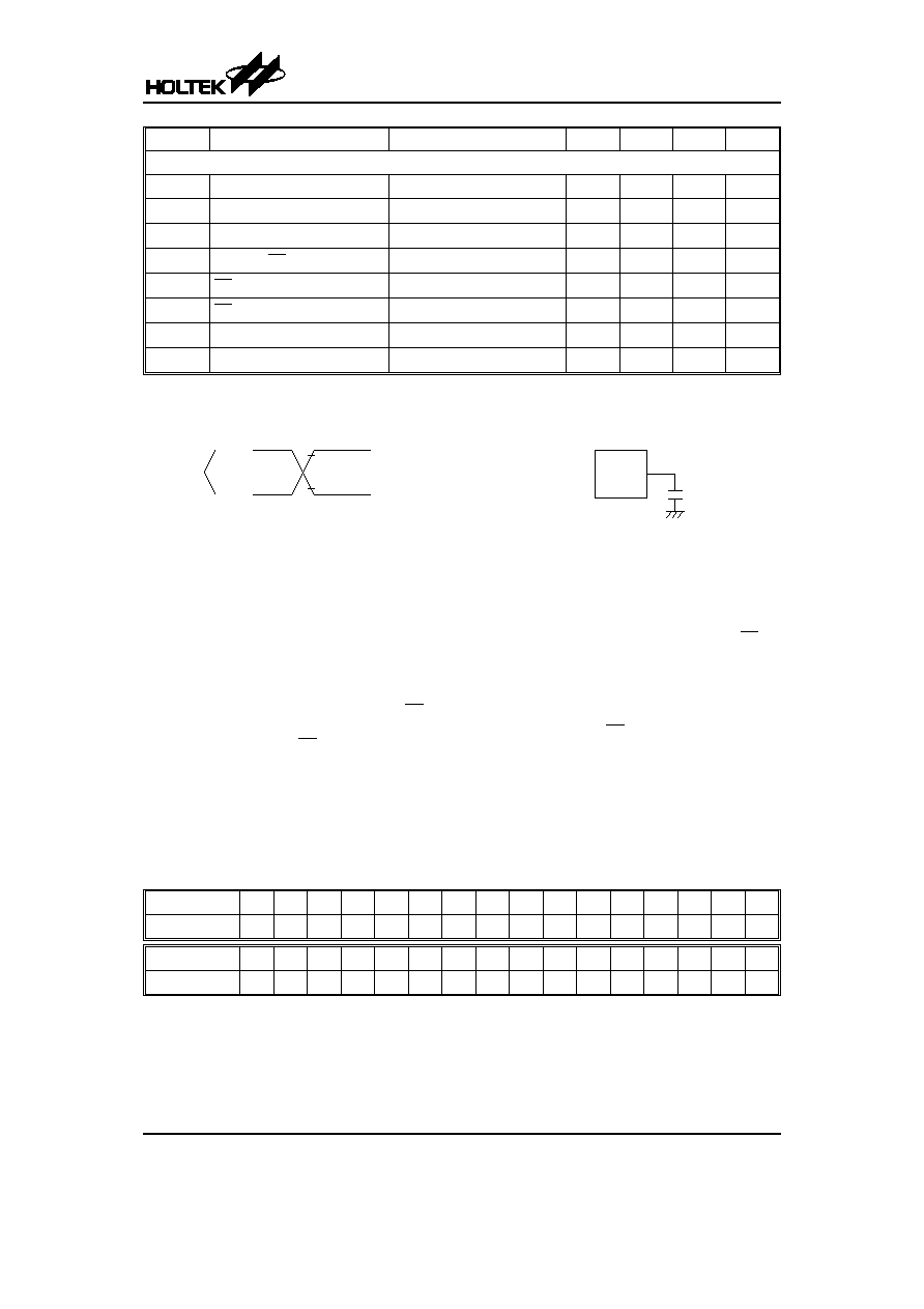
Test Waveforms and Measurements
Output Test Load
HT25LC512
Rev. 1.10
4
October 17, 2005
Functional Description
Device Operation
The HT25LC512 operation is controlled by instructions
from the host processor. The HT25LC512 has only 3
kinds of instructions, Memory Read, Status Register
read and Product ID Read. Any invalid instruction will
be ignored without response from the HT25LC512. A
valid instruction starts with the falling edge of CS fol-
lowed by the appropriate 8-bit opcode and the memory
address location. While the CS pin is low, toggling the
SCK pin controls the loading of the opcode and the
memory address location through the SI (serial input)
pin. All instructions, addresses and data are transferred
with the most significant bit (MSB) first.
·
Memory read
Reading the HT25LC512 via the SO (Serial Output)
pin requires the following sequence. After the CS line
is pulled low to select a device, the READ instruction
is transmitted via the SI line followed by the byte ad-
dress to read. Upon completion, any data on the SI
line will be ignored. The data (D7-D0) at the specified
address is then shifted out onto the SO line. If only one
byte is to be read, the CS line should be driven high af-
ter the data comes out. The READ instruction can be
continued since the byte address is automatically in-
cremented and data will continue to be shifted out.
When the highest address is reached, the address
counter will roll over to the lowest address allowing the
entire memory to be read in one continuous READ in-
struction.
2 . 4 V
0 . 4 5 V
A C
M e a s u r e m e n t
L e v e l
A C D r i v i n g
L e v e l s
2 . 0 V
0 . 8 V
t
R
, t
F
< 5ns (10% to 90%)
D e v i c e
U n d e r
T e s t
3 0 p F
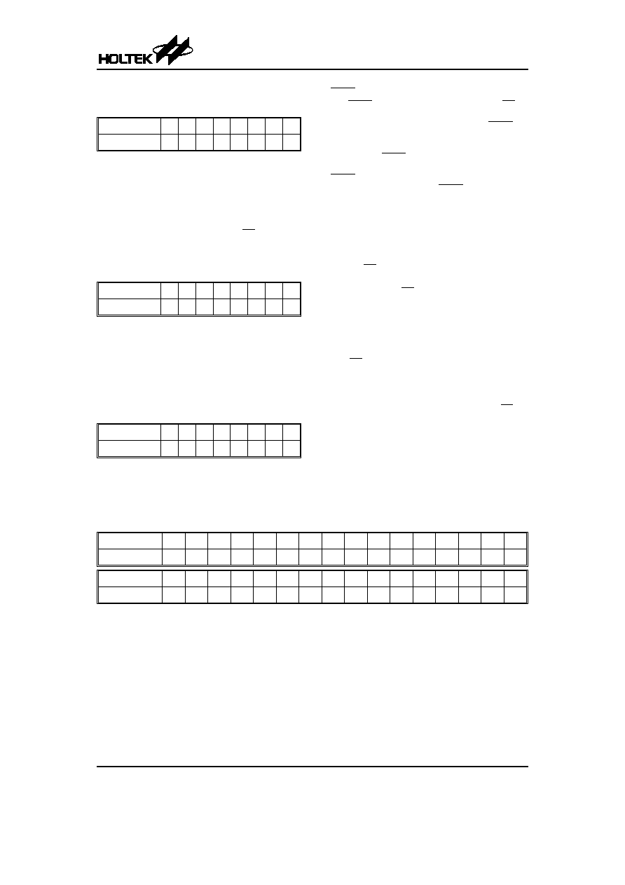
Memory read, bit sequence is shown as follows:
Bit Sequential
0
1
2
3
4
5
6
7
8
9
10
11
12
13
14
15
Bit data
0
0
0
0
x
0
1
1
x
x
x
x
x
x
x
0
Bit Sequential
16
17
18
19
20
21
22
23
24
25
26
27
28
29
30
31
Bit data
A15
A14
A13
A12
A11
A10
A9
A8
A7
A6
A5
A4
A3
A2
A1
A0
Note:
²x² don¢t care
HT25LC512
Rev. 1.10
5
October 17, 2005
·
Status register read
¨
Status register format
Bit Sequential
0
1
2
3
4
5
6
7
Bit Data
0
0
1
1
0
0
0
1
The data in the status register will always be 8CH.
To read the status register, the bit sequence is
shown below. After the last bit of the opcode is
shifted in, the eight bits of the status register, start-
ing with the MSB (bit 7), will be shifted out on the SO
pin during the next eight clock cycles. After bit 0 of
the status register has been shifted out, the se-
quence will repeat itself (as long as CS remains low
and SCK is being toggled) starting again with bit 7.
¨
Status register read
Bit sequence is shown as follows:
Bit Sequential
0
1
2
3
4
5
6
7
Bit Data
0
0
0
0
x
1
0
1
Note:
²x² don¢t care
·
Product ID read
The RDID instruction allows the user to read the man-
ufacturer and product ID of the device. The first byte
after the instruction will be the manufacture code
(1CH= HOLTEK), followed by the device code (83H
for 512K OTP ROM).
Product ID read, bit sequence is shown as follows:
Bit Sequential
0
1
2
3
4
5
6
7
Bit Data
0
0
0
1
x
1
0
1
Note: x: don
¢t care
·
HOLD
The HOLD pin is used in conjunction with the CS pin
to select the HT25LC512. When the device is se-
lected and a serial sequence is underway, HOLD can
be used to pause the serial communication with the
master device without resetting the serial sequence.
To pause, the HOLD pin must be brought low while the
SCK pin is low. To resume serial communication, the
HOLD pin is brought high while the SCK pin is low
(SCK may still toggle during HOLD). Inputs to the SI
pin will be ignored while the SO pin is in the high im-
pedance state.
Power-on State
When power is first applied to the device, the SO pin will
be in a high-impedance state, and a high-to-low transi-
tion on the CS pin will be required to start a valid instruc-
tion. The SPI mode will be automatically selected on
every falling edge of CS by sampling the inactive clock
state.
Programming the OTP ROM
Programming the OTP ROM of the HT25LC512 via the
SI (Serial Input) pin requires the following sequence. Af-
ter the CS line is pulled low to select a device, the pro-
gramming instruction is transmitted via the SI line
followed by the byte address to the program. Then the
programming data are transmitted following the ad-
dress. If only one byte is to be programmed, the CS line
should be driven high after one byte data has been
transmitted. The programming instruction can be con-
tinued since the byte address is automatically incre-
mented and data will continue to be shifted in. When the
highest address is reached, the address counter will roll
over to the lowest address allowing the entire memory to
be programmed in one continuous programming in-
struction.
Programming the OTP ROM, bit sequence is shown as follows:
Bit Sequential
0
1
2
3
4
5
6
7
8
9
10
11
12
13
14
15
Bit Data
1
0
0
1
1
0
0
1
A23
A22
A21
A20
A19
A18
A17
A16
Bit Sequential
16
17
18
19
20
21
22
23
24
25
26
27
28
29
30
31
Bit Data
A15
A14
A13
A12
A11
A10
A9
A8
A7
A6
A5
A4
A3
A2
A1
A0
Document Outline
- þÿ
- þÿ
- þÿ
- þÿ
- þÿ
- þÿ
- þÿ
- þÿ
- þÿ
- þÿ
- þÿ
- þÿ
- þÿ