HT27C4096
CMOS 256K´16-Bit OTP EPROM
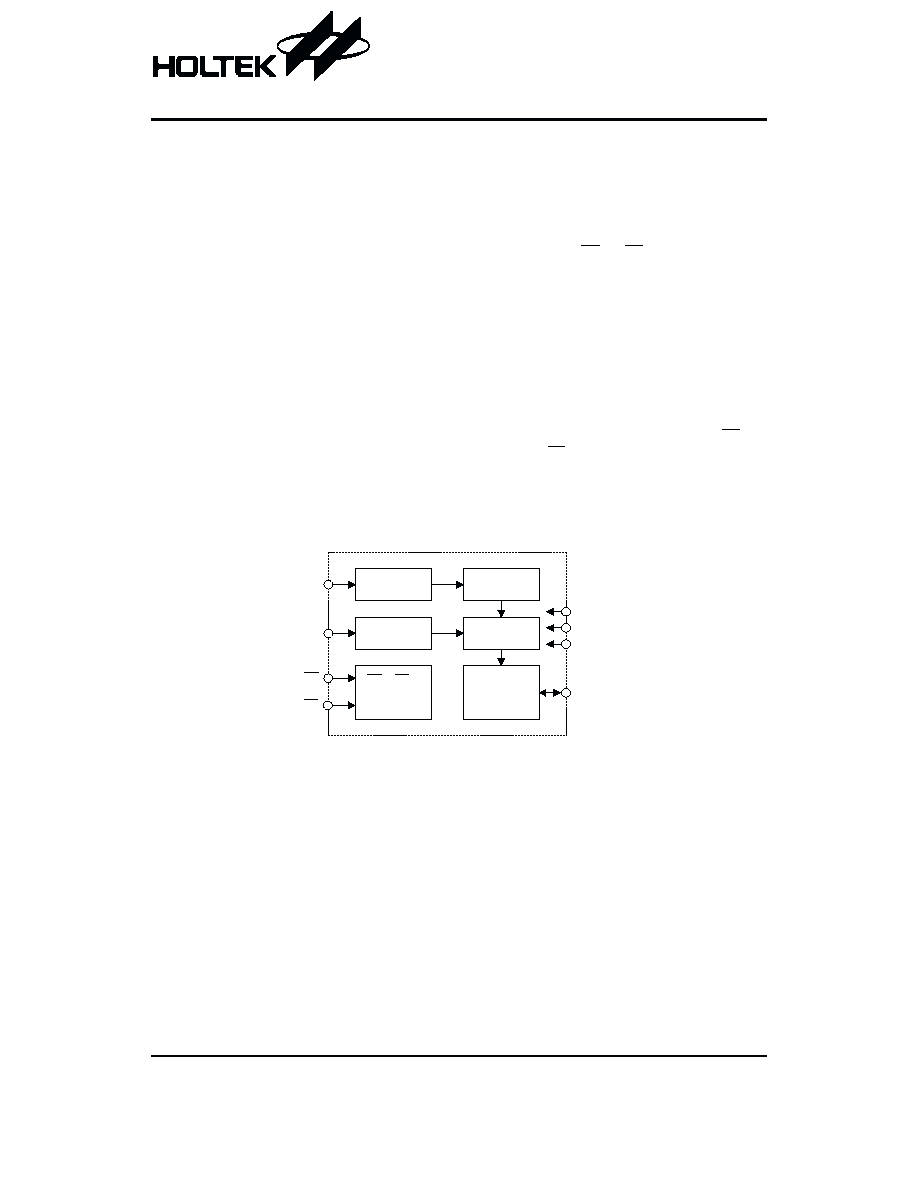
Block Diagram
Rev. 1.10
1
November 21, 2002
Features
·
Operating voltage: +5.0V
·
Programming voltage
-
V
PP
=12.5V
±0.2V
-
V
CC
=6.0V
±0.2V
·
High-reliability CMOS technology
·
Latch-up immunity to 100mA from -1.0V to V
CC
+1.0V
·
CMOS and TTL compatible I/O
·
Low power consumption
-
Active: 30mA max.
-
Standby: 1
mA typ.
·
256K
´16-bits organization
·
Fast read access time: 70ns
·
Fast programming algorithm
·
Programming time 75
ms typ.
·
Two line controls (OE and CE)
·
Standard product identification code
·
Commercial temperature range (0
°C to +70°C)
·
40-pin plastic DIP, 44-pin PLCC package
General Description
The HT27C4096 chip family is a low-power, 4096K
(4,194,304) bits, +5V electrically one-time programma-
ble (OTP) read-only memories (EPROM). Organized
into 256K words with 16 bits per word, it features a fast
single address location programming, typically at 75
ms
per word. Any word can be accessed in less than 70ns
with respect to spec. This eliminates the need for WAIT
states in high-performance microprocessor systems.
The HT27C4096 has separate Output Enable (OE) and
Chip Enable (CE) controls which eliminate bus conten-
tion issues.
X - D e c o d e r
Y - D e c o d e r
C e l l A r r a y
S A C K T
&
O u t p u t B u f f e r
C o l u m n
A d d r e s s
R o w
A d d r e s s
Y - G a t i n g
V C C
D Q 0 ~ D Q 1 5
V S S
C E
O E
V P P
C E & O E &
T E S T
C o n t r o l L o g i c
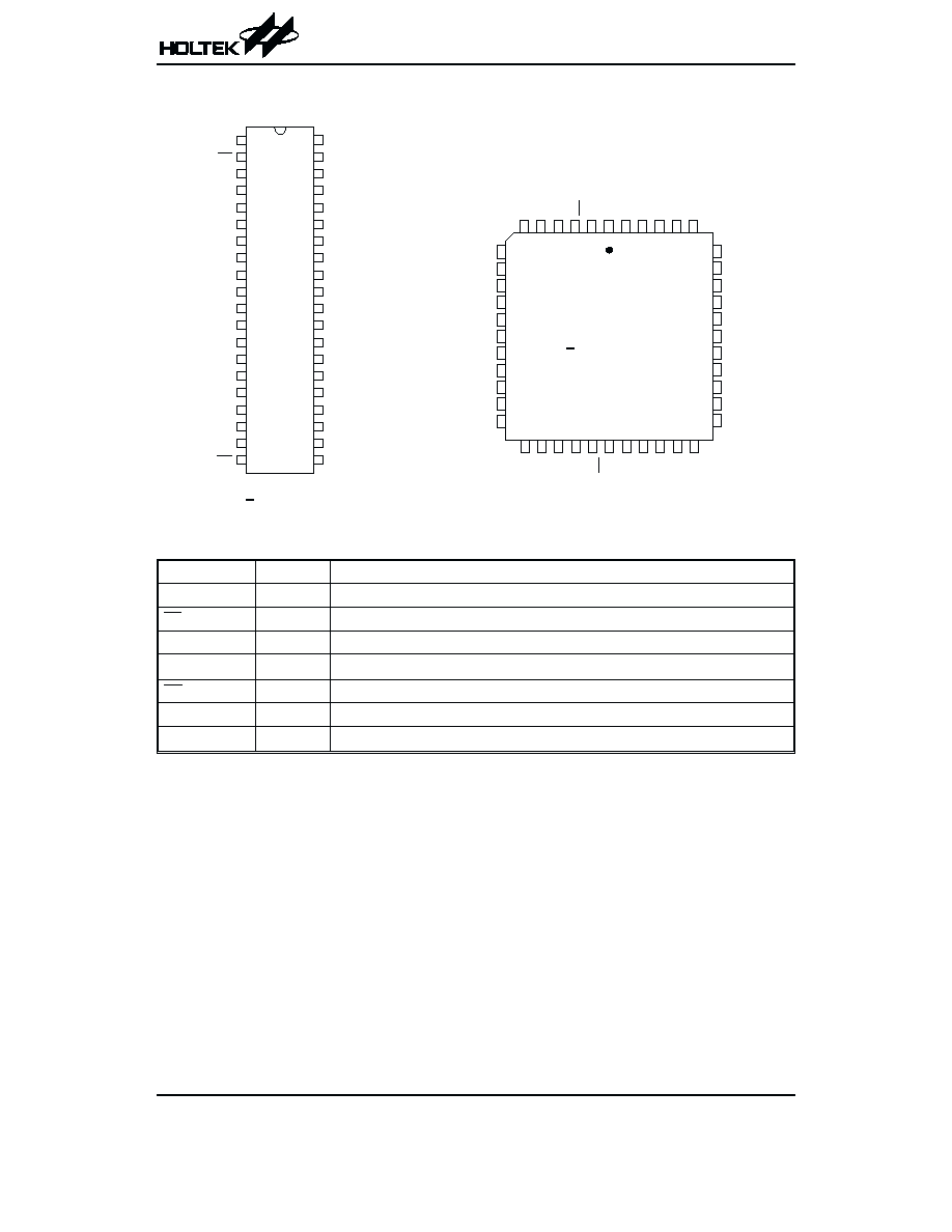
Pin Assignment
Pin Description
Pin Name
I/O/P
Description
VPP
P
Program voltage supply
CE
I
Chip enable
DQ0~DQ15
I/O
Data inputs/outputs
VSS
¾
Negative power supply, ground
OE
I
Output enable
A0~A17
I
Address inputs
VCC
¾
Positive power supply
Absolute Maximum Rating
Operation Temperature Commercial ..........................................................................................................0
°C to +70°C
Storage Temperature.............................................................................................................................
-65°C to 125 °C
Applied V
CC
Voltage with Respect to VSS .................................................................................................
-0.6V to 7.0V
Applied Voltage on Input Pin with Respect to VSS.....................................................................................
-0.6V to 7.0V
Applied Voltage on Output Pin with Respect to VSS .........................................................................
-0.6V to V
CC
+0.5V
Applied Voltage on A9 Pin with Respect to VSS ......................................................................................
-0.6V to 13.5V
Applied V
PP
Voltage with Respect to VSS ................................................................................................
-0.6V to 13.5V
Applied READ Voltage (Functionality is guaranteed between these limits) ..............................................+4.5V to +5.5V
Note: These are stress ratings only. Stresses exceeding the range specified under
²Absolute Maximum Ratings² may
cause substantial damage to the device. Functional operation of this device at other conditions beyond those
listed in the specification is not implied and prolonged exposure to extreme conditions may affect device reliabil-
ity.
HT27C4096
Rev. 1.10
2
November 21, 2002
4 0
3 9
3 8
3 7
3 6
3 5
3 4
3 3
3 2
3 1
3 0
2 9
2 8
2 7
2 6
2 5
2 4
2 3
2 2
2 1
1
2
3
4
5
6
7
8
9
1 0
1 1
1 2
1 3
1 4
1 5
1 6
1 7
1 8
1 9
2 0
H T 2 7 C 4 0 9 6
4 0 D I P - A
2 0 2 1 2 2
1 8 1 9
7
8
9
1 0
1 1
1 2
1 3
1 4
1 5
1 6
1 7
4 4 4 3 4 2 4 1 4 0
D Q 1 2
D Q 1 1
D Q 1 0
D Q 9
D Q 8
V S S
N C
D Q 7
D Q 6
D Q 5
D Q 4
H T 2 7 C 4 0 9 6
4 4 P L C C - A
2 8
2 7
2 6
2 5
2 4
2 3
1
2
3
4
5
6
A
1
4
A
1
5
A
1
6
A
1
7
V
C
C
N
C
V
P
P
C
E
D
Q
1
5
D
Q
1
4
D
Q
1
3
A 1 3
A 1 2
A 1 1
A 1 0
A 9
V S S
N C
A 8
A 7
A 6
A 5
3 9
3 8
3 7
3 6
3 5
3 4
3 3
3 2
3 1
3 0
2 9
V P P
D Q 1 5
D Q 1 4
D Q 1 3
D Q 1 2
D Q 1 1
D Q 1 0
D Q 9
D Q 8
V S S
D Q 7
D Q 6
D Q 5
D Q 4
D Q 3
D Q 2
D Q 1
D Q 0
V C C
A 1 7
A 1 6
A 1 5
A 1 4
A 1 3
A 1 2
A 1 1
A 1 0
A 9
V S S
A 8
A 7
A 6
A 5
A 4
A 3
A 2
A 1
A 0
A
4
A
3
A
2
A
1
A
0
N
C
D
Q
0
D
Q
1
D
Q
2
D
Q
3
C E
O E
O
E

HT27C4096
Rev. 1.10
5
November 21, 2002
Functional Description
Programming of the HT27C4096
When the HT27C4096 is delivered, the chip has all
4096K bits in the
²ONE², or HIGH state. ²ZEROs² are
loaded into the HT27C4096 through programming.
The programming mode is entered when 12.5
±0.2V is ap-
plied to the VPP pin, OE is at V
IH
, and CE is V
IL
. For pro-
gramming, the data to be programmed is applied with 16
bits in parallel to the data pins.
The programming flowchart in Figure 3 shows the fast
interactive programming algorithm. The interactive al-
gorithm reduces programming time by using 50
ms to
105
ms programming pulses and giving each address
only as many pulses as is necessary in order to reliably
program the data. After each pulse is applied to a given
address, the data in that address is verified. If the data
is not verified, additional pulses are given until it is veri-
fied or until the maximum number of pulses is reached
while sequencing through each address of the
HT27C4096. This process is repeated while sequenc-
ing through each address of the HT27C4096. This part
of the programming algorithm is done at V
CC
=6.0V to
assure that each EPROM bit is programmed to a suffi-
ciently high threshold voltage. This ensures that all bits
have sufficient margin. After the final address is com-
pleted, the entire EPROM memory is read at
V
CC
=V
PP
=5.25
±0.25V to verify the entire memory.
Program inhibit mode
Programming of multiple HT27C4096 in parallel with dif-
ferent data is also easily accomplished by using the Pro-
gram Inhibit Mode. Except for CE, all like inputs of the
parallel HT27C4096 may be common. A TTL low-level pro-
gram pulse applied to an HT27C4096 CE input with
Vpp=12.5
±0.2V, and OE HIGH will program that
HT27C4096. A high-level CE input inhibits the HT27C4096
from being programmed.
Program verify mode
Verification should be performed on the programmed
bits to determine whether they were correctly pro-
grammed. The verification should be performed with OE
at V
IL
, and CE at V
IH
, and VPP at its programming volt-
age.
Auto product identification
The Auto Product Identification mode allows the reading
out of a binary code from an EPROM that will identify its
manufacturer and the type. This mode is intended for
programming to automatically match the device to be
programmed with its corresponding programming algo-
rithm. This mode is functional in the 25
°C±5°C ambient
temperature range that is required when programming
the HT27C4096.
To activate this mode, the programming equipment must
force 12.0
±0.5V on the address line A9 of the
HT27C4096. Two identifier bytes may then be sequenced
from the device outputs by toggling address line A0 from
V
IL
to V
IH
, when A1=V
IH
. All other address lines must be
held at V
IH
during Auto Product Identification mode.
Byte 0 (A0=V
IL
) represents the manufacturer code, and
byte 1 (A0=V
IH
), the device code. For HT27C4096, these
two identifier bytes are given in the Operation mode truth
table. When A1=V
IL
, the HT27C4096 will read out the bi-
nary code of 7F, continuation code, to signify the unavail-
ability of manufacturer ID codes.
Read mode
The HT27C4096 has two control functions, both of
which must be logically satisfied in order to obtain data
at outputs. Chip Enable (CE) is the power control and
should be used for device selection. Output Enable (OE)
is the output control and should be used to gate data to
the output pins, independent of device selection. As-
suming that addresses are stable, address access time
(t
ACC
) is equal to the delay from CE to output (t
CE
). Data
is available at the outputs (t
OE
) after the falling edge of
OE, assuming the CE has been LOW and addresses
have been stable for at least t
ACC
-t
OE
.
Standby mode
The HT27C4096 has CMOS standby mode which re-
duces the maximum V
CC
current to 10
mA. It is placed in
CMOS standby when CE is at V
CC
±0.3V. The
HT27C4096 also has a TTL-standby mode which re-
duces the maximum V
CC
current to 1.0mA. It is placed in
TTL-standby when CE is at V
IH
. When in standby mode,
the outputs are in a high-impedance state, independent
of the OE input.
Two-line output control function
To accommodate multiple memory connections, a
two-line control function is provided to allow for:
·
Low memory power dissipation
·
Assurance that output bus contention will not occur
It is recommended that CE be decoded and used as the
primary device-selection function, while OE be made a
common connection to the READ line from the system
control bus. This assures that all deselected memory
devices are in their low-power standby mode and that
the output pins are only active when data is desired from
a particular memory device.
System considerations
During the switch between active and standby condi-
tions, transient current peaks are produced on the rising
and falling edges of Chip Enable. The magnitude of