 | –≠–ª–µ–∫—Ç—Ä–æ–Ω–Ω—ã–π –∫–æ–º–ø–æ–Ω–µ–Ω—Ç: HT2830 | –°–∫–∞—á–∞—Ç—å:  PDF PDF  ZIP ZIP |

HT2830
Up/Down Tone Generator
Pin Assignment
Features
∑
Single power supply: 2.4V~3.3V
∑
Low standby current: 1
µ
A (Typ.)
at V
DD
=3V
∑
Speaker or direct piezo application
∑
Sound output: one Main Tone plus two
Fighting Sounds (1,2)
∑
Two direct LED drive outputs
(The flash rate depends on the sound speed)
∑
Option mode selection: normal mode or auto
mode (bonding option)
∑
Minimum external components
General Description
The HT2830 is a CMOS LSI chip designed for
use in sound effect products. It is a body struc-
ture including tone circuit, noise circuit, an up-
down counter, and other control logic to
generate various sounds such as JET plane,
motorcycle, helicopter, train, and so forth. Fea-
tures from the customer's sound samples can be
analyzed and programmed into an internal
ROM by changing a mask layer during device
fabrication. The HT2830 is suitable for various
toy applications.
1
9th July '97

Block Diagram
Pad Assignment
Chip size: 97
◊
107 (mil)
2
* The IC substrate should be connected to VDD in the PCB layout artwork.
HT2830
2
9th July '97

Pad Coordinates
Unit: mil
Pad No.
X
Y
Pad No.
X
Y
1
≠36.13
24.57
12
36.01
≠40.46
2
≠36.13
16.62
13
36.01
≠33.96
3
≠36.13
≠26.09
14
36.01
≠20.66
4
≠36.13
≠33.96
15
36.01
≠0.88
5
≠36.13
≠40.46
16
36.01
24.24
6
≠29.70
≠40.46
17
36.01
40.46
7
≠23.24
≠40.46
18
≠0.58
40.46
8
≠13.35
≠40.46
19
≠20.13
40.46
9
13.46
≠40.46
20
≠28.24
40.46
10
20.66
≠40.46
21
≠36.25
40.46
11
27.18
≠40.46
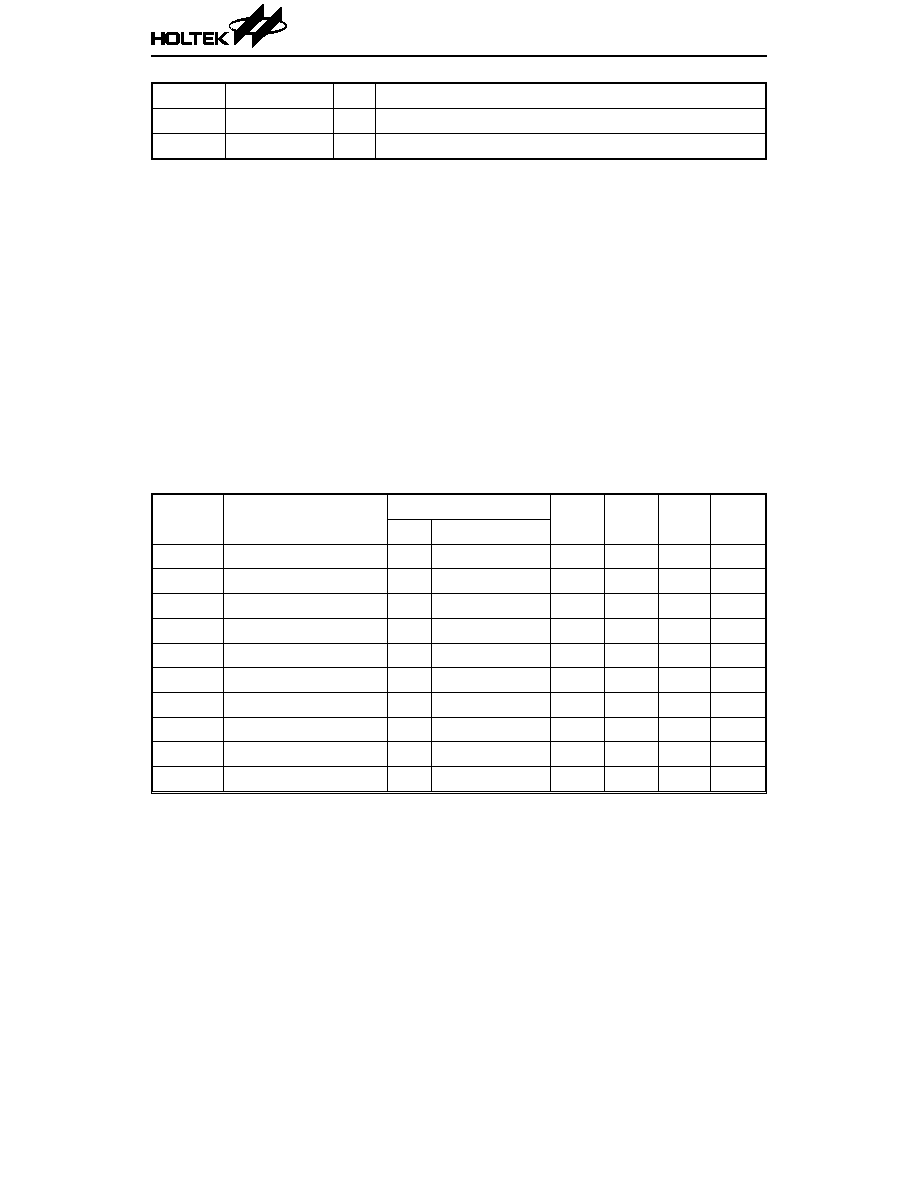
Pad Description
Pad No.
Pad Name
I/O
Description
1
SWAB
I
Fighting sound 1/2 toggle input, low active
2
SWB
I
Fighting sound 2 input, low active
3
SWUP
I
Main tone up input, low active
4
SWDN
I
Main tone down input, low active
5
VSS
--
Negative power supply, GND
6
OPT1
I
Main tone option
7
TEST6
I
For IC test only
8
SWA
I
Fighting sound 1 input, low active
9
TEST5
I
For IC test only
10
OPT2
I
Normal mode/auto mode option
11
VDD
--
Positive power supply
12
TEST3
O
For IC test only
13
LED1
O
LED flash output
14
LED2
O
LED flash output
15
OUT
O
Sound output
16
OUT
O
Sound output, out of phase to pad 15
17
TEST1
O
For IC test only
18
OSC2
O
Oscillator output
19
OSC1
I
Oscillator input
HT2830
3
9th July '97
Pad No.
Pad Name
I/O
Description
20
TEST2
O
For IC test only
21
TEST4
I
For IC test only
(1) OPT1:
Bond pad 5
Main Tone 1
Bond pad 6
Main Tone 2
(2) OPT2:
Bond pad 10
Auto Mode
Bond Pad 11
Normal Mode
Absolute Maximum Ratings*
Supply Voltage ................................. ≠0.3V to 5V
Storage Temperature................. ≠50
∞
C to 125
∞
C
Input Voltage..................V
SS
≠0.3V to V
DD
+0.3V
Operating Temperature................... 0
∞
C to 70
∞
C
*Note: Stresses above those listed under "Absolute Maximum Ratings" may cause permanent
damageto the device. These are stress ratings only. Functional operation of this device at
these or any other conditions above those indicated in the operational sections of this
specification is not implied and exposure to absolute maximum rating conditions for extended
periods may affect device reliability.
Electrical Characteristics
(Ta=25
∞
C)
Symbol
Parameter
Test Conditions
Min.
Typ.
Max.
Unit
V
DD
Conditions
V
DD
Operating Voltage
--
--
2.4
3
3.3
V
I
STB
Standby Current
3V
--
--
1
5
µ
A
I
DD
Operating Current
3V
No load
--
--
150
µ
A
I
OH
OUT Source Current
3V
V
OH
=2.5V
≠2
--
--
mA
I
OL1
OUT Sink Current
3V
V
OL
=0.5V
0.7
--
--
mA
I
OL2
LED1 Sink Current
3V
V
OL
=1V
≠8
--
--
mA
I
OL3
LED2 Sink Current
3V
V
OL
=1V
≠8
--
--
mA
V
IH
"H" Input Voltage
3V
--
2.4
--
--
V
V
OL
"L" Input Voltage
3V
--
--
--
0.6
V
F
OSC
Oscillator Frequency
--
R
OSC
=62k
--
256
--
kHz
HT2830
4
9th July '97

Timing Diagram & Application Circuit
∑
Normal mode (1)
HT2830
5
9th July '97