HT2860
6-Sound Generator
Pin Assignment
General Description
The HT2860 is a CMOS LSI chip designed for
use in sound effect products. It can generate six
sections of programmable sounds. The LSI is
equipped with tone circuit and control logic to
generate various sounds including door bell,
alarm, melodies, etc. Users can play not only
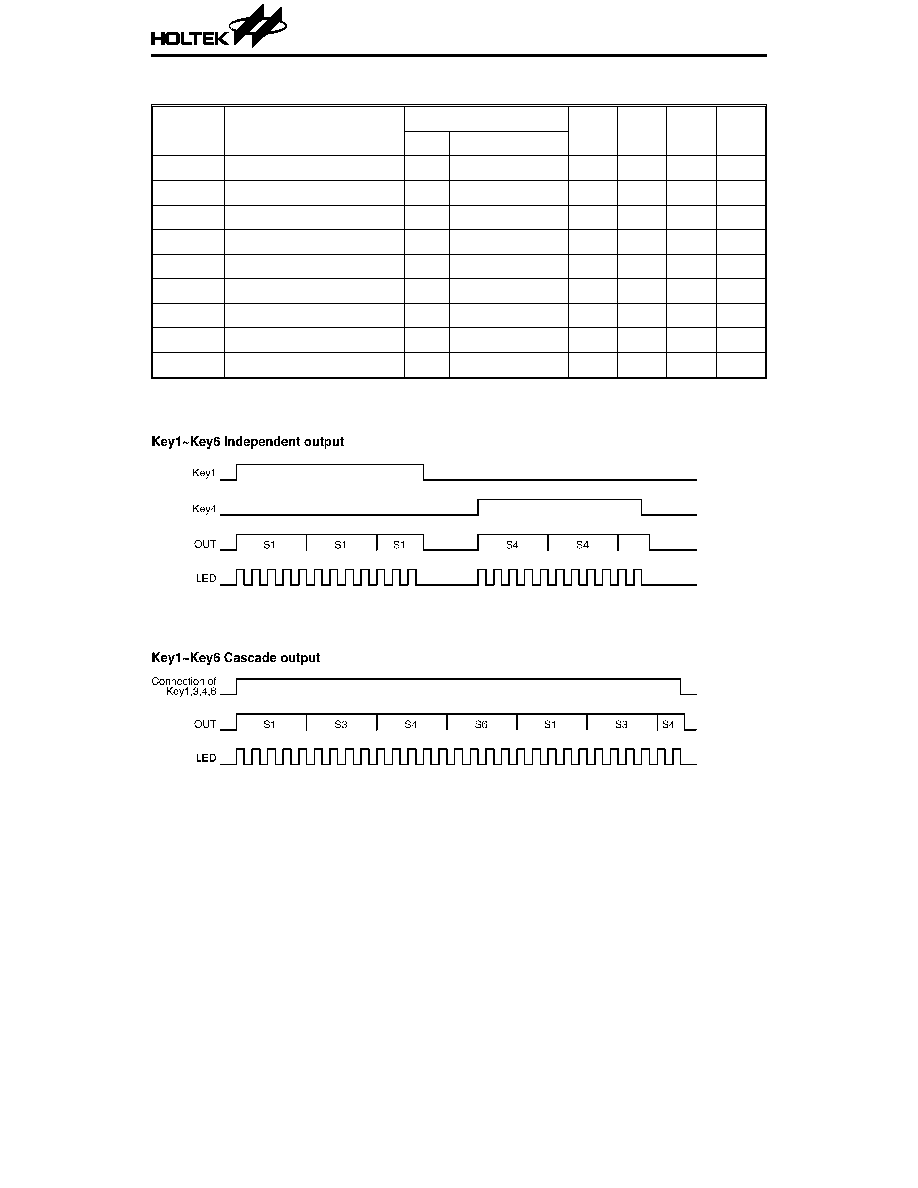
sound sections (S1~S6) by triggering a single
key (K1~K6), but serial sound sections by si-
multaneously triggering more than one key ac-
cording to the key priority where K1 is the
highest and K6 is the lowest. The customer's
sound sample is analyzed and programmed into
an internal ROM by changing a mask layer
during device fabrication. The HT2860 is suit-
able for various toy applications.
Features
·
Single power supply: 2.4V~4.5V
·
Low standby current: 1
µ
A (Typ.)
at V
DD
=3V
·
Auto power-off function
·
Six different sound sections
·
K1 to K6 independently chosen or as
a cascade control
·
Speaker or direct piezo application
·
0.5Hz~1Hz LED flash output
·
Minimal external components
HT2860
18 DIP
18
17
16
15
14
13
12
11
10
1
2
3
4
5
6
7
8
9
OUT
OUT
TEST1
TEST2
PWR
VSS
KEY1
KEY2
KEY3
VDD
KEY6
KEY5
KEY4
KEY3
KEY2
KEY1
VSS
HT2860
16 DIP
OSC3
TEST3
OSC1
OSC2
OUT
OUT
TEST2
PWR
16
15
14
13
12
11
10
9
1
2
3
4
5
6
7
8
OSC2
OSC1
TEST3
LED
OSC3
VDD
KEY6
KEY5
KEY4
1
11th July '97
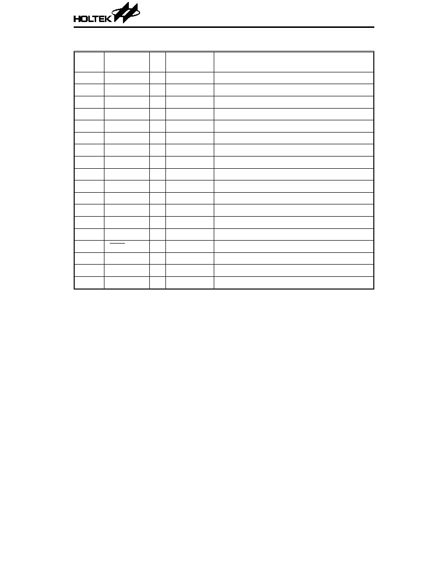
Pad Description
Pad No.
Pad Name
I/O
Internal
Connection
Description
1
LED
O
Inverter Out
LED flash output
2
OSC3
O
--
Vibration oscillator output
3
VDD
--
--
Positive power supply
4
KEY6
I
Pull-Low
KEY6 input, high active
5
KEY5
I
Pull-Low
KEY5 input, high active
6
KEY4
I
Pull-Low
KEY4 input, high active
7
KEY3
I
Pull-Low
KEY3 input, high active
8
KEY2
I
Pull-Low
KEY2 input, high active
9
KEY1
I
Pull-Low
KEY1 input, high active
10
VSS
--
--
Negative power supply, GND
11
PWR
I
--
Power on reset
12
TEST2
I/O
--
For IC test only
13
TEST1
I/O
--
For IC test only
14
OUT
O
Inverter Out
Sound output, normally low at the standby state
15
OUT
O
Inverter Out
Sound output, out of phase to pad 14
16
OSC2
O
--
Oscillator output
17
OSC1
I
--
Oscillator input
18
TEST3
I/O
--
For IC test only
Absolute Maximum Ratings*
Supply Voltage ................................. 0.3V to 5V
Storage Temperature................. 50
°
C to 125
°
C
Input Voltage.................... V
SS
0.3 to V
DD
+0.3V
Operating Temperature................... 0
°
C to 70
°
C
*Note: Stresses above those listed under "Absolute Maximum Ratings" may cause permanent
damageto the device. These are stress ratings only. Functional operation of this device at
these or any other conditions above those indicated in the operational sections of this
specification is not implied and exposure to absolute maximum rating conditions for extended
periods may affect device reliability.
HT2860
3
11th July '97