HT36FA
Music Synthesizer 8-Bit MCU
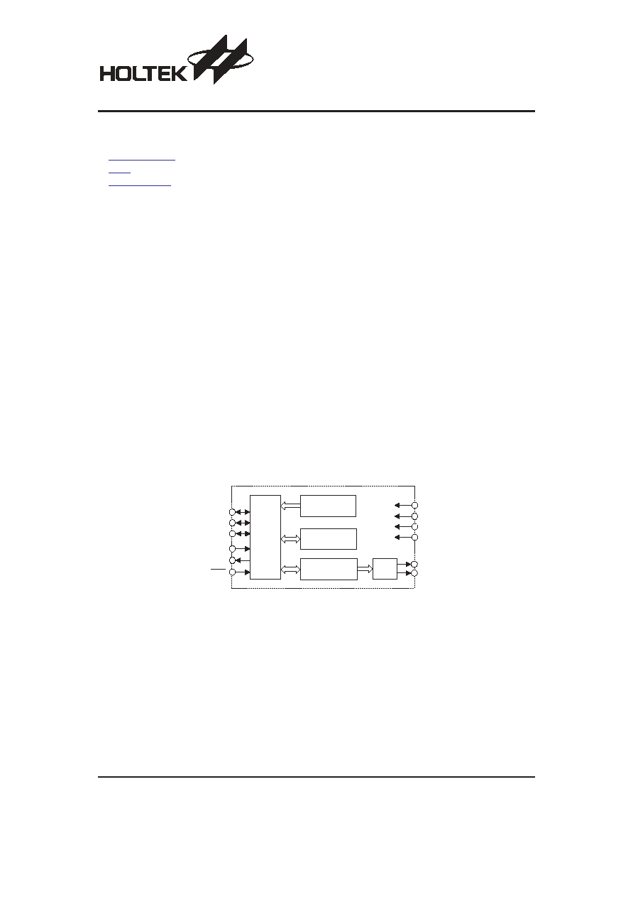
Block Diagram
Rev. 1.10
1
March 13, 2006
Features
·
Operating voltage: 2.4V~5.0V
·
Operating frequency:
X
¢tal: 6MHz~8MHz
R
OSC
: typ. 6MHz
·
Built-in 128K
´16-bit (2M-bit) ROM for program/data
shared
·
Built-in 8 bit MCU with 208
´8 bits RAM
·
Two 8 bit programmable timer with 8 stage prescaler
·
24 bidirectional I/O lines
·
Watchdog timer
·
Four polyphonic synthesizer
·
Stereo 16-bit DAC
·
Oscillation modes: XTAL/RCOSC
·
Low voltage reset
·
Eight-level subroutine nesting
·
Supports 8-bit table read instruction (TBLP)
·
HALT function and wake-up feature reduce power
consumption
·
Bit manipulation instructions
·
63 powerful instructions
·
All instructions in 1 or 2 machine cycles
·
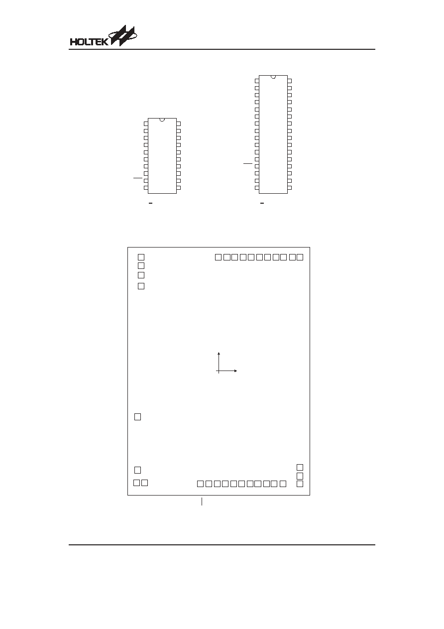
20/32-pin SOP package
General Description
The HT36FA is an 8-bit high performance RISC archi-
tecture microcontroller specifically designed for various
music applications. It provides an 8-bit MCU and a
4-channel Wavetable synthesizer. It has a built-in 8-bit
microprocessor which controls the synthesizer to gen-
erate the melody by setting the special register. A HALT
feature is provided to reduce power consumption.
8 - B i t
M C U
1 2 8 K ´ 1 6 - b i t
R O M
2 0 8 ´ 8
R A M
M u l t i p l i e r / P h a s e
G e n e r a l
P A 0 ~ P A 7
P B 0 ~ P B 7
P C 0 ~ P C 7
O S C 1
O S C 2
R E S
1 6 - B i t
D A C
V D D
V S S
V D D A
L C H
V S S A
R C H
Technical Document
·
Tools Information
·
FAQs
·
Application Note
Pad Coordinates
Unit:
mm
Pad No.
X
Y
Pad No.
X
Y
1
-1003.950
1463.950
18
708.150
-1448.750
2
-1003.950
1350.950
19
818.750
-1448.750
3
-1003.950
1238.510
20
1042.350
-1448.200
4
-1003.950
1089.850
21
1042.350
-1348.200
5
-1042.350
-587.774
22
1042.350
-1237.600
6
-1042.350
-1265.626
23
1041.900
1462.150
7
-1052.100
-1439.900
24
941.900
1462.150
8
-952.100
-1439.900
25
831.300
1462.150
9
-236.026
-1448.750
26
731.300
1462.150
10
-134.250
-1448.750
27
620.700
1462.150
11
-23.650
-1448.750
28
520.700
1462.150
12
76.350
-1448.750
29
410.100
1462.150
13
186.950
-1448.750
30
310.100
1462.150
14
286.950
-1448.750
31
199.500
1462.150
15
397.550
-1448.750
32
99.500
1462.150
16
497.550
-1448.750
33
-11.100
1462.150
17
608.150
-1448.750
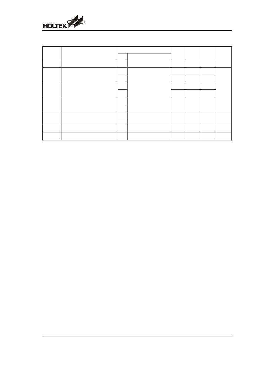
Pad Description
Pad No.
Pad Name
I/O
Internal
Connection
Function
8, 7
VDD, VSS
¾
¾
Digital power supply, ground
3,4
VDDA, VSSA
¾
¾
DAC power supply
18~25
PA0~PA7
I/O
Wake-up,
Pull-high or
None
Bidirectional 8-bit I/O port, wake-up by mask option
33~26
PB0~PB7
I/O
Pull-high or
None
Bidirectional 8-bit I/O port
17~10
PC0~PC7
I/O
Pull-high or
None
Bidirectional 8-bit I/O port
9
RESET
I
¾
Reset input, active low
6
OSC1
I
X
¢tal/Resistor XIN for X¢tal or ROSCIN for resistor by mask option
5
OSC2
O
¾
XOUT or T1
1
RCH
O
¾
DAC output R channel
2
LCH
O
¾
DAC output L channel
Absolute Maximum Ratings
Supply Voltage ..........................V
SS
-0.3V to V
SS
+5.5V
Storage Temperature ...........................
-50°C to 125°C
Input Voltage .............................V
SS
-0
.
3V to V
DD
+0.3V
Operating Temperature ..........................
-25°C to 70°C
Note: These are stress ratings only. Stresses exceeding the range specified under
²Absolute Maximum Ratings² may
cause substantial damage to the device. Functional operation of this device at other conditions beyond those
listed in the specification is not implied and prolonged exposure to extreme conditions may affect device reliabil-
ity.
HT36FA
Rev. 1.10
3
March 13, 2006
HT36FA
Rev. 1.10
5
March 13, 2006
Function Description
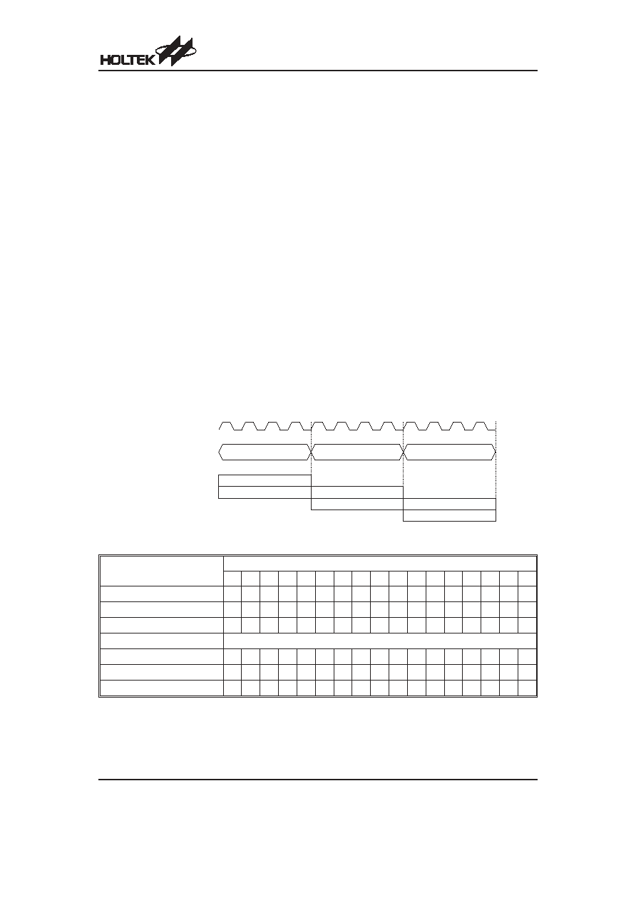
Execution Flow
The system clock for the HT36FA is derived from either
a crystal or an RC oscillator. The oscillator frequency di-
vided by 2 is the system clock for the MCU and it is inter-
nally divided into four non-overlapping clocks. One
instruction cycle consists of four system clock cycles.
Instruction fetching and execution are pipelined in such
a way that a fetch takes one instruction cycle while de-
coding and execution takes the next instruction cycle.
However, the pipelining scheme causes each instruc-
tion to effectively execute in one cycle. If an instruction
changes the program counter, two cycles are required
to complete the instruction.
Program Counter
- PC
The 13-bit program counter (PC) controls the sequence
in which the instructions stored in program ROM are ex-
ecuted and its contents specify a maximum of 8192 ad-
dresses for each bank.
After accessing a program memory word to fetch an in-
struction code, the contents of the program counter are
incremented by one. The program counter then points
to the memory word containing the next instruction
code.
When executing a jump instruction, conditional skip ex-
ecution, loading PCL register, subroutine call, initial re-
set, internal interrupt, external interrupt or return from
subroutine, the PC manipulates the program transfer by
loading the address corresponding to each instruction.
The conditional skip is activated by instruction. Once the
condition is met, the next instruction, fetched during the
current instruction execution, is discarded and a dummy
cycle replaces it to retrieve the proper instruction. Other-
wise proceed with the next instruction.
The lower byte of the program counter (PCL) is a read-
able and writeable register (06H). Moving data into the
PCL performs a short jump. The destination will be
within 256 locations.
Once a control transfer takes place, an additional
dummy cycle is required.
Program ROM
HT36FA provides 18 address lines WA17~WA0 to read
the Program ROM which is up to 2M bits, and is com-
monly used for the wavetable voice codes and the pro-
gram memory. It provides two address types, one type is
for program ROM, which is addressed by a bank pointer
PF3~PF0 and a 13-bit program counter PC12~PC0;
T 1
T 2
T 3
T 4
T 1
T 2
T 3
T 4
T 1
T 2
T 3
T 4
F e t c h I N S T ( P C )
E x e c u t e I N S T ( P C - 1 )
F e t c h I N S T ( P C + 1 )
E x e c u t e I N S T ( P C )
F e t c h I N S T ( P C + 2 )
E x e c u t e I N S T ( P C + 1 )
P C
P C + 1
P C + 2
S y s t e m C l o c k o f M C U
( S y s t e m C l o c k / 2 )
P C
Execution Flow
Mode
Program Counter
*16 *15 *14 *13 *12 *11 *10
*9
*8
*7
*6
*5
*4
*3
*2
*1
*0
Initial Reset
0
0
0
0
0
0
0
0
0
0
0
0
0
0
0
0
0
Timer/Event Counter 0 Overflow PF3 PF2 PF1 PF0
0
0
0
0
0
0
0
0
0
1
0
0
0
Timer/Event Counter 1 Overflow PF3 PF2 PF1 PF0
0
0
0
0
0
0
0
0
0
1
1
0
0
Skip
Program Counter+2
Loading PCL
PF3 PF2 PF1 PF0 *12 *11 *10
*9
*8 @7 @6 @5 @4 @3 @2 @1 @0
Jump, Call Branch
PF3 PF2 PF1 PF0 #12 #11 #10 #9
#8
#7
#6
#5
#4
#3
#2
#1
#0
Return From Subroutine
PF3 PF2 PF1 PF0 S12 S11 S10 S9
S8
S7
S6
S5
S4
S3
S2
S1
S0
Program Counter
Note:
*12~*0: Bits of Program Counter
@7~@0: Bits of PCL
#12~#0: Bits of Instruction Code
S12~S0: Bits of Stack Register
@7~@0: Bits of PCL
PF3~PF0: Bits of Bank Register