 | –≠–ª–µ–∫—Ç—Ä–æ–Ω–Ω—ã–π –∫–æ–º–ø–æ–Ω–µ–Ω—Ç: HT46R221 | –°–∫–∞—á–∞—Ç—å:  PDF PDF  ZIP ZIP |
Document Outline
- ˛ˇ
- ˛ˇ
- ˛ˇ
- ˛ˇ
- ˛ˇ
- ˛ˇ
- ˛ˇ
- ˛ˇ
- ˛ˇ
- ˛ˇ
- ˛ˇ
- ˛ˇ
- ˛ˇ
- ˛ˇ
- ˛ˇ

HT46R22/HT46C22
8-Bit A/D Type MCU
I
2
C is a trademark of Philips Semiconductors
Rev. 1.10
1
October 2, 2002
General Description
The device is an 8-bit high performance RISC-like
microcontroller designed for multiple I/O product appli-
cations. It is particularly suitable for use in products
such as washing machine controllers and home appli-
ances. A HALT feature is included to reduce power con-
sumption.
Features
∑
Operating voltage:
f
SYS
=4MHz: 2.2V~5.5V
f
SYS
=8MHz: 4.5V~5.5V
∑
19 bidirectional I/O lines (max.)
∑
1 interrupt input shared with an I/O line
∑
8-bit programmable timer/event counter with over-
flow interrupt and 7-stage prescaler
∑
On-chip crystal and RC oscillator
∑
Watchdog Timer
∑
2048
¥14 program memory ROM
∑
64
¥8 data memory RAM
∑
Supports PFD for sound generation
∑
HALT function and wake-up feature reduce power
consumption
∑
Up to 0.5
ms instruction cycle with 8MHz system clock
at V
DD
=5V
∑
6-level subroutine nesting
∑
8 channels 9-bit resolution (8-bit accuracy) A/D con-
verter
∑
1-channel (6+2)/(7+1)-bit PWM output shared with
two I/O lines
∑
Bit manipulation instruction
∑
14-bit table read instruction
∑
63 powerful instructions
∑
All instructions in one or two machine cycles
∑
Low voltage reset function
∑
I
2
C BUS (slave mode)
∑
24-pin SKDIP/SOP package

Block Diagram
Pin Assignment
HT46R22/HT46C22
Rev. 1.10
2
October 2, 2002
P A 5 / I N T
O S C 2
O S C 1
R E S
V D D
M U X
P A C
P A
P O R T A
P A 4 / T M R
S Y S C L K / 4
W D T
P D C
P D
P O R T D
P D 0 / P W M
P O R T B
T M R
T M R C
V S S
P r e s c a l e r
f
S Y S
P A 4
P r o g r a m
R O M
P r o g r a m
C o u n t e r
I n t e r r u p t
C i r c u i t
S T A C K
I N T C
D A T A
M e m o r y
I n s t r u c t i o n
R e g i s t e r
M
U
X
I n s t r u c t i o n
D e c o d e r
S T A T U S
A L U
S h i f t e r
T i m i n g
G e n e r a t o r
A C C
R C O S C
W D T
P r e s c a l e r
M
U
X
M
U
X
M P
P B
P B C
P B 0 / A N 0 ~ P B 7 / A N 7
P A 0 ~ P A 2
P A 3 / P . D
P A 4 / T M R
P A 5 / I N T
P A 6 / S D A
P A 7 / S C L
P W M
8 - C h a n n e l
A / D C o n v e r t e r
P A 3 / P . D
L V R
P A 3 , P A 5
P C
P C C
P C 0 ~ P C 1
I C B U S
S l a v e M o d e
2
H T 4 6 R 2 2 / H T 4 6 C 2 2
2 4 S K D I P - A / S O P - A
P B 5 / A N 5
P B 4 / A N 4
P A 3 / P . D
P A 2
P A 1
P A 0
P B 3 / A N 3
P B 2 / A N 2
P B 1 / A N 1
P B 0 / A N 0
V S S
P C 0
P B 6 / A N 6
P B 7 / A N 7
P A 4 / T M R
P A 5 / I N T
P A 6 / S D A
P A 7 / S C L
O S C 2
O S C 1
V D D
R E S
P D 0 / P W M
P C 1
2 4
2 3
2 2
2 1
2 0
1 9
1 8
1 7
1 6
1 5
1 4
1 3
1
2
3
4
5
6
7
8
9
1 0
1 1
1 2
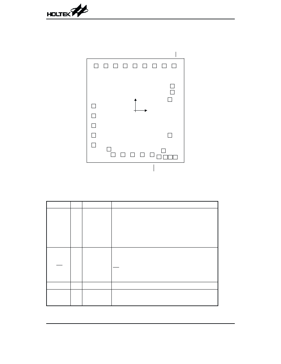
Pad Assignment
HT46C22
* The IC substrate should be connected to VSS in the PCB layout artwork.
Pad Description
Pad Name
I/O
Options
Description
PB0/AN0
PB1/AN1
PB2/AN2
PB3/AN3
PB4/AN4
PB5/AN5
PB6/AN6
PB7/AN7
I/O
Pull-high
Bidirectional 8-bit input/output port. Software instructions deter-
mine the CMOS output, Schmitt trigger input with or without
pull-high resistor (determined by pull-high option: port option) or
A/D input.
Once a PB line is selected as an A/D input (by using software
control), the I/O function and pull-high resistor are disabled auto-
matically.
PA0~PA2
PA3/PFD
PA4/TMR
PA5/INT
PA6/SDA
PA7/SCL
I/O
Pull-high
Wake-up
PA3 or PFD
I/O or Serial Bus
Bidirectional 8-bit input/output port. Each bit can be configured as
wake-up input by options. Software instructions determine the
CMOS output or Schmitt trigger input with or without pull-high resis-
tor (determined by pull-high options: bit option). The PFD, TMR and
INT are pin-shared with PA3, PA4 and PA5, respectively. Once
the I
2
C BUS function is used, the internal registers related to PA6
and PA7 can not be used.
VSS
æ
æ
Negative power supply, ground.
PC0~PC1
I/O
Pull-high
Bidirectional 2-bit input/output port. Software instructions deter-
mine the CMOS output, Schmitt trigger input with or without
pull-high resistor (determine by pull-high option: port option).
HT46R22/HT46C22
Rev. 1.10
3
October 2, 2002
( 0 , 0 )
1
2
3
4
5
6
7
8
9
1 0
1 1
1 2
1 3
1 4
1 5
1 6 1 7
2 1
2 0
1 9
1 8
2 9
2 8
2 7
2 6
2 5
2 4
2 3
2 2
P A 1
P A 0
P B 3 / A N 3
P B 2 / A N 2
P B 1 / A N 1
P B 0 / A N 0
V D D
V S S
T
E
S
T
3
T
E
S
T
2
T
E
S
T
1
R
E
S
P
D
0
/
P
W
M
P
C
1
P
C
0
V
S
S
V
D
D
P A 6 / S D A
P A 7 / S C L
O S C 2
O S C 1
P
A
5
/
I
N
T
P
A
4
/
T
M
R
P
B
7
/
A
N
7
P
B
6
/
A
N
6
P
B
5
/
A
N
5
P
B
4
/
A
N
4
P
A
3
/
P
.
D
P
A
2

Pad Name
I/O
Options
Description
PD0/PWM
I/O
Pull-high
I/O or PWM
Bidirectional 1-bit input/output port. Software instructions deter-
mine the CMOS output, Schmitt trigger input with or without a
pull-high resistor (determined by pull-high option: port option).
The PWM output function is pin-shared with PD0 (dependent on
PWM optios).
RES
I
æ
Schmitt trigger reset input. Active low.
VDD
æ
æ
Positive power supply
OSC1
OSC2
I
O
Crystal or RC
OSC1, OSC2 are connected to an RC network or a Crystal (de-
termined by options) for the internal system clock. In the case of
RC operation, OSC2 is the output terminal for 1/4 system clock.
TEST1
TEST2
TEST3
I
æ
TEST mode input pin
It disconnects in normal operation
Absolute Maximum Ratings
Supply Voltage ...........................V
SS
-0.3V to V
SS
+5.5V
Storage Temperature ............................
-50∞C to 125∞C
Input Voltage..............................V
SS
-0.3V to V
DD
+0.3V
Operating Temperature...........................
-40∞C to 85∞C
Note: These are stress ratings only. Stresses exceeding the range specified under
≤Absolute Maximum Ratings≤ may
cause substantial damage to the device. Functional operation of this device at other conditions beyond those
listed in the specification is not implied and prolonged exposure to extreme conditions may affect device reliabil-
ity.
D.C. Characteristics
Ta=25
∞C
Symbol
Parameter
Test Conditions
Min.
Typ.
Max.
Unit
V
DD
Conditions
V
DD1
Operating Voltage
æ f
SYS
=4MHz
2.2
æ
5.5
V
V
DD2
Operating Voltage
æ f
SYS
=8MHz
4.5
æ
5.5
V
I
DD1
Operating Current (Crystal OSC)
3V
No load, f
SYS
=4MHz
ADC disable
æ
0.6
1.5
mA
5V
æ
2
4
mA
I
DD2
Operating Current (RC OSC)
3V
No load, f
SYS
=4MHz
ADC disable
æ
0.8
1.5
mA
5V
æ
2.5
4
mA
I
DD3
Operating Current
5V
No load, f
SYS
=8MHz
ADC disable
æ
3
5
mA
I
ADC
Only ADC Enable, Others Disable
3V
No load
æ
0.5
1
mA
5V
æ
1.5
3
mA
I
STB1
Standby Current (WDT Enabled)
3V
No load, system HALT
æ
æ
5
mA
5V
æ
æ
10
mA
I
STB2
Standby Current (WDT Disabled)
3V
No load, system HALT
æ
æ
1
mA
5V
æ
æ
2
mA
V
AD
A/D Input Voltage
æ
æ
0
æ
V
DD
V
V
IL1
Input Low Voltage for I/O Ports,
TMR and INT
3V
æ
0
æ
0.3V
DD
V
5V
æ
0
æ
0.3
V
HT46R22/HT46C22
Rev. 1.10
4
October 2, 2002

Symbol
Parameter
Test Conditions
Min.
Typ.
Max.
Unit
V
DD
Conditions
V
IH1
Input High Voltage for I/O Ports,
TMR and INT
3V
æ
0.7V
DD
æ
V
DD
V
5V
æ
0.7V
DD
æ
V
DD
V
V
IL2
Input Low Voltage (RES)
3V
æ
0
æ
0.4V
DD
V
5V
æ
0
æ
0.4V
DD
V
V
IH2
Input High Voltage (RES)
3V
æ
0.9V
DD
æ
V
DD
V
5V
æ
0.9V
DD
æ
V
DD
V
V
LVR
Low Voltage Reset
æ
æ
2.7
3
3.3
V
I
OL
I/O Port Sink Current
3V
V
OL
=0.1V
DD
4
8
æ
mA
5V
V
OL
=0.1V
DD
10
20
æ
mA
I
OH
I/O Port Source Current
3V
V
OH
=0.9V
DD
-2
-4
æ
mA
5V
V
OH
=0.9V
DD
-5
-10
æ
mA
R
PH
Pull-high Resistance
3V
æ
40
60
80
k
W
5V
æ
10
30
50
k
W
E
AD
A/D Conversion Error
æ
æ
æ
±0.5
±1
LSB
A.C. Characteristics
Ta=25
∞C
Symbol
Parameter
Test Conditions
Min.
Typ.
Max.
Unit
V
DD
Conditions
f
SYS1
System Clock (Crystal OSC)
3V
æ
400
æ
4000
kHz
5V
æ
400
æ
8000
kHz
f
SYS2
System Clock (RC OSC)
3V
æ
400
æ
4000
kHz
5V
æ
400
æ
8000
kHz
f
TIMER
Timer I/P Frequency (TMR)
3V
æ
0
æ
4000
kHz
5V
æ
0
æ
8000
kHz
t
AD
A/D Clock Period
5V
æ
1
æ
æ
ms
t
ADC
A/D Conversion Time
æ
æ
æ
76
æ
t
AD
t
WDTOSC
Watchdog Oscillator
3V
æ
43
86
168
ms
5V
æ
35
65
130
ms
t
RES
External Reset Low Pulse Width
æ
æ
1
æ
æ
ms
t
SST
System Start-up Timer Period
æ Wake-up from HALT
æ
1024
æ
*t
SYS
t
INT
Interrupt Pulse Width
æ
æ
1
æ
æ
ms
t
IIC
I
2
C BUS Clock Period
æ
Connect to external
pull-high resistor 2k
W
64
æ
æ
*t
SYS
t
OPT
Option Load Time During Reset
3V
System power on, WDT
time-out at normal mode,
RES is reset
45
90
180
ms
5V
35
70
140
ms
Note: *t
SYS
=1/f
SYS
HT46R22/HT46C22
Rev. 1.10
5
October 2, 2002