 | ÐлекÑÑоннÑй компоненÑ: HT46R46-H | СкаÑаÑÑ:  PDF PDF  ZIP ZIP |
Äîêóìåíòàöèÿ è îïèñàíèÿ www.docs.chipfind.ru

HT46R46-H
Cost-Effective A/D Type 8-Bit OTP MCU
Rev. 1.40
1
March 1, 2006
General Description
The HT46R46-H are 8-bit, high performance, RISC ar-
chitecture microcontroller devices specifically designed
for A/D applications that interface directly to analog sig-
nals, such as those from sensors.
The advantages of low power consumption, I/O flexibil-
ity, programmable frequency divider, timer functions,
oscillator options, multi-channel A/D Converter, Pulse
Width Modulation function, HALT and wake-up func-
tions, enhance the versatility of these devices to suit a
wide range of A/D application possibilities such as sen-
sor signal processing, motor driving, industrial control,
consumer products, subsystem controllers, etc.
The higher operating voltage range and higher operat-
ing temperature range of
-40°C to +125°C for the
HT46R46-H make this series suitable for automotive
applications as well.
Features
·
Operating voltage:
f
SYS
=4MHz: V
LVR
~5.5V with LVR enabled
f
SYS
=8MHz: 3.3V~5.5V with LVR disabled
·
13 bidirectional I/O lines (max.)
·
1 interrupt input shared with an I/O line
·
8-bit programmable timer/event counter with overflow
interrupt and 7-stage prescaler
·
On-chip crystal and RC oscillator
·
Watchdog Timer
·
1024
´14 program memory
·
64
´8 data memory RAM
·
Supports PFD for sound generation
·
HALT function and wake-up feature reduce power
consumption
·
Up to 0.5
ms instruction cycle with 8MHz system clock
at V
DD
=5V
·
4-level subroutine nesting
·
4 channels 8-bit resolution A/D converter
·
1 channel 8-bit PWM output shared with an I/O line
·
Bit manipulation instruction
·
14-bit table read instruction
·
63 powerful instructions
·
All instructions in one or two machine cycles
·
Low voltage reset function
·
18-pin DIP/SOP package
Technical Document
·
Tools Information
·
FAQs
·
Application Note
-
HA0003E Communicating between the HT48 & HT46 Series MCUs and the HT93LC46 EEPROM
-
HA0009E HT48 & HT46 MCU I/O Port Application - Rolling LED Light Display
-
HA0049E Read and Write Control of the HT1380
-
HA0052E Microcontroller Application - Battery Charger
-
HA0083E Li Battery Charger Demo Board - Using the HT46R46
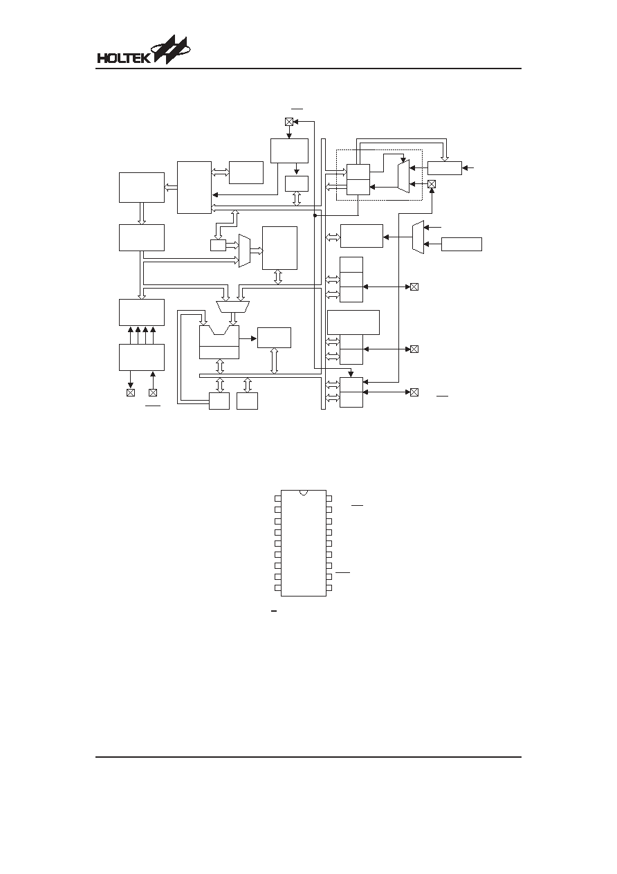
Block Diagram
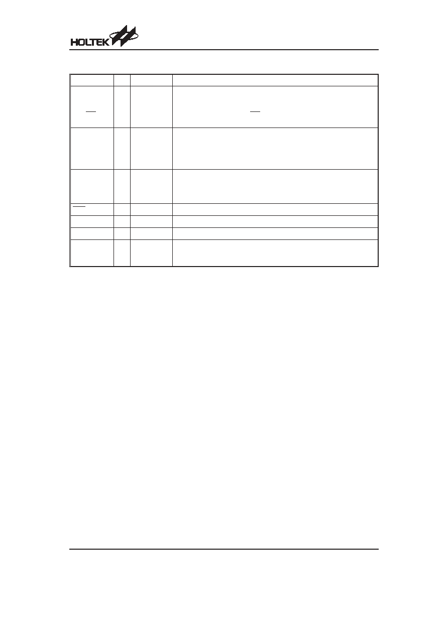
Pin Assignment
HT46R46-H
Rev. 1.40
2
March 1, 2006
P A 5 / I N T
O S C 2
O S C 1
R E S
V D D
M U X
P A C
P A
P o r t A
P o r t D
P o r t B
V S S
P A 4
P r o g r a m
R O M
P r o g r a m
C o u n t e r
I n t e r r u p t
C i r c u i t
S T A C K
I N T C
D A T A
M e m o r y
I n s t r u c t i o n
R e g i s t e r
M
U
X
I n s t r u c t i o n
D e c o d e r
S T A T U S
A L U
S h i f t e r
T i m i n g
G e n e r a t o r
W D T
M
U
X
M P
P A 3 / P F D
P A 3 , P A 5
W D T O S C
f
S Y S
/ 4
T M R
T M R C
P r e s c a l e r
f
S Y S
M
U
X
P A 4 / T M R
P D 0 / P W M
P D
P D C
P W M
4 - C h a n n e l
A / D C o n v e r t e r
P B
P B C
P B 0 / A N 0 ~ P B 3 / A N 3
P A 0 ~ P A 2
P A 3 / P F D
P A 4 / T M R
P A 5 / I N T
P A 6 ~ P A 7
L V R
A C C
P A 4 / T M R
P A 5 / I N T
P A 6
P A 7
O S C 2
O S C 1
V D D
R E S
P D 0 / P W M
P A 3 / P F D
P A 2
P A 1
P A 0
P B 3 / A N 3
P B 2 / A N 2
P B 1 / A N 1
P B 0 / A N 0
V S S
1 8
1 7
1 6
1 5
1 4
1 3
1 2
1 1
1 0
1
2
3
4
5
6
7
8
9
H T 4 6 R 4 6 - H
1 8 D I P - A / S O P - A
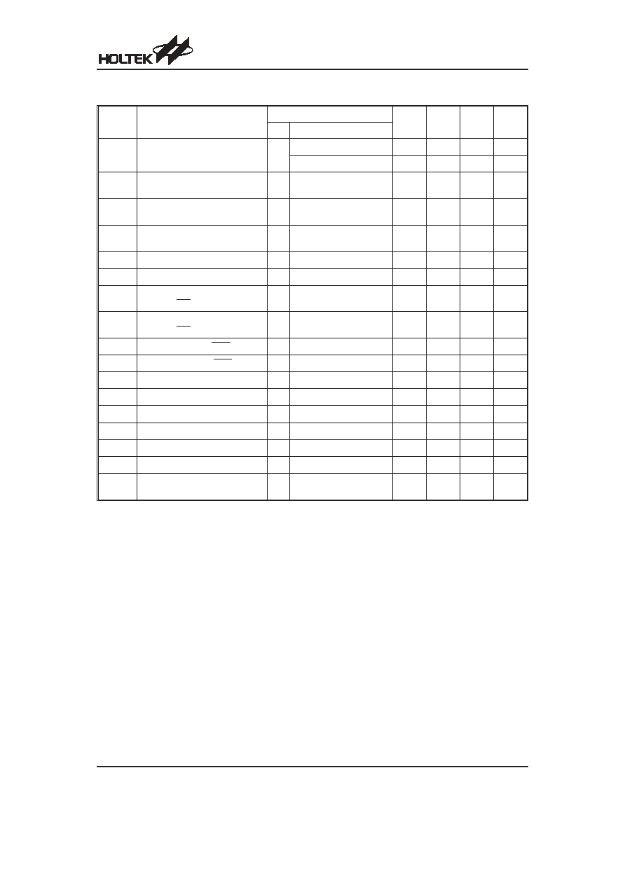
Pin Description
Pin Name
I/O
Options
Description
PA0~PA2
PA3/PFD
PA4/TMR
PA5/INT
PA6, PA7
I/O
Pull-high
Wake-up
PA3 or PFD
Bidirectional 8-bit input/output port. Each bit can be configured as wake-up
input by options. Software instructions determine the CMOS output or Schmitt
trigger input with or without pull-high resistor (determined by pull-high options: bit
option). The PFD, TMR and INT are pin-shared with PA3, PA4 and PA5, re-
spectively.
PB0/AN0
PB1/AN1
PB2/AN2
PB3/AN3
I/O
Pull-high
Bidirectional 4-bit input/output port. Software instructions determine the
CMOS output, Schmitt trigger input with or without pull-high resistor (deter-
mined by pull-high options: bit option) or A/D input.
Once a PB line is selected as an A/D input (by using software control), the I/O
function and pull-high resistor are disabled automatically.
PD0/PWM
I/O
Pull-high
PD0 or PWM
Bidirectional I/O line. Software instructions determine the CMOS output,
Schmitt trigger input with or without a pull-high resistor (determined by
pull-high options: bit option). The PWM output function is pin-shared with
PD0 (dependent on PWM options).
RES
I
¾
Schmitt trigger reset input. Active low.
VDD
¾
¾
Positive power supply
VSS
¾
¾
Negative power supply, ground.
OSC1
OSC2
I
O
Crystal
or RC
OSC1, OSC2 are connected to an RC network or a Crystal (determined by
options) for the internal system clock. In the case of RC operation, OSC2 is
the output terminal for 1/4 system clock.
Absolute Maximum Ratings
Supply Voltage ...........................V
SS
-0.3V to V
SS
+6.0V
Storage Temperature ............................
-50°C to 125°C
Input Voltage..............................V
SS
-0.3V to V
DD
+0.3V
Operating Temperature.........................
-40°C to 125°C
Note: These are stress ratings only. Stresses exceeding the range specified under
²Absolute Maximum Ratings² may
cause substantial damage to the device. Functional operation of this device at other conditions beyond those
listed in the specification is not implied and prolonged exposure to extreme conditions may affect device reliabil-
ity.
HT46R46-H
Rev. 1.40
3
March 1, 2006
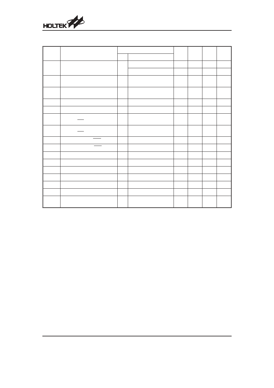
D.C. Characteristics
Ta=25
°C
Symbol
Parameter
Test Conditions
Min.
Typ.
Max.
Unit
V
DD
Conditions
V
DD
Operating Voltage
¾
f
SYS
=4MHz, LVR enabled
V
LVR
¾
5.5
V
f
SYS
=8MHz, LVR disabled
3.3
¾
5.5
V
I
DD1
Operating Current (Crystal OSC)
5V
No load, f
SYS
=4MHz
ADC disabled
¾
2
4
mA
I
DD2
Operating Current (RC OSC)
5V
No load, f
SYS
=4MHz
ADC disabled
¾
2.5
4
mA
I
DD3
Operating Current
(Crystal OSC, RC OSC)
5V
No load, f
SYS
=8MHz
ADC disabled
¾
4
8
mA
I
STB1
Standby Current (WDT Enabled)
5V
No load, system HALT
¾
¾
10
mA
I
STB2
Standby Current (WDT Disabled)
5V
No load, system HALT
¾
¾
2
mA
V
IL1
Input Low Voltage for I/O Ports,
TMR and INT
¾
¾
0
¾
0.3V
DD
V
V
IH1
Input High Voltage for I/O Ports,
TMR and INT
¾
¾
0.7V
DD
¾
V
DD
V
V
IL2
Input Low Voltage (RES)
¾
¾
0
¾
0.4V
DD
V
V
IH2
Input High Voltage (RES)
¾
¾
0.9V
DD
¾
V
DD
V
V
LVR
Low Voltage Reset
¾
¾
3.4
3.8
4.2
V
I
OL
I/O Port Sink Current
5V
V
OL
=0.1V
DD
10
20
¾
mA
I
OH
I/O Port Source Current
5V
V
OH
=0.9V
DD
-5
-10
¾
mA
R
PH
Pull-high Resistance
5V
¾
10
30
50
k
W
V
AD
A/D Input Voltage
¾
¾
0
¾
V
DD
V
E
AD
A/D Conversion Error
¾
¾
¾
±0.5
±1
LSB
I
ADC
Additional Power Consumption
if A/D Converter is Used
5V
¾
¾
1.5
3
mA
HT46R46-H
Rev. 1.40
4
February 24, 2006
Ta=125
°C
Symbol
Parameter
Test Conditions
Min.
Typ.
Max.
Unit
V
DD
Conditions
V
DD
Operating Voltage
¾
f
SYS
=4MHz, LVR enabled
V
LVR
¾
5.5
V
f
SYS
=8MHz, LVR disabled
3.3
¾
5.5
V
I
DD1
Operating Current
(Crystal OSC, RC OSC)
5V
No load, f
SYS
=4MHz
ADC disabled
¾
2.5
4
mA
I
DD2
Operating Current
(Crystal OSC, RC OSC)
5V
No load, f
SYS
=8MHz
ADC disabled
¾
4
8
mA
I
STB1
Standby Current (WDT Enabled)
5V
No load, system HALT
¾
¾
40
mA
I
STB2
Standby Current (WDT Disabled)
5V
No load, system HALT
¾
¾
30
mA
V
IL1
Input Low Voltage for I/O Ports,
TMR and INT
¾
¾
0
¾
0.3V
DD
V
V
IH1
Input High Voltage for I/O Ports,
TMR and INT
¾
¾
0.7V
DD
¾
V
DD
V
V
IL2
Input Low Voltage (RES)
¾
¾
0
¾
0.4V
DD
V
V
IH2
Input High Voltage (RES)
¾
¾
0.9V
DD
¾
V
DD
V
V
LVR
Low Voltage Reset
¾
¾
2.4
2.7
2.9
V
I
OL
I/O Port Sink Current
5V
V
OL
=0.1V
DD
7.5
15
¾
mA
I
OH
I/O Port Source Current
5V
V
OH
=0.9V
DD
-5
-10
¾
mA
R
PH
Pull-high Resistance of I/O Ports
5V
¾
15
40
60
k
W
V
AD
A/D Input Voltage
¾
¾
0
¾
V
DD
V
E
AD
A/D Conversion Error
¾
¾
¾
±1
±2
LSB
I
ADC
Additional Power Consumption
if A/D Converter is Used
5V
¾
¾
1.5
3
mA
HT46R46-H
Rev. 1.40
5
March 1, 2006
Document Outline
- þÿ
- þÿ
- þÿ
- þÿ
- þÿ
- þÿ
- þÿ
- þÿ
- þÿ
- þÿ
- þÿ
- þÿ
- þÿ
- þÿ
- þÿ