 | ÐлекÑÑоннÑй компоненÑ: HT47C20 | СкаÑаÑÑ:  PDF PDF  ZIP ZIP |
Äîêóìåíòàöèÿ è îïèñàíèÿ www.docs.chipfind.ru

HT47C20
8-Bit Microcontroller
1
January 18, 2000
Features
·
Operating voltage: 2.4V~3.6V
·
Eight bidirectional I/O lines
·
Four input lines
·
One interrupt input
·
One 16-bit programmable timer/event
counter with PFD (programmable
frequency divider) function
·
On-chip crystal and RC oscillator for system
clock
·
One 32.768kHz crystal oscillator for real
time clock
·
Watchdog timer
·
2K ´ 16 program memory ROM
·
64 ´ 8 data memory RAM
·
One Real Time Clock (RTC)
·
One 8-bit prescaler for RTC
·
One buzzer output
·
Halt function and wake-up feature reduce
power consumption
·
LCD bias C type
·
OneLCDdriverwith20´3or19´4 segments
·
One 38kHz or 40kHz IR carrier output
(455kHz or 480kHz system clock only)
·
Two channels RC type A/D converter
·
Four-level subroutine nesting
·
Bit manipulation instruction
·
16-bit table read instruction
·
Up to 8.3ms instruction cycle with 480kHz
system clock
·
All instructions in one or two machine cycles
·
63 powerful instructions
General Description
The HT47C20 is an 8-bit high performance
RISC-like microcontroller. Its single cycle in-
struction and two-stage pipeline architecture
make high speed applications. The device is
suited for use in multiple LCD low power
applications among which are calculators, clock
timers, games, scales, toys, thermometers, hy-
grometers, body thermometers, capacitor scaler,
other hand held LCD products, and battery sys-
tems in particular.
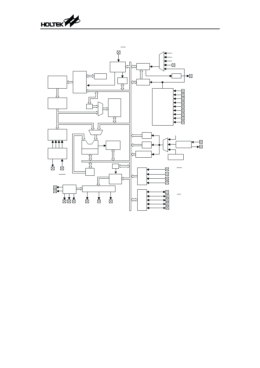
Block Diagram
HT47C20
2
January 18, 2000
M
U
X
P B 0 / I N T
P r o g r a m
C o u n t e r
P r o g r a m
R O M
I n s t r u c t i o n
R e g i s t e r
I n s t r u c t i o n
D e c o d e r
T i m i n g
G e n e r a t o r
O S C 2
O S C 1
R E S
V D D
V S S
I n t e r r u p t
C i r c u i t
I N T C
M P
M
U
X
M U X
D A T A
M e m o r y
A L U
S h i f t e r
S T A T U S
A C C
P A
P o r t A
P A 0 / B Z
T i m e r A
S y s t e m C l o c k
M
U
X
S Y S C L K / 4
P B
P o r t B
P B 2 / T M R
W D T O S C
P A 1 / B Z
P A 2 / I R
P A 3 / P F D
P A 4 ~ P A 7
P B 0 / I N T
P B 1
P B 3
R T C O S C
O S C 3
O S C 4
R T C
S T A C K
L C D
M e m o r y
B P
L C D D r i v e r
C O M 0 ~
C O M 2
C O M 3 /
S E G 1 9
S E G 0 ~
S E G 1 8
T i m e B a s e
W D T
T i m e r B
T 1
R T C O u t p u t
P B 2 / T M R
P F D
P A 3 / P F D
O v e r f l o w
R C T y p e
A / D C o n v e r t e r
A / D C l o c k
I N 0
C S 0
R S 0
C R T 0
R T 0
I N 1
C S 1
R S 1
R T 1
H a l v e
V o l t a g e
V 1 V 2 V 3
C 1
C 2
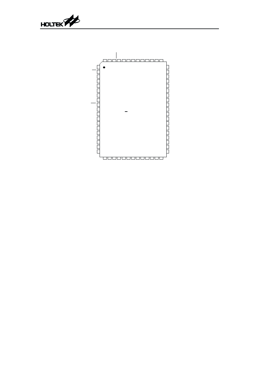
Pin Assignment
HT47C20
3
January 18, 2000
S E G 0
S E G 1
S E G 2
S E G 3
S E G 4
S E G 5
S E G 6
S E G 7
S E G 8
S E G 9
S E G 1 0
S E G 1 1
S E G 1 2
S E G 1 3
S E G 1 4
S E G 1 5
S E G 1 6
S E G 1 7
S E G 1 8
2 0 2 1 2 2 2 3 2 4 2 5 2 6 2 7 2 8 2 9 3 0 3 1 3 2
1
2
3
4
5
6
7
8
9
1 0
1 1
1 2
1 3
1 4
1 5
1 6
1 7
1 8
1 9
5 1
5 0
4 9
4 8
4 7
4 6
4 5
4 4
4 3
4 2
4 1
4 0
3 9
3 8
3 7
3 6
3 5
3 4
3 3
6 1 6 0 5 9 5 8 5 7 5 6 5 5 5 4 5 3 5 2
6 4 6 3 6 2
RT
1
RS
1
CS
1
IN
1
CRT
0
RT
0
RS
0
CS
0
IN
0
CO
M
0
CO
M
1
CO
M
2
CO
M
3
/
S
EG
1
9
H T 4 7 C 2 0
6 4 Q F P
V3
V2
V1
C2
C1
OS
C
4
OS
C
3
VD
D
OS
C
2
OS
C
1
RES
NC
P A 0 / B Z
P A 1 / B Z
P A 2 / I R
P A 3 / P F D
P A 4
P A 5
P A 6
P A 7
P B 0 / I N T
P B 1
P B 2 / T M R
P B 3
N C
N C
N C
N C
N C
N C
V S S
NC
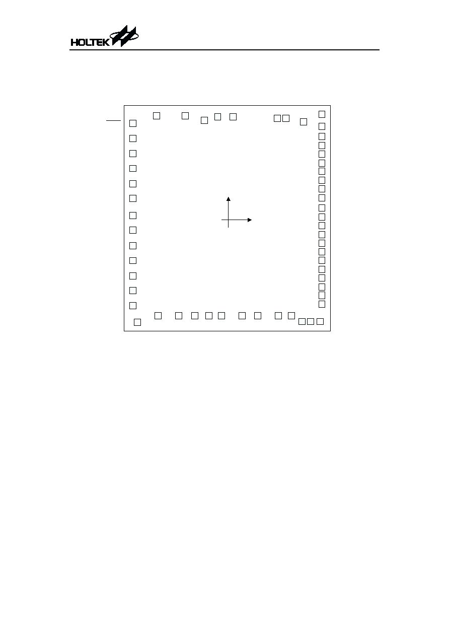
Pad Assignment
* The IC substrate should be connected to VSS in the PCB layout artwork.
HT47C20
4
January 18, 2000
M C L R
P A 0
P A 2
P A 1
P A 3
P A 4
P A 5
P A 6
P B 0
P A 7
P B 2
P B 1
P B 3
V S S
RT
1
RS
1
CS
1
IN
1
RT
0
RS
0
CRT
0
IN
0
CS
0
CO
M
0
CO
M
1
C O M 3
S E G 1 8
S E G 1 7
S E G 1 6
S E G 1 4
S E G 1 5
S E G 1 3
S E G 1 2
S E G 1 1
S E G 1 0
S E G 9
S E G 8
S E G 7
S E G 6
S E G 4
S E G 5
S E G 2
S E G 3
S E G 1
S E G 0
V 3
V 2
V1
C2
C1
OS
C
3
OS
C
4
VD
D
OS
C
2
OS
C
1
1
2 9
2
3 0
3
3 1
4
3 2
5
3 3
6
3 4
7
3 5
8
3 6
9
3 7
1 0
3 8
1 1
3 9
1 2
4 0
1 3
4 1
1 4
4 2
1 5
4 3
1 6
4 4
1 7
4 5
1 8
4 6
1 9
4 7
2 0
4 8
2 1
4 9
2 2
5 0
2 3
5 1
2 4
5 2
2 5
5 3
2 6
5 4
2 7
5 5
2 8
5 6
( 0 , 0 )
CO
M
2
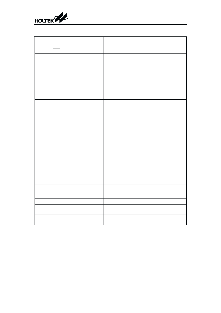
Pad Description
Pad No.
Pad Name
I/O
Mask
Option
Function
1
RES
I
¾
Schmitt trigger reset input. Active low.
2
3
4
5
6~9
PA0/BZ
PA1/BZ
PA2/IR
PA3/PFD
PA4~PA7
I/O
Wake-up
Pull-high
or None
CMOS or
NMOS
Bidirectional 8-bit input/output port. The low nibble
of the PA can be configured as CMOS output or
NMOS output with or without pull-high resistors
(mask option). NMOS output can be configured as
schmitt trigger input with or without pull-high resis-
tors. Each bit of NMOS output can be configured as
wake up input by mask option. Of the eight bits,
PA0~PA1 can be set as I/O pins or buzzer outputs by
mask option. PA2 can be set as an I/O pin or an IR
carrier output also by mask option. PA3 can be set as
an I/O pin or a PFD output also by mask option.
10
11
12
13
PB0/INT
PB1
PB2/TMR
PB3
I
¾
Four-bit Schmitt trigger input port. The PB is config-
ured as with pull-high resistors. Of the four bits, PB0
can be set as an input pin or an external interrupt in-
put pin (INT) by software application. While PB2 can
be set as an input pin or a timer/event counter input
pin also by software application.
14
VSS
¾
¾
Negative power supply, GND
18
17
16
15
IN1
CS1
RS1
RT1
I
O
O
O
¾
Oscillation input pin of channel 1
Reference capacitor connection pin of channel 1
Reference resistor connection pin of channel 1
Resistor sensor connection pin for measurement of
channel 1
23
22
21
20
19
IN0
CS0
RS0
CRT0
RT0
I
O
O
O
O
¾
Oscillation input pin of channel 0
Reference capacitor connection pin of channel 0
Reference resistor connection pin of channel 0
Resistor/capacitor sensor connection pin for mea-
surement of channel 0
Resistor sensor connection pin for measurement of
channel 0
27
26~24
SEG19/COM3
COM2~COM0
O
1/3 or 1/4
Duty
SEG19/COM3 can be set as a segment or a common
output driver for LCD panel by mask option.
COM2~COM0 are outputs for LCD panel plate.
28~46
SEG18~SEG0
O
¾
LCD driver outputs for LCD panel segments
49, 48, 47
51, 50
V1, V2, V3
C1, C2
¾
¾
Voltage pump
52
53
OSC4
OSC3
O
I
¾
Real time clock oscillators
HT47C20
5
January 18, 2000
Document Outline
- þÿ
- þÿ
- þÿ
- þÿ
- þÿ
- þÿ
- þÿ
- þÿ
- þÿ
- þÿ
- þÿ
- þÿ
- þÿ