 | ÐлекÑÑоннÑй компоненÑ: HT47C20L | СкаÑаÑÑ:  PDF PDF  ZIP ZIP |
Äîêóìåíòàöèÿ è îïèñàíèÿ www.docs.chipfind.ru

HT47C20L
8-Bit Microcontroller
1
January 18, 2000
Features
·
Operating voltage: 1.2V~2.2V
·
Eight bidirectional I/O lines
·
Four input lines
·
One interrupt input
·
One 16-bit programmable timer/event
counter with PFD (programmable
frequency divider) function
·
On-chip 32768Hz crystal oscillator
·
Watchdog timer
·
2K ´ 16 program memory ROM
·
64 ´ 8 data memory RAM
·
One real time clock (RTC)
·
One 8-bit prescaler for real time clock
·
One buzzer output
·
One low voltage detector
·
One low voltage reset circuit
·
Halt function and wake-up feature reduce
power consumption
·
LCD bias C type
·
One LCD driver with 20 ´ 2 or 20 ´ 3 or 19 ´ 4
segments
·
Two channels RC type A/D converter
·
Four-level subroutine nesting
·
Bit manipulation instruction
·
16-bit table read instruction
·
Up to 122ms instruction cycle with 32768Hz
system clock
·
All instructions in one or two machine cycles
·
63 powerful instructions
General Description
The HT47C20L is an 8-bit high performance
RISC-like microcontroller. Its single cycle in-
struction and two-stage pipeline architecture
make high speed applications. The device is
suited for use in multiple LCD low power appli-
cations among which are calculators, clock tim-
ers, games, scales, toys, thermometers,
hygrometers, body thermometers, capacitor
scaler, other hand held LCD products, and bat-
tery system in particular.
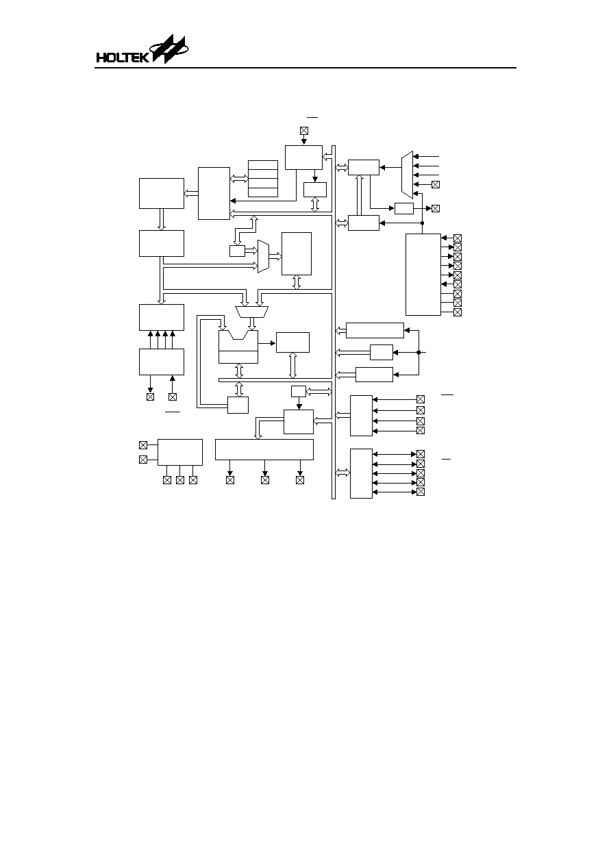
Block Diagram
HT47C20L
2
January 18, 2000
P B 0 / I N T
P r o g r a m
C o u n t e r
P r o g r a m
R O M
I n s t r u c t i o n
R e g i s t e r
I n s t r u c t i o n
D e c o d e r
T i m i n g
G e n e r a t o r
O S C 2
O S C 1
R E S
V D D
V S S
I n t e r r u p t
C i r c u i t
I N T C
M P
M
U
X
M U X
D A T A
M e m o r y
A L U
S h i f t e r
S T A T U S
A C C
P A
P o r t A
P A 0 / B Z
T i m e r A
M
U
X
3 2 7 6 8 H z
( a l w a y s o n )
P B
P o r t B
P B 2 / T M R
P A 2
P A 3 / P F D
P A 4 ~ P A 7
P A 1 / B Z
P B 1
P B 3
P B 0 / I N T
R e a l T i m e C l o c k
L C D
M e m o r y
B P
L C D D r i v e r
C O M 0 ~
C O M 2
C O M 3 /
S E G 1 9
S E G 0 ~
S E G 1 8
T i m e B a s e
W D T
T i m e r B
S y s t e m C l o c k
T 1
R T C O u t p u t
P B 2 / T M R
P F D
I N 0
C S 0
R S 0
C R T 0
R T 0
I N 1
C S 1
R S 1
R T 1
R C
T y p e
A / D
C o n v e r t e r
A / D C l o c k
P B 3 / P F D
D o u b l e
V o l t a g e
C 1
C 2
V 1 V 2 V 3
S T A C K 0
S T A C K 1
S T A C K 2
S T A C K 3
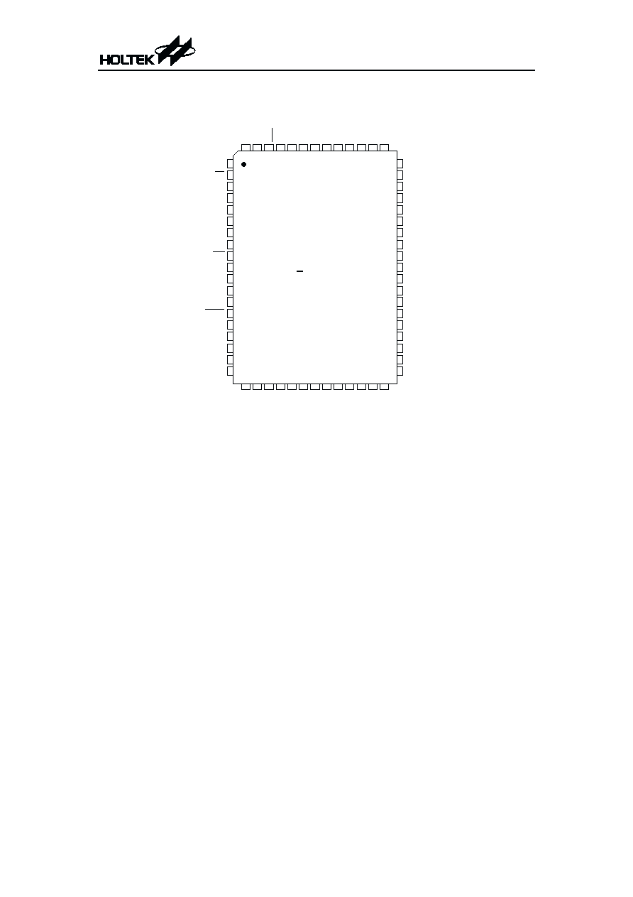
Pin Assignment
HT47C20L
3
January 18, 2000
2 0 2 1 2 2 2 3 2 4 2 5 2 6 2 7 2 8 2 9 3 0 3 1 3 2
1
2
3
4
5
6
7
8
9
1 0
1 1
1 2
1 3
1 4
1 5
1 6
1 7
1 8
1 9
5 1
5 0
4 9
4 8
4 7
4 6
4 5
4 4
4 3
4 2
4 1
4 0
3 9
3 8
3 7
3 6
3 5
3 4
3 3
6 1 6 0 5 9 5 8 5 7 5 6 5 5 5 4 5 3 5 2
6 4 6 3 6 2
RT
1
RS
1
CS
1
IN
1
CRT
0
RT
0
RS
0
CS
0
IN
0
CO
M
0
CO
M
1
CO
M
2
CO
M
3
/
S
E
G
1
9
V3
V2
V1
C2
C1
NC
NC
VD
D
OS
C
2
OS
C
1
NC
RE
S
NC
S E G 0
S E G 1
S E G 2
S E G 3
S E G 4
S E G 5
S E G 6
S E G 7
S E G 8
S E G 9
S E G 1 0
S E G 1 1
S E G 1 2
S E G 1 3
S E G 1 4
S E G 1 5
S E G 1 6
S E G 1 7
S E G 1 8
P A 0 / B Z
P A 1 / B Z
P A 2
P A 3 / P F D
P A 4
P A 5
P A 6
P A 7
P B 0 / I N T
P B 1
P B 2 / T M R
P B 3
N C
T E S T
N C
N C
N C
N C
V S S
H T 4 7 C 2 0 L
6 4 Q F P
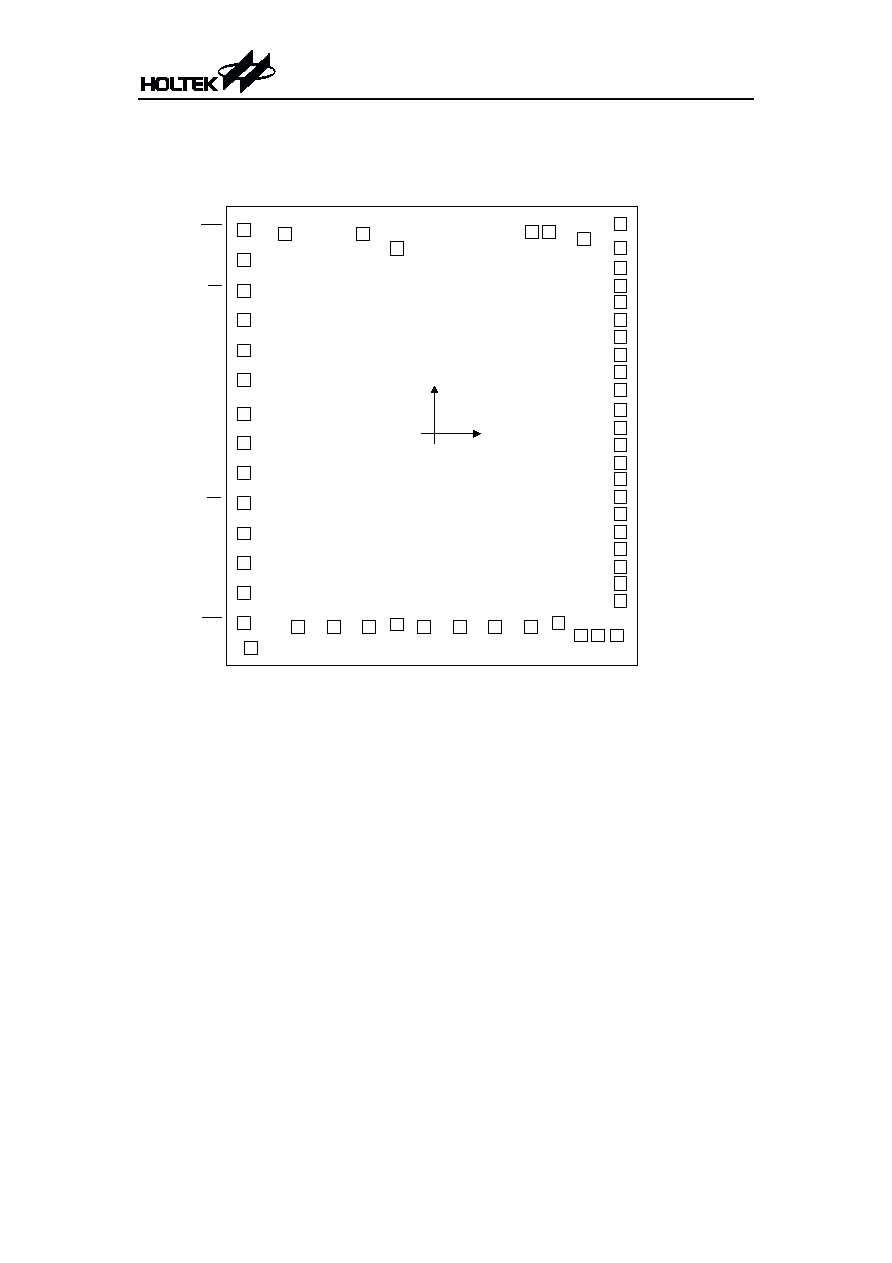
Pad Assignment
* The IC substrate should be connected to VSS in the PCB layout artwork.
HT47C20L
4
January 18, 2000
P B 0 / I N T
P A 1 / B Z
R E S
T E S T
1
2 9
2
3 0
3
3 1
4
3 2
5
3 3
6
3 4
7
3 5
8
3 6
9
3 7
1 0
3 8
1 1
3 9
1 2
4 0
1 3
4 1
1 4
4 2
1 5
4 3
1 6
4 4
1 7
4 5
1 8
4 6
1 9
4 7
2 0
4 8
2 1
4 9
2 2
5 0
2 3
5 1
2 4
5 2
2 5
5 3
2 6
5 4
2 7
5 5
2 8
( 0 , 0 )
P A 0 / B Z
P A 3 / P F D
P A 2
P A 5
P A 7
P A 6
P A 4
P B 1
P B 2 / T M R
P B 3
V S S
RT
1
RS
1
IN
1
CS
1
RT
0
CRT
0
RS
0
CS
0
IN
0
CO
M
0
CO
M
1
CO
M
2
C O M 3 / S E G 1 9
S E G 1 8
S E G 1 7
S E G 1 6
S E G 1 5
S E G 1 4
S E G 1 3
S E G 1 2
S E G 1 1
S E G 1 0
S E G 9
S E G 8
S E G 7
S E G 6
S E G 5
S E G 4
S E G 3
S E G 2
S E G 1
S E G 0
V 3
V 2
V1
C2
C1
VD
D
OS
C
2
OS
C
1
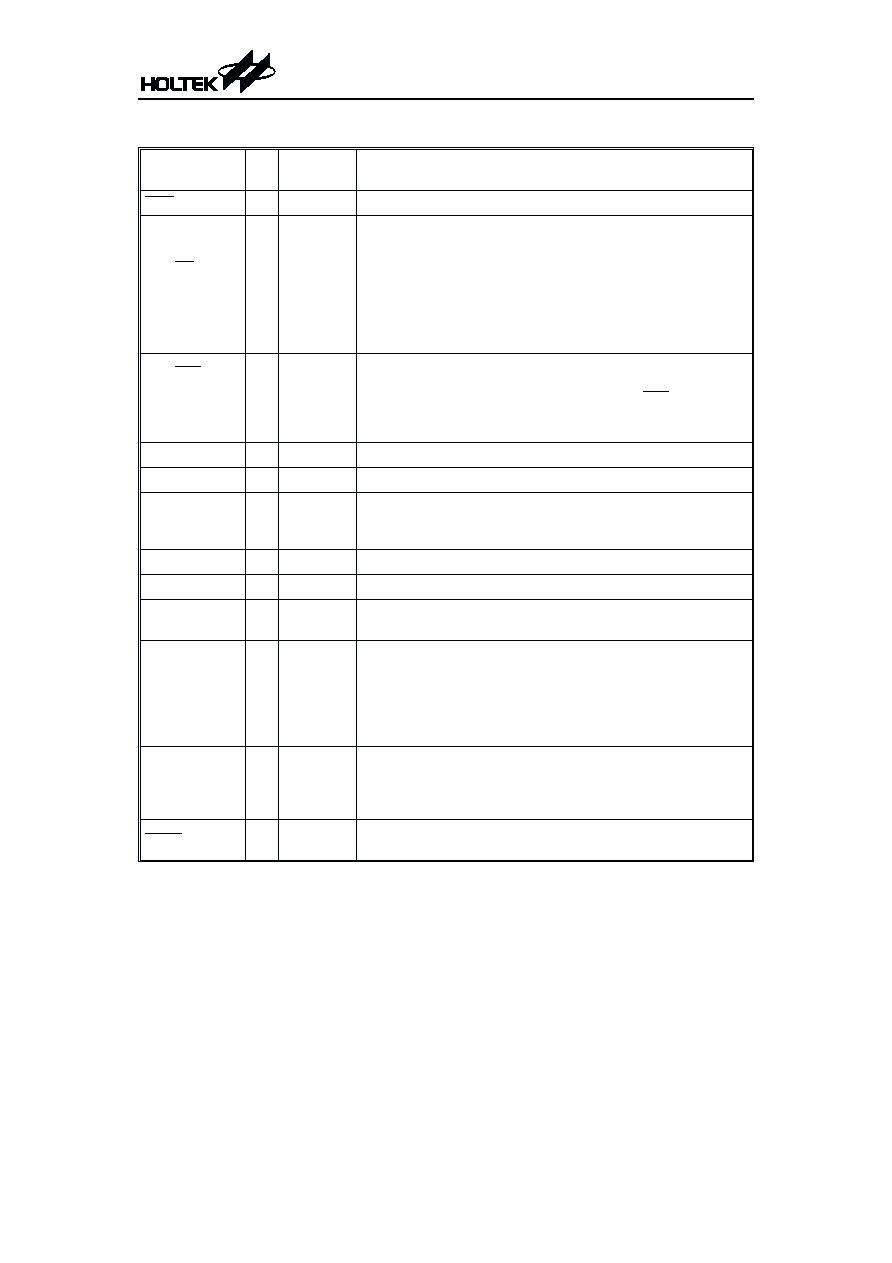
Pin Description
Pin Name
I/O
Mask
Option
Function
RES
I
¾
Schmitt trigger reset input. Active low.
PA0/BZ
PA1/BZ
PA2
PA3/PFD
PA4~PA7
I/O
Wake-up
Pull-high
or None
CMOS or
NMOS
Bidirectional 8-bit input/output port. The low nibble of the PA
can be configured as CMOS output or NMOS output with or
without pull-high resistors (mask option). NMOS output can be
configured as schmitt trigger input with or without pull-high
resistors. Each bit of NMOS output can be configured as wake
up input by mask option. Of the eight bits, PA0~PA1 can be set
as I/O pins or buzzer outputs by mask option. PA3 can be set as
an I/O pin or a PFD output by mask option.
PB0/INT
PB1
PB2/TMR
PB3
I
¾
Four-bit schmitt trigger input port. The PB is configured as
with pull-high resistors. Of the four bits, PB0 can be set as an
input pin or an external interrupt input pin (INT) by software
application. While PB2 can be set as an input pin or a
timer/event counter input pin by software application.
VSS
¾
¾
Negative power supply, GND
V1~V3, C1~C2 ¾
¾
Voltage pump
SEG19/COM3
COM2~COM0
O
1/2 or 1/3
or 1/4
Duty
SEG19/COM3 can be set as a segment or a common output
driver for LCD panel by mask option. COM2~COM0 are out-
puts for LCD panel plate.
SEG18~SEG0
O
¾
LCD driver outputs for LCD panel segments
VDD
¾
¾
Positive power supply
OSC2
OSC1
O
I
¾
OSC1 and OSC2 are connected to a 32768Hz crystal for the in-
ternal system clock and WDT source.
IN0
CS0
RS0
CRT0
RT0
I
O
O
O
O
¾
Oscillation input pin of channel 0
Reference capacitor connection pin of channel 0
Reference resistor connection pin of channel 0
Resistor/capacitor sensor connection pin for measurement of
channel 0
Resistor sensor connection pin for measurement of channel 0
IN1
CS1
RS1
RT1
I
O
O
O
¾
Oscillation input pin of channel 1
Reference capacitor connection pin of channel 1
Reference resistor connection pin of channel 1
Resistor sensor connection pin for measurement of channel 1
TEST
I
¾
TEST mode input pin with pull-high resistor.
It disconnects in normal operation.
HT47C20L
5
January 18, 2000
Document Outline
- þÿ
- þÿ
- þÿ
- þÿ
- þÿ
- þÿ
- þÿ
- þÿ
- þÿ
- þÿ
- þÿ
- þÿ
- þÿ