 | –≠–ª–µ–∫—Ç—Ä–æ–Ω–Ω—ã–π –∫–æ–º–ø–æ–Ω–µ–Ω—Ç: HT48C10-1 | –°–∫–∞—á–∞—Ç—å:  PDF PDF  ZIP ZIP |
Document Outline
- ˛ˇ
- ˛ˇ
- ˛ˇ
- ˛ˇ
- ˛ˇ
- ˛ˇ
- ˛ˇ
- ˛ˇ
- ˛ˇ
- ˛ˇ
- ˛ˇ
- ˛ˇ
- ˛ˇ
- ˛ˇ
- ˛ˇ

HT48R10A-1/HT48C10-1
I/O Type 8-Bit MCU
Rev. 1.90
1
November 4, 2005
General Description
The HT48R10A-1/HT48C10-1 are 8-bit high perfor-
mance, RISC architecture microcontroller devices spe-
cifically designed for multiple I/O control product
applications. The mask version HT48C10-1 is fully pin
and functionally compatible with the OTP version
HT48R10A-1 device.
The advantages of low power consumption, I/O flexibil-
ity, timer functions, oscillator options, HALT and
wake-up functions, watchdog timer, buzzer driver, as
well as low cost, enhance the versatility of these devices
to suit a wide range of application possibilities such as
industrial control, consumer products, subsystem con-
trollers, etc.
Features
∑
Operating voltage:
f
SYS
=4MHz: 2.2V~5.5V
f
SYS
=8MHz: 3.3V~5.5V
∑
Low voltage reset function
∑
21 bidirectional I/O lines (max.)
∑
1 interrupt input shared with an I/O line
∑
8-bit programmable timer/event counter with over-
flow interrupt and 8-stage prescaler
∑
On-chip external crystal, RC oscillator and internal
RC oscillator
∑
32768Hz crystal oscillator for timing purposes only
∑
Watchdog Timer
∑
1024
¥14 program memory ROM
∑
64
¥8 data memory RAM
∑
Buzzer driving pair and PFD supported
∑
HALT function and wake-up feature reduce power
consumption
∑
Up to 0.5
ms instruction cycle with 8MHz system clock
at V
DD
=5V
∑
All instructions in one or two machine cycles
∑
14-bit table read instruction
∑
4-level subroutine nesting
∑
Bit manipulation instruction
∑
63 powerful instructions
∑
24-pin SKDIP/SOP package
Technical Document
∑
Tools Information
∑
FAQs
∑
Application Note
-
HA0003E Communicating between the HT48 & HT46 Series MCUs and the HT93LC46 EEPROM
-
HA0004E HT48 & HT46 MCU UART Software Implementation Method
-
HA0013E HT48 & HT46 LCM Interface Design
-
HA0021E Using the I/O Ports on the HT48 MCU Series
-
HA0055E 2^12 Decoder (8+4 - Corresponds to HT12E)

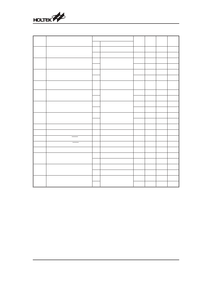
Block Diagram
Pin Assignment
HT48R10A-1/HT48C10-1
Rev. 1.90
2
November 4, 2005
I N T / P C 0
O S C 2 /
P C 4
O S C 1 /
P C 3
R E S
V D D
M U X
P A C
P A
P O R T A
P A 0 ~ P A 7
T M R / P C 1
f
S Y S
/ 4
W D T S
W D T
P C C
P C
P O R T C
P C 0 ~ P C 4
P B C
P B
P O R T B
P B 0 ~ P B 7
T M R
V S S
P r e s c a l e r
f
S Y S
B Z / B Z
P C 0
P C 1
P r o g r a m
R O M
P r o g r a m
C o u n t e r
I n t e r r u p t
C i r c u i t
S T A C K
I N T C
D A T A
M e m o r y
I n s t r u c t i o n
R e g i s t e r
M
U
X
I n s t r u c t i o n
D e c o d e r
S T A T U S
A L U
S h i f t e r
T i m i n g
G e n e r a t o r
A C C
W D T O S C
W D T P r e s c a l e r
M
U
X
M
U
X
M P
M
U
X
R T C O S C
E N / D I S
P C 3
P C 4
I n t e r n a l
R C O S C
T M R C
2 4
2 3
2 2
2 1
2 0
1 9
1 8
1 7
1 6
1 5
1 4
1 3
1
2
3
4
5
6
7
8
9
1 0
1 1
1 2
H T 4 8 R 1 0 A - 1 / H T 4 8 C 1 0 - 1
2 4 S K D I P - A / S O P - A
P B 6
P B 7
P A 4
P A 5
P A 6
P A 7
O S C 2 / P C 4
O S C 1 / P C 3
V D D
R E S
P C 2
P C 1 / T M R
P B 5
P B 4
P A 3
P A 2
P A 1
P A 0
P B 3
P B 2
P B 1 / B Z
P B 0 / B Z
V S S
P C 0 / I N T

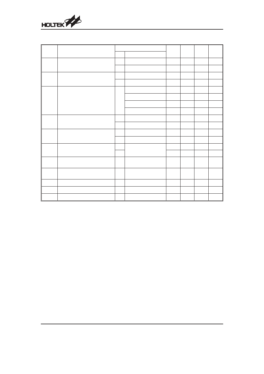
Pin Description
Pin Name
I/O
Options
Description
PA0~PA7
I/O
Pull-high*
Wake-up
CMOS/Schmitt
trigger Input
Bidirectional 8-bit input/output port. Each bit can be configured as wake-up input
by options. Software instructions determine the CMOS output or Schmitt trigger
or CMOS (dependent on options) input with a pull-high resistor (determined by
pull-high options).
PB0/BZ
PB1/BZ
PB2~PB7
I/O
Pull-high*
I/O or BZ/BZ
Bidirectional 8-bit input/output port. Software instructions determine the CMOS
output or Schmitt trigger input with a pull-high resistor (determined by pull-high
options).
The PB0 and PB1 are pin-shared with the BZ and BZ, respectively. Once the PB0
and PB1 are selected as buzzer driving outputs, the output signals come from an
internal PFD generator (shared with timer/event counter).
VSS
æ
æ
Negative power supply, ground
PC0/INT
PC1/TMR
PC2
I/O
Pull-high*
Bidirectional I/O lines. Software instructions determine the CMOS output or
Schmitt trigger input with a pull-high resistor (determined by pull-high options).
The external interrupt and timer input are pin-shared with the PC0 and PC1, re-
spectively. The external interrupt input is activated on a high to low transition.
RES
I
æ
Schmitt trigger reset input. Active low
VDD
æ
æ
Positive power supply
OSC1/PC3
OSC2/PC4
I
O
Crystal or RC
or Int. RC+I/O
or Int. RC+RTC
OSC1, OSC2 are connected to an RC network or Crystal (determined by options)
for the internal system clock. In the case of RC operation, OSC2 is the output ter-
minal for 1/4 system clock. These two pins also can be optioned as an RTC oscil-
lator (32768Hz) or I/O lines. In these two cases, the system clock comes from an
internal RC oscillator whose frequency has 4 options (3.2MHz, 1.6MHz, 800kHz,
400kHz). If the I/O option is selected, the pull-high options also be enabled. Oth-
erwise the PC3 and PC4 are used as internal registers (pull-high resistors always
disabled).
* The pull-high resistors of each I/O port (PA, PB, PC) are controlled by an option bit.
Absolute Maximum Ratings
Supply Voltage ...........................V
SS
-0.3V to V
SS
+6.0V
Storage Temperature ............................
-50∞C to 125∞C
Input Voltage..............................V
SS
-0.3V to V
DD
+0.3V
Operating Temperature...........................
-40∞C to 85∞C
Note: These are stress ratings only. Stresses exceeding the range specified under
≤Absolute Maximum Ratings≤ may
cause substantial damage to the device. Functional operation of this device at other conditions beyond those
listed in the specification is not implied and prolonged exposure to extreme conditions may affect device reliabil-
ity.
HT48R10A-1/HT48C10-1
Rev. 1.90
3
November 4, 2005
D.C. Characteristics
Ta=25
∞C
Symbol
Parameter
Test Conditions
Min.
Typ.
Max.
Unit
V
DD
Conditions
V
DD
Operating Voltage
æ f
SYS
=4MHz
2.2
æ
5.5
V
æ f
SYS
=8MHz
3.3
æ
5.5
V
I
DD1
Operating Current (Crystal OSC)
3V
No load, f
SYS
=4MHz
æ
0.6
1.5
mA
5V
æ
2
4
mA
I
DD2
Operating Current (RC OSC)
3V
No load, f
SYS
=4MHz
æ
0.8
1.5
mA
5V
æ
2.5
4
mA
I
DD3
Operating Current
(Crystal OSC, RC OSC)
5V
No load, f
SYS
=8MHz
æ
4
8
mA
I
STB1
Standby Current
(WDT Enabled RTC Off)
3V
No load, system HALT
æ
æ
5
mA
5V
æ
æ
10
mA
I
STB2
Standby Current
(WDT Disabled RTC Off)
3V
No load, system HALT
æ
æ
1
mA
5V
æ
æ
2
mA
I
STB3
Standby Current
(WDT Disabled, RTC On)
3V
No load, system HALT
æ
æ
5
mA
5V
æ
æ
10
mA
V
IL1
Input Low Voltage for I/O Ports
æ
æ
0
æ
0.3V
DD
V
V
IH1
Input High Voltage for I/O Ports
æ
æ
0.7V
DD
æ
V
DD
V
V
IL2
Input Low Voltage (RES)
æ
æ
0
æ
0.4V
DD
V
V
IH2
Input High Voltage (RES)
æ
æ
0.9V
DD
æ
V
DD
V
V
LVR
Low Voltage Reset
æ LVRenabled
2.7
3.0
3.3
V
I
OL
I/O Port Sink Current
3V
V
OL
=0.1V
DD
4
8
æ
mA
5V
V
OL
=0.1V
DD
10
20
æ
mA
I
OH
I/O Port Source Current
3V
V
OH
=0.9V
DD
-2
-4
æ
mA
5V
V
OH
=0.9V
DD
-5
-10
æ
mA
R
PH
Pull-high Resistance
3V
æ
20
60
100
k
W
5V
10
30
50
k
W
HT48R10A-1/HT48C10-1
Rev. 1.90
4
November 4, 2005
A.C. Characteristics
Ta=25
∞C
Symbol
Parameter
Test Conditions
Min.
Typ.
Max.
Unit
V
DD
Conditions
f
SYS1
System Clock (Crystal OSC)
æ 2.2V~5.5V
400
æ
4000
kHz
æ 3.3V~5.5V
400
æ
8000
kHz
f
SYS2
System Clock (RC OSC)
æ 2.2V~5.5V
400
æ
4000
kHz
æ 3.3V~5.5V
400
æ
8000
kHz
f
SYS3
System Clock (Internal RC OSC)
5V
3.2MHz
1800
æ
5400
kHz
1.6MHz
900
æ
2700
kHz
800kHz
450
æ
1350
kHz
400kHz
225
æ
675
kHz
f
TIMER
Timer I/P Frequency (TMR)
æ 2.2V~5.5V
0
æ
4000
kHz
æ 3.3V~5.5V
0
æ
8000
kHz
t
WDTOSC
Watchdog Oscillator Period
3V
æ
45
90
180
ms
5V
æ
32
65
130
ms
t
WDT1
Watchdog Time-out Period
(WDT OSC)
3V
Without WDT prescaler
11
23
46
ms
5V
8
17
33
ms
t
WDT2
Watchdog Time-out Period
(System Clock)
æ Without WDT prescaler
æ
1024
æ
t
SYS
t
WDT3
Watchdog Time-out Period
(RTC OSC)
æ Without WDT prescaler
æ
7.812
æ
ms
t
RES
External Reset Low Pulse Width
æ
æ
1
æ
æ
ms
t
SST
System Start-up Timer Period
æ Wake-up from HALT
æ
1024
æ
t
SYS
t
INT
Interrupt Pulse Width
æ
æ
1
æ
æ
ms
HT48R10A-1/HT48C10-1
Rev. 1.90
5
November 4, 2005