 | ÐлекÑÑоннÑй компоненÑ: HT48CA6 | СкаÑаÑÑ:  PDF PDF  ZIP ZIP |
Äîêóìåíòàöèÿ è îïèñàíèÿ www.docs.chipfind.ru
HT48CA6
8-Bit Remote Type Low Voltage Mask MCU
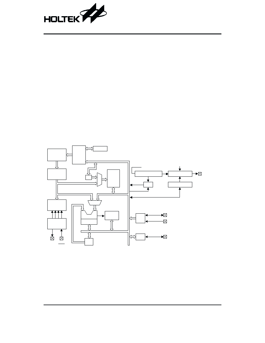
Block Diagram
Rev. 1.10
1
July 26, 2002
Features
·
Operating voltage: 1.8V~3.6V
·
Ten bidirectional I/O lines
·
Six Schmitt trigger input lines
·
One carrier output, 1/2 or 1/3 duty with high sink cur-
rent capability
·
On-chip crystal and RC oscillator
·
Watchdog Timer
·
1K
´14 program ROM
·
32
´8 data RAM
·
HALT function and wake-up feature reduce power
consumption
·
62 powerful instructions
·
Up to 1
ms instruction cycle with 4MHz system clock
·
All instructions in 1 or 2 machine cycles
·
14-bit table read instructions
·
One-level subroutine nesting
·
Bit manipulation instructions
·
20/24-pin SOP package
General Description
The HT48CA6 is an 8-bit high performance RISC-like
microcontroller specifically designed for multiple I/O
product applications. The device is particularly suitable
for use in products such as remote controllers, toys and
various subsystem controllers. A HALT feature is in-
cluded to reduce power consumption.
P r o g r a m
C o u n t e r
P r o g r a m
R O M
I n s t r u c t i o n
R e g i s t e r
I n s t r u c t i o n
D e c o d e r
T i m i n g
G e n e r a t o r
O S C 2
O S C 1
R E S
V D D
V S S
M P
M
U
X
M U X
D A T A
M e m o r y
A L U
S h i f t e r
S T A T U S
A C C
P A
P O R T A
P A 0 ~ P A 7
S Y S C L K / 4
W D T
. r e q u e n c y D i v i d e r
P B
P B 2 ~ P B 7
S T A C K
C a r r i e r C o n t r o l
L e v e l o r C a r r i e r
P C 0 / R E M
P C 0 C o n t r o l
P O R T B
P B 0 ~ P B 1
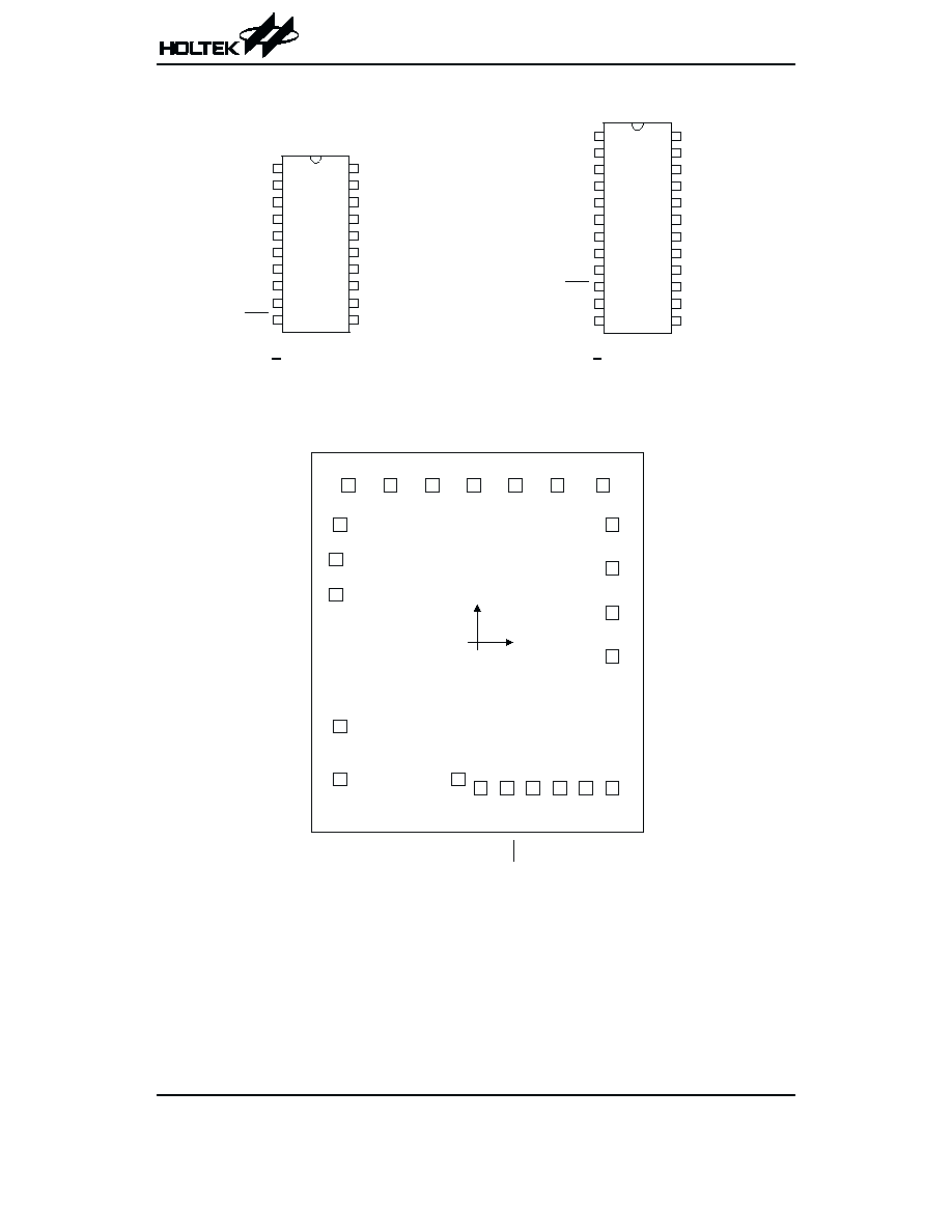
Pin Assignment
Pad Assignment
* The IC substrate should be connected to VSS in the PCB layout artwork.
HT48CA6
Rev. 1.10
2
July 26, 2002
P A 1
P A 0
P B 1
P B 0
V D D
O S C 1
O S C 2
P C 0 / R E M
V S S
R E S
P A 2
P A 3
P A 4
P A 5
P A 6
P A 7
P B 2
P B 3
P B 4
P B 5
P B 6
P B 7
P A 1
P A 0
P B 1
P B 0
V D D
O S C 1
O S C 2
P C 0 / R E M
V S S
R E S
N C
N C
2 4
2 3
2 2
2 1
2 0
1 9
1 8
1 7
1 6
1 5
1 4
1 3
1
2
3
4
5
6
7
8
9
1 0
1 1
1 2
1
2
3
4
5
6
7
8
9
1 0
P A 2
P A 3
P A 4
P A 5
P A 6
P A 7
P B 2
P B 3
P B 4
P B 5
2 0
1 9
1 8
1 7
1 6
1 5
1 4
1 3
1 2
1 1
H T 4 8 C A 6
2 4 S O P - A
H T 4 8 C A 6
2 0 S O P - A
P B 3
P B 2
P A 7
P A 6
V
S
S
P
B
7
P
B
6
P
B
5
P
B
4
O S C 1
O S C 2
V D D
P B 0
P
B
1
P
A
0
P
A
1
P
A
2
P
A
3
P
A
4
P
A
5
R
E
S
( 0 , 0 )
1
2
3
4
5
6
7
8
9
1 0
1 1
1 2
1 3
1 8
1 7
1 6
1 5
1 4
2 3
2 2
2 1
2 0
1 9
P C 0
V
S
S
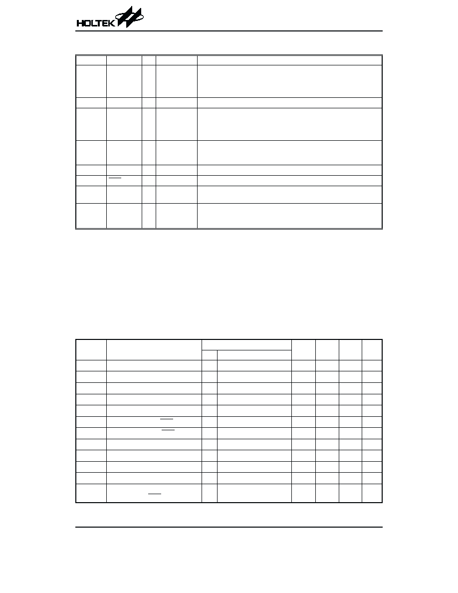
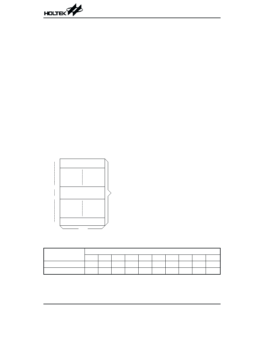
Pad Description
Pad No.
Pad Name
I/O
Mask Option
Description
2, 1
PB0, PB1
I/O
Wake-up
or None
2-bit bidirectional input/output lines with pull-high resistors. Each bit
can be determined as NMOS output or Schmitt trigger input by soft-
ware instructions. Each bit can also be configured as wake-up input
by mask option.
3
VDD
¾
¾
Positive power supply
4
5
OSC1
OSC2
I
O
Crystal or RC
OSC1, OSC2 are connected to an RC network or a crystal (deter-
mined by mask option) for the internal system clock. In the case of RC
operation, OSC2 is the output terminal for 1/4 system clock (NMOS
open drain output).
6
PC0/REM
O
Level or
Carrier
Level or carrier output pin
PC0 can be set as CMOS level output pin or carrier output pin by
mask option.
7, 8
VSS
¾
¾
Negative power supply, ground
9
RES
I
¾
Schmitt trigger reset input. Active low.
15~10
PB2~PB7
I
Wake-up
or None
6-bit Schmitt trigger input lines with pull-high resistors. Each bit can
be configured as a wake-up input by mask option.
23~16
PA0~PA7
I/O
¾
Bidirectional 8-bit input/output port with pull-high resistors. Each bit
can be determined as NMOS output or Schmitt trigger input by soft-
ware instructions.
Absolute Maximum Ratings
Supply Voltage ............................................
-0.3V to 4V
Storage Temperature ............................
-50°C to 125°C
Input Voltage..............................V
SS
-0.3V to V
DD
+0.3V
Operating Temperature...........................
-25°C to 70°C
Note: These are stress ratings only. Stresses exceeding the range specified under
²Absolute Maximum Ratings² may
cause substantial damage to the device. Functional operation of this device at other conditions beyond those
listed in the specification is not implied and prolonged exposure to extreme conditions may affect device reliabil-
ity.
D.C. Characteristics
Ta=25
°C
Symbol
Parameter
Test Conditions
Min.
Typ.
Max.
Unit
V
DD
Conditions
V
DD
Operating Voltage
¾ f
SYS
=4MHz
1.8
¾
3.6
V
I
DD
Operating Current
3V
No load, f
SYS
=4MHz
¾
0.7
1.5
mA
I
STB
Standby Current
3V
No load, system HALT
¾
¾
1
mA
V
IL1
Input Low Voltage for I/O Ports
3V
¾
0
¾
1.05
V
V
IH1
Input High Voltage for I/O Ports
3V
¾
1.95
¾
3
V
V
IL2
Input Low Voltage (RES)
3V
¾
¾
1.5
¾
V
V
IH2
Input High Voltage (RES)
3V
¾
¾
2.4
¾
V
I
OL1
PC0/REM Sink Current
3V
V
OL
=0.3V
100
150
¾
mA
I
OL2
PC0/REM Sink Current
3V
V
OL
=0.6V
200
300
¾
mA
I
OH1
PC0/REM Source Current
3V
V
OH
=2.7V
-1
-2
¾
mA
I
OL3
Sink Current of I/O Line
3V
V
OL
=0.3V
1.5
2.5
¾
mA
R
PH
Pull-high Resistance of PA Port,
PB0~PB7 and RES
3V
¾
20
40
¾
k
W
HT48CA6
Rev. 1.10
3
July 26, 2002
A.C. Characteristics
Ta=25
°C
Symbol
Parameter
Test Conditions
Min.
Typ.
Max.
Unit
V
DD
Conditions
f
SYS
System Clock
3V
¾
400
¾
4000
kHz
t
RES
External Reset Low Pulse Width
¾
¾
1
¾
¾
ms
t
SST
System Start-up timer Period
¾
Power-up or wake-up
from HALT
¾
1024
¾
t
SYS
Note: t
SYS
=1/f
SYS
HT48CA6
Rev. 1.10
4
July 26, 2002
Functional Description
Execution flow
The HT48CA6 system clock can be derived from a crys-
tal/ceramic resonator oscillator. It is internally divided
into four non-overlapping clocks. One instruction cycle
consists of four system clock cycles.
Instruction fetching and execution are pipelined in such
a way that a fetch takes one instruction cycle while de-
coding and execution takes the next instruction cycle.
However, the pipelining scheme causes each instruc-
tion to effectively execute within 1 cycle. If an instruction
changes the program counter, two cycles are required to
complete the instruction.
Program counter
- PC
The 10-bit program counter (PC) controls the sequence
in which the instructions stored in program ROM are ex-
ecuted and its contents specify a maximum of 1024 ad-
dresses.
After accessing a program memory word to fetch an in-
struction code, the contents of the program counter are
incremented by 1. The program counter then points to
the memory word containing the next instruction code.
When executing a jump instruction, conditional skip ex-
ecution, loading PCL register, subroutine call, initial re-
set or return from subroutine, the PC manipulates the
program transfer by loading the address corresponding
to each instruction.
The conditional skip is activated by instruction. Once the
condition is met, the next instruction, fetched during the
current instruction execution, is discarded and a dummy
cycle replaces it to get the proper instruction. Otherwise
proceed with the next instruction.
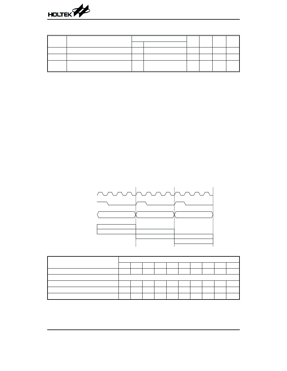
T 1
T 2
T 3
T 4
T 1
T 2
T 3
T 4
T 1
T 2
T 3
T 4
. e t c h I N S T ( P C )
E x e c u t e I N S T ( P C - 1 )
. e t c h I N S T ( P C + 1 )
E x e c u t e I N S T ( P C )
. e t c h I N S T ( P C + 2 )
E x e c u t e I N S T ( P C + 1 )
P C
P C + 1
P C + 2
S y s t e m C l o c k
I n s t r u c t i o n C y c l e
P C
Execution flow
Mode
Program Counter
*9
*8
*7
*6
*5
*4
*3
*2
*1
*0
Initial reset
0
0
0
0
0
0
0
0
0
0
Skip
PC+2
Loading PCL
*9
*8
@7
@6
@5
@4
@3
@2
@1
@0
Jump, call branch
#9
#8
#7
#6
#5
#4
#3
#2
#1
#0
Return from subroutine
S9
S8
S7
S6
S5
S4
S3
S2
S1
S0
Program counter
Note: *9~*0: Program counter bits
S9~S0: Stack register bits
#9~#0: Instruction code bits
@7~@0: PCL bits
HT48CA6
Rev. 1.10
5
July 26, 2002
The lower byte of the program counter (PCL) is a read-
able and writeable register (06H). Moving data into the
PCL performs a short jump. The destination will be
within 256 locations.
When a control transfer takes place, an additional
dummy cycle is required.
Program memory
- ROM
The program memory is used to store the program in-
structions which are to be executed. It also contains
data and table and is organized into 1024
´14 bits, ad-
dressed by the program counter and table pointer.
Certain locations in the program memory are reserved
for special usage:
·
Location 000H
This area is reserved for the initialization program. Af-
ter chip reset, the program always begins execution at
location 000H.
·
Table location
Any location in the ROM space can be used as
look-up tables. The instructions TABRDC [m] (the cur-
rent page, 1 page=256 words) and TABRDL [m] (the
last page) transfer the contents of the lower-order byte
to the specified data memory, and the higher-order
byte to TBLH (08H). Only the destination of the
lower-order byte in the table is well-defined, the other
bits of the table word are transferred to the lower por-
tion of TBLH, the remaining 2 bits are read as
²0². The
Table Higher-order byte register (TBLH) is read only.
The table pointer (TBLP) is a read/write register
(07H), where P indicates the table location. Before ac-
cessing the table, the location must be placed in
TBLP. The TBLH is read only and cannot be restored.
All table related instructions need 2 cycles to complete
the operation. These areas may function as normal
program memory depending upon the requirements.
Stack register
- STACK
This is a special part of the memory used to save the
contents of the program counter (PC) only. The stack is
organized into one level and is neither part of the data
nor part of the program space, and is neither readable
nor writeable. The activated level is indexed by the stack
pointer (SP) and is neither readable nor writeable. At a
subroutine call the contents of the program counter are
pushed onto the stack. At the end of a subroutine sig-
naled by a return instruction (RET), the program counter
is restored to its previous value from the stack. After a
chip reset, the SP will point to the top of the stack.
If the stack is full and a
²CALL² is subsequently exe-
cuted, stack overflow occurs and the first entry will be
lost (only the most recent return address is stored).
Data memory
- RAM
The data memory is designed with 42
´8 bits. The data
memory is divided into two functional groups: special
function registers and general purpose data memory
(32
´8). Most of them are read/write, but some are read
only.
The special function registers include the indirect address-
ing register (00H), the memory pointer register (MP;01H),
the accumulator (ACC;05H) the program counter
lower-order byte register (PCL;06H), the table pointer
(TBLP;07H), the table higher-order byte register
(TBLH;08H), the status register (STATUS;0AH) and the
I/O registers (PA;12H, PB;14H, PC;16H). The remaining
space before the 20H is reserved for future expanded us-
age and reading these locations will return the result 00H.
The general purpose data memory, addressed from 20H
to 3FH, is used for data and control information under in-
struction command.
Instruction(s)
Table Location
*9
*8
*7
*6
*5
*4
*3
*2
*1
*0
TABRDC [m]
P9
P8
@7
@6
@5
@4
@3
@2
@1
@0
TABRDL [m]
1
1
@7
@6
@5
@4
@3
@2
@1
@0
Table location
Note: *9~*0: Table location bits
P9~P8: Current program counter bits
@7~@0: Table pointer bits
0 0 0 H
D e v i c e i n i t i a l i z a t i o n p r o g r a m
P r o g r a m
R O M
1 4 b i t s
L o o k - u p t a b l e ( 2 5 6 w o r d s )
n 0 0 H
L o o k - u p t a b l e ( 2 5 6 w o r d s )
3 . . H
N o t e : n r a n g e s f r o m 0 t o 3
n . . H
Program memory
Document Outline
- þÿ
- þÿ
- þÿ
- þÿ
- þÿ
- þÿ
- þÿ
- þÿ
- þÿ
- þÿ
- þÿ
- þÿ
- þÿ
- þÿ
- þÿ
- þÿ