 | ÐлекÑÑоннÑй компоненÑ: HT48CU80 | СкаÑаÑÑ:  PDF PDF  ZIP ZIP |
Äîêóìåíòàöèÿ è îïèñàíèÿ www.docs.chipfind.ru

HT48RU80/HT48CU80
I/O Type 8-Bit MCU
Rev. 1.00
1
April 12, 2006
General Description
The HT48RU80/HT48CU80 are 8-bit high performance,
RISC architecture microcontroller devices specifically
designed for multiple I/O control product applications.
The mask version HT48CU80 is fully pin and function-
ally compatible with the OTP version HT48RU80 de-
vice.
The advantages of low power consumption, I/O flexibil-
ity, timer functions, oscillator options, HALT and
wake-up functions, watchdog timer, buzzer driver, as
well as low cost, enhance the versatility of these devices
to suit a wide range of application possibilities such as
industrial control, consumer products, subsystem con-
trollers, etc.
The HT48CU80 is under development and will be avail-
able soon.
Features
·
Operating voltage:
f
SYS
=4MHz: 2.2V~5.5V
f
SYS
=8MHz: 3.3V~5.5V
·
Low voltage reset function
·
56 bidirectional I/O lines (max.)
·
Two interrupt input
·
16-bit
´2 programmable timer/event counter and
overflow interrupts with PFD outputs
·
8-bit
´1 programmable timer/event counter
·
On-chip RC oscillator, external crystal and RC oscil-
lator
·
32768Hz crystal oscillator for timing purposes only
·
Watchdog Timer
·
16K
´16 program memory ROM
·
576
´8 data memory RAM
·
Universal Asynchronous Receiver/Transmitter
(UART)
·
HALT function and wake-up feature reduce power
consumption
·
16-level subroutine nesting
·
Up to 0.5
ms instruction cycle with 8MHz system clock
at V
DD
=5V
·
Bit manipulation instruction
·
16-bit table read instruction
·
63 powerful instructions
·
All instructions in one or two machine cycles
·
48-pin SSOP, 64-pin QFP package
Technical Document
·
Tools Information
·
FAQs
·
Application Note
-
HA0003E Communicating between the HT48 & HT46 Series MCUs and the HT93LC46 EEPROM
-
HA0004E HT48 & HT46 MCU UART Software Implementation Method
-
HA0013E HT48 & HT46 LCM Interface Design
-
HA0021E Using the I/O Ports on the HT48 MCU Series
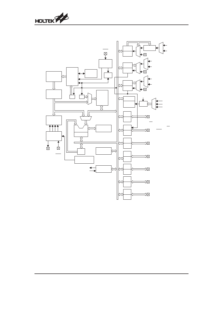
Block Diagram
HT48RU80/HT48CU80
Rev. 1.00
2
April 12, 2006
I N T 0
O S C 2
O S C 1
R E S
V D D
M U X
V S S
P r o g r a m
R O M
P r o g r a m
C o u n t e r
I n t e r r u p t
C i r c u i t
S t a c k
1 6 L e v e l s
I N T C
D a t a
M e m o r y
I n s t r u c t i o n
R e g i s t e r
M
U
X
I n s t r u c t i o n
D e c o d e r
S T A T U S
A L U
S h i f t e r
T i m i n g
G e n e r a t o r
A C C
M P
W D T S
W D T
W D T
P r e s c a l e r
M
U
X
E N / D I S
I n t e r n a l
R C O S C
P D 0 ~ P D 7
P G C
P G
P G 0 ~ P G 7
P B
P B C
P A
P A 0 ~ P A 7
P A C
P D C
P D
P C
P C C
M
U
X
M
U
X
T M R 2
f
S Y S
P E 0 ~ P E 7
P F C
P F
P F 0 ~ P F 7
P E C
P E
T M R 2 C
T M R 2
P r e s c a l e r
M
U
X
T M R 1
T M R 1 C
T M R 1
M
U
X
f
S Y S
/ 4
W D T O S C
M
U
X
T M R 0
T M R 0 C
T M R 0
M
U
X
P B 0 / B Z , P B 1 / B Z
P B 2 / I N T 1 , P B 3 / T M R 2
P B 4 ~ P B 7
E X T ( B Z , B Z )
B P
O p t i o n R O M
O T P O n l y
U A R T
T X
R X
R T C O S C
R T C O S C
R T C O S C
f
S Y S
/ 4
R T C O S C
f
S Y S
/ 4
P C 0 / T X , P C 1 / R X
P C 2 ~ P C 7
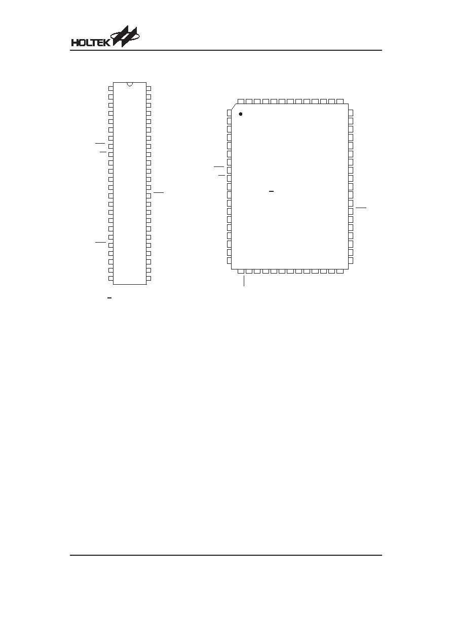
Pin Assignment
HT48RU80/HT48CU80
Rev. 1.00
3
April 12, 2006
P B 6
P B 7
P A 4
P A 5
P A 6
P A 7
P F 0
P F 1
P F 2
P F 3
O S C 2
O S C 1
V D D
R E S
T M R 1
P D 3
P D 2
P D 1
P D 0
P C 7
P C 6
P C 5
P C 4
P C 3
P B 5
P B 4
P A 3
P A 2
P A 1
P A 0
P B 3 / T M R 2
P B 2 / I N T 1
P B 1 / B Z
P B 0 / B Z
P E 3
P E 2
P E 1
P E 0
P D 7
P D 6
P D 5
P D 4
V S S
I N T 0
T M R 0
P C 0 / T X
P C 1 / R X
P C 2
P
A
6
P
A
5
P
A
4
P
B
7
P
B
6
P
B
5
P
B
4
P
G
7
P
G
6
P
G
5
P
G
4
P
A
3
P
A
2
P A 7
P F 0
P F 1
P F 2
P F 3
O S C 2
O S C 1
P F 4
P F 5
P F 6
P F 7
V D D
R E S
T M R 1
P D 3
P D 2
P D 1
P D 0
P C 7
2 0 2 1 2 2 2 3 2 4
P A 1
P A 0
P E 7
P E 6
P E 5
P E 4
P B 3 / T M R 2
P B 2 / I N T 1
P B 1 / B Z
P B 0 / B Z
P E 3
P E 2
P E 1
P E 0
P D 7
P D 6
P D 5
P D 4
V S S
P
C
6
P
C
5
P
C
4
P
C
3
P
C
2
P
C
1
/
R
X
P
C
0
/
T
X
P
G
3
P
G
2
P
G
1
P
G
0
T
M
R
0
I
N
T
0
3 2
3 1
3 0
2 9
2 8
2 7
2 6
2 5
1
2
3
4
5
6
7
8
9
1 0
1 1
1 2
1 3
1 4
1 5
1 6
1 7
1 8
1 9
5 1
5 0
4 9
4 8
4 7
4 6
4 5
4 4
4 3
4 2
4 1
4 0
3 9
3 8
3 7
3 6
3 5
3 4
3 3
6 4 6 3 6 2 6 1 6 0
5 2
5 3
5 4
5 5
5 6
5 7
5 8
5 9
H T 4 8 R U 8 0 / H T 4 8 C U 8 0
4 8 S S O P - A
H T 4 8 R U 8 0 / H T 4 8 C U 8 0
6 4 Q F P - A
4 8
4 7
4 6
4 5
4 4
4 3
4 2
4 1
4 0
3 9
3 8
3 7
3 6
3 5
3 4
3 3
3 2
3 1
3 0
2 9
2 8
2 7
2 6
2 5
1
2
3
4
5
6
7
8
9
1 0
1 1
1 2
1 3
1 4
1 5
1 6
1 7
1 8
1 9
2 0
2 1
2 2
2 3
2 4
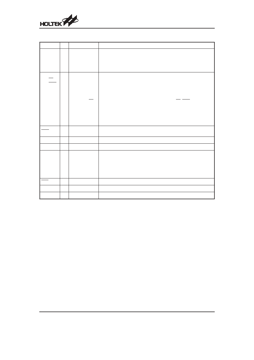
Pin Description
Pin Name
I/O
Options
Description
PA0~PA7
I/O
Pull-high
Wake-up
Schmitt Trigger
Bidirectional 8-bit input/output port. Each bit can be configured as a wake-up
input by configuration option. Software instructions determine if the pin is a
CMOS output or input. Configuration options determine if all pins on this port
have pull-high resistors and if the inputs are Schmitt trigger or non Schmitt
trigger.
PB0/BZ
PB1/BZ
PB2/INT1
PB3/TMR2
PB4~PB7
PC0/TX
PC1/RX
PC2~PC7
PD0~PD7
PE0~PE7
PF0~PF7
PG0~PG7
I/O
Pull-high
I/O or BZ/BZ
Bidirectional 8-bit input/output ports. Software instructions determine if the
pin is a CMOS output or Schmitt trigger input. A configuration option for each
port determines if all pins on the relevant port have pull-high resistors. Pins
PB0, PB1, PB2 and PB3 are pin-shared with BZ, BZ, INT1 and TMR2, re-
spectively.
Pins PC0 and PC1 are pin-shared with the UART pins TX and RX.
INT0
I
¾
External interrupt Schmitt trigger input. Edge triggered on high to low transi-
tion.
TMR0
I
¾
Schmitt trigger input for Timer/Event Counter 0
TMR1
I
¾
Schmitt trigger input for Timer/Event Counter 1
OSC1
OSC2
I
O
Crystal or RC
or Int.
RC+RTC
OSC1, OSC2 are connected to an external RC network or external Crystal
(determined by configuration option) for the internal system clock. For exter-
nal RC system clock operation, OSC2 is an output pin for 1/4 system clock.
These two pins also can be optioned as an RTC oscillator (32768Hz). In this
case, the system clock comes from an internal RC oscillator whose nominal
frequency at 5V has 4 options, 3.2MHz, 1.6MHz, 800kHz, 400kHz.
RES
I
¾
Schmitt trigger reset input. Active low.
VDD
¾
¾
Positive power supply
VSS
¾
¾
Negative power supply, ground.
Note: Each pin on PAcan be programmed through a configuration option to have a wake-up function.
Individual pins cannot be selected to have pull-high resistors. If the pull-high configuration is chosen for a partic-
ular port, then all input pins on this port will be connected to pull-high resistors.
Pins PE4~PE7 and pins PF4~PF7 only exist on the 64-pin package.
Port G only exists on the 64-pin package.
Absolute Maximum Ratings
Supply Voltage ...........................V
SS
-0.3V to V
SS
+6.0V
Storage Temperature ............................
-50°C to 125°C
Input Voltage..............................V
SS
-0.3V to V
DD
+0.3V
Operating Temperature...........................
-40°C to 85°C
Note: These are stress ratings only. Stresses exceeding the range specified under
²Absolute Maximum Ratings² may
cause substantial damage to the device. Functional operation of this device at other conditions beyond those
listed in the specification is not implied and prolonged exposure to extreme conditions may affect device reliabil-
ity.
HT48RU80/HT48CU80
Rev. 1.00
4
April 12, 2006
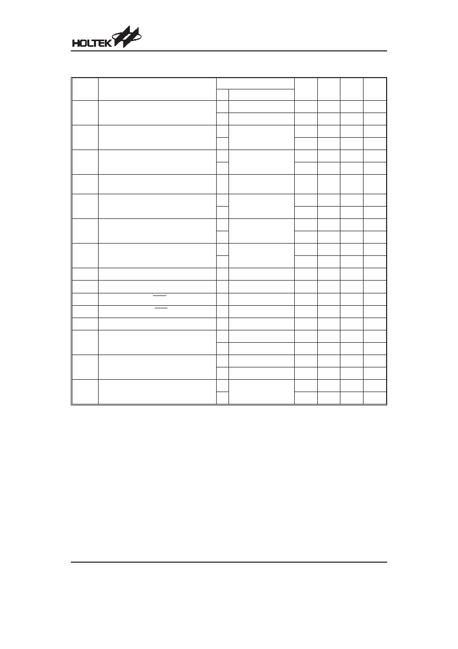
D.C. Characteristics
Ta=25
°C
Symbol
Parameter
Test Conditions
Min.
Typ.
Max.
Unit
V
DD
Conditions
V
DD
Operating Voltage
¾ f
SYS
=4MHz
2.2
¾
5.5
V
¾ f
SYS
=8MHz
3.3
¾
5.5
V
I
DD1
Operating Current (Crystal OSC)
3V
No load, f
SYS
=4MHz
¾
0.6
1.5
mA
5V
¾
2
4
mA
I
DD2
Operating Current (RC OSC)
3V
No load, f
SYS
=4MHz
¾
0.8
1.5
mA
5V
¾
2.5
4
mA
I
DD3
Operating Current
(Crystal OSC, RC OSC)
5V No load, f
SYS
=8MHz
¾
4
8
mA
I
STB1
Standby Current (WDTOSC On, RTC Off)
3V
No load, system HALT
¾
¾
5
mA
5V
¾
¾
10
mA
I
STB2
Standby Current (WDTOSC Off, RTC Off)
3V
No load, system HALT
¾
¾
1
mA
5V
¾
¾
2
mA
I
STB3
Standby Current (WDTOSC Off, RTC On)
3V
No load, system HALT
¾
¾
5
mA
5V
¾
¾
10
mA
V
IL1
Input Low Voltage for I/O Ports
¾
¾
0
¾
0.3V
DD
V
V
IH1
Input High Voltage for I/O Ports
¾
¾
0.7V
DD
¾
V
DD
V
V
IL2
Input Low Voltage (RES)
¾
¾
0
¾
0.4V
DD
V
V
IH2
Input High Voltage (RES)
¾
¾
0.9V
DD
¾
V
DD
V
V
LVR
Low Voltage Reset
¾ LVRenabled
2.7
3.0
3.3
V
I
OL
I/O Port Sink Current
3V V
OL
=0.1V
DD
4
8
¾
mA
5V V
OL
=0.1V
DD
10
20
¾
mA
I
OH
I/O Port Source Current
3V V
OH
=0.9V
DD
-2
-4
¾
mA
5V V
OH
=0.9V
DD
-5
-10
¾
mA
R
PH
Pull-high Resistance
3V
¾
20
60
100
k
W
5V
10
30
50
k
W
HT48RU80/HT48CU80
Rev. 1.00
5
April 12, 2006
Document Outline
- þÿ
- þÿ
- þÿ
- þÿ
- þÿ
- þÿ
- þÿ
- þÿ
- þÿ
- þÿ
- þÿ
- þÿ
- þÿ
- þÿ
- þÿ