 | –≠–ª–µ–∫—Ç—Ä–æ–Ω–Ω—ã–π –∫–æ–º–ø–æ–Ω–µ–Ω—Ç: HT48CXX | –°–∫–∞—á–∞—Ç—å:  PDF PDF  ZIP ZIP |

HT48CXX/HT48RXX
8-Bit Microcontroller Series
Features
∑
Operating voltage: 2.4V~5.2V
∑
Bidirectional I/O lines with a selection of 18,
22, 32 and 56 lines
∑
One interrupt input
∑
Programmable timer/event counters with
overflow interrupts and a selection of one
8-bit counter, one 8-bit and one 16-bit count-
ers, or two 16-bit counters
∑
On-chip crystal and RC oscillator
∑
Watchdog timer
∑
Program ROM with size selection of
1K
◊
14, 2K
◊
14, 4K
◊
15 and 8K
◊
16 bits
∑
Data RAM with size selection of 64
◊
8, 96
◊
8,
160
◊
8 and 224
◊
8 bits
∑
Halt function and wake-up feature to reduce
power consumption
∑
63 powerful instructions
∑
Up to 0.5
µ
s instruction cycle with 8MHz
system clock at V
DD
=5V
∑
All instructions in 1 or 2 machine cycles
∑
14-bit/15-bit/16-bit table read instructions
∑
2-level/4-level/8-level subroutine nesting
∑
Bit manipulation instructions
General Description
The HT48C10/48C30/48C50/48C70 are 8-bit
high performance RISC-like microcontrollers,
specifically designed for multiple I/O product
applications. These devices are suitable for use
in products such as remote controllers, fan/light
controllers, washing machine controllers,
scales, toys, and various subsystem controllers.
They all contain a halt feature to reduce power
consumption. The major differences between
these microcontrollers are attributed to vari-
ations in sizes of the ROM and RAM, as well as
bit number, counter number, I/O line number,
and different level subroutine nesting. Roughly
speaking, the HT48C10 is a microcontroller
with most economic features and the HT48C70
is one with the most features of the four micro-
controllers.
1
25th May '99

Selection Table
Mask version
Part No.
HT48C10
HT48C30
HT48C50
HT48C70
Operating Voltage
2.4V~5.2V
2.4V~5.2V
2.4V~5.2V
2.4V~5.2V
External Interrupt
1
1
1
1
Internal Interrupt
1
1
2
2
8-bit Timer/Event Counter
1
1
1
0
16-bit Timer/Event Counter
0
0
1
2
System Oscillator
Crystal/RC
Crystal/RC
Crystal/RC
Crystal/RC
Watchdog Timer
1
1
1
1
ROM
1K
◊
14
2K
◊
14
4K
◊
15
8K
◊
16
RAM
64
◊
8
(40H~7FH)
96
◊
8
(20H~7FH)
160
◊
8
(60H~FFH)
224
◊
8
(20H~FFH)
I/O Lines
18
22
32
56
Instructions
63
63
63
63
Stack Levels
2
2
4
8
Operating Frequency
400kHz~8MHz 400kHz~8MHz
400kHz~8MHz
400kHz~8MHz
Power Down Mode
Table Read Instructions
OTP version
Part No.
V
DD
f
SYS
I/O Pull-high
Mask version
HT48R11
3.0V~5.2V
400k~4MHz
No
HT48C10
HT48R12
3.0V~5.2V
400k~4MHz
Yes
HT48C10
HT48R31
3.0V~5.2V
400k~4MHz
No
HT48C30
HT48R32
3.0V~5.2V
400k~4MHz
Yes
HT48C30
HT48R50
3.0V~5.2V
400k~4MHz
Yes
HT48C50
HT48R51*
3.0V~5.2V
400k~4MHz
No
HT48C50
* Under development
HT48CXX/HT48RXX
2
25th May '99

Block Diagram of HT48C70
HT48CXX/HT48RXX
3
25th May '99
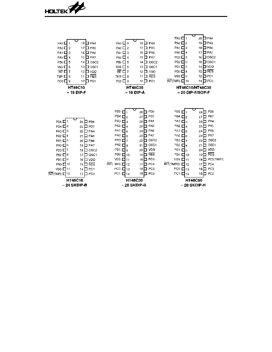
Pin Assignment
HT48CXX/HT48RXX
4
25th May '99

Note:
For the dice form, the TMR0 and TMR1 pads have to be bonded to VDD or VSS if the TMR0
and/or TMR1 pad are not used.
The (TMR0) INT indicates that the TMR0 pad should be bonded to the INT pin.
The PC5 (TMR1) indicates that the TMR1 pad should be bonded to the PC5 pin.
HT48CXX/HT48RXX
5
25th May '99

Pin Description of HT48C10
Pin Name
I/O
Mask
Option
Function
PA0~PA7
I/O
Wake-up
Pull-high
or None
Bidirectional 8-bit input/output ports
Each bit can be configured as a wake-up input by mask option.
Software instructions determine the CMOS output or schmitt
trigger input with or without pull high resistor (by mask option).
PB0~PB7
I/O
Pull-high
or None
Bidirectional 8-bit input/output ports
Software instructions determine the CMOS output or schmitt
trigger input with or without pull high resistor (by mask
option).
VSS
--
--
Negative power supply, GND
INT
I
--
External interrupt schmitt trigger input with pull high resistor
Edge trigger is activated during high to low transition.
TMR
I
--
Schmitt trigger input for timer/event counter
PC0~PC1
I/O
Pull-high
or None
Bidirectional 2-bit input/output ports
Software instructions determine the CMOS output or schmitt
trigger input with or without pull high resistor (by mask option).
RES
I
--
Schmitt trigger reset input, active low
VDD
--
--
Positive power supply
OSC1
OSC2
I
O
Crystal or
RC
OSC1 and OSC2 are connected to an RC network or a crystal
(by mask option) for the internal system clock. In the case of RC
operation, OSC2 is the output terminal for 1/4 system clock.
HT48CXX/HT48RXX
6
25th May '99

Pin Description of HT48C30
Pin Name
I/O
Mask
Option
Function
PA0~PA7
I/O
Wake-up
Pull-high
or None
Bidirectional 8-bit input/output ports
Each bit can be configured as a wake-up input by mask option.
Software instructions determine the CMOS output or schmitt
trigger input with or without a pull high resistor (by mask option).
PB0~PB7
I/O
Pull-high
or None
Bidirectional 8-bit input/output ports
Software instructions determine the CMOS output or schmitt
trigger input with or without a pull high resistor (by mask
option).
VSS
--
--
Negative power supply, GND
INT
I
--
External interrupt schmitt trigger input with a pull high
resistor. Edge triggered is activated on a high to low transition.
TMR
I
--
Schmitt trigger input for timer/event counter
PC0~PC5
I/O
Pull-high
or None
Bidirectional 6-bit input/output ports
Software instructions determine the CMOS output or schmitt
trigger input with or without a pull high resistor (by mask
option).
RES
I
--
Schmitt trigger reset input, active low
VDD
--
--
Positive power supply
OSC1
OSC2
I
O
Crystal or
RC
OSC1 and OSC2 are connected to an RC network or a crystal
(by mask option) for the internal system clock. In the case of RC
operation, OSC2 is the output terminal for 1/4 system clock.
HT48CXX/HT48RXX
7
25th May '99

Pin Description of HT48C50
Pin Name
I/O
Mask
Option
Function
PA0~PA7
I/O
Wake-up
Pull-high
or None
Bidirectional 8-bit input/output ports
Each bit can be configured as a wake-up input by mask option.
Software instructions determine the CMOS output or schmitt
trigger input with or without a pull high resistor (by mask option).
PB0~PB7
I/O
Pull-high
or None
Bidirectional 8-bit input/output ports
Software instructions determine the CMOS output or schmitt
trigger input with or without a pull high resistor (by mask
option).
VSS
--
--
Negative power supply, GND
INT
I
--
External interrupt schmitt trigger input with a pull high
resistor. Edge triggered is activated on a high to low transition.
TMR0
I
--
Schmitt trigger input for timer/event counter 0
TMR1
I
--
Schmitt trigger input for timer/event counter 1
PC0~PC7
I/O
Pull-high
or None
Bidirectional 8-bit input/output ports
Software instructions determine the CMOS output or schmitt
trigger input with or without a pull high resistor (by mask
option).
RES
I
--
Schmitt trigger reset input, active low
VDD
--
--
Positive power supply
OSC1
OSC2
I
O
Crystal or
RC
OSC1 and OSC2 are connected to an RC network or a crystal
(by mask option) for the internal system clock. In the case of RC
operation, OSC2 is the output terminal for 1/4 system clock.
PD0~PD7
I/O
Pull-high
or None
Bidirectional 8-bit Input/Output port. Software instructions
determine the CMOS output or schmitt trigger input with or
without a pull high resistor (by mask option).
HT48CXX/HT48RXX
8
25th May '99

Pin Description of HT48C70
Pin Name
I/O
Mask
Option
Function
PA0~PA7
I/O
Wake-up
Pull-high
or None
Bidirectional 8-bit input/output ports
Each bit can be configured as a wake-up input by mask option.
Software instructions determine the CMOS output or schmitt
trigger input with or without pull high resistor (by mask option).
PB0~PB7
I/O
Pull-high
or None
Bidirectional 8-bit input/output ports
Software instructions determine the CMOS output or schmitt
trigger input (pull-high depends on mask option).
VSS
--
--
Negative power supply, GND
INT
I
--
External interrupt schmitt trigger with pull high resistor
Edge trigger is activated during high to low transition.
TMR0
I
--
Schmitt trigger input for timer/event counter 0
TMR1
I
--
Schmitt trigger input for timer/event counter 1
PC0~PC7
I/O
Pull-high
or None
Bidirectional 8-bit input/output ports
Software instructions determine the CMOS output or schmitt
trigger input (pull-high depends on mask option).
RES
I
--
Schmitt trigger reset input, active low
VDD
--
--
Positive power supply
OSC1
OSC2
I
O
Crystal or
RC
OSC1 and OSC2 are connected to an RC network or a crystal
(by mask option) for the internal system clock. In the case of RC
operation, OSC2 is the output terminal for 1/4 system clock.
PD0~PD7
I/O
Pull-high
or None
Bidirectional 8-bit input/output ports
Software instructions determine the CMOS output or schmitt
trigger input (pull-high depends on mask option).
PE0~PE7
I/O
Pull-high
or None
Bidirectional 8-bit input/output ports
Software instructions determine the CMOS output or schmitt
trigger input (pull-high depends on mask option).
PF0~PF7
I/O
Pull-high
or None
Bidirectional 8-bit input/output ports
Software instructions determine the CMOS output or schmitt
trigger input (pull-high depends on mask option).
PG0~PG7
I/O
Pull-high
or None
Bidirectional 8-bit input/output ports
Software instructions determine the CMOS output or schmitt
trigger input (pull-high depends on mask option).
HT48CXX/HT48RXX
9
25th May '99

Absolute Maximum Ratings
Supply Voltage ....................... V
DD
≠0.3V to 5.5V
Storage Temperature................. ≠50
∞
C to 125
∞
C
Input Voltage .................V
SS
≠0.3V to V
DD
+0.3V
Operating Temperature .............. ≠25
∞
C to 70
∞
C
Note: These are stress ratings only. Stresses exceeding the range specified under "Absolute Maxi-
mum Ratings" may cause substantial damage to the device. Functional operation of this device
at other conditions beyond those listed in the specification is not implied and prolonged
exposure to extreme conditions may affect device reliability.
D.C. Characteristics
Ta=25
∞
C
Symbol
Parameter
Test Conditions
Min.
Typ.
Max.
Unit
V
DD
Conditions
V
DD
Operating Voltage
--
--
2.4
--
5.2
V
I
DD1
Operating Current
(HT48C10 Crystal OSC)
3V
No load
f
SYS
=4MHz
--
0.7
1.5
mA
5V
--
2
3
I
DD2
Operating Current
(HT48C10 RC OSC)
3V
No load
f
SYS
=2MHz
--
0.5
1
mA
5V
--
1
2
I
DD3
Operating Current
(HT48C30 Crystal OSC)
3V
No load
f
SYS
=4MHz
--
0.7
1.5
mA
5V
--
2
3
I
DD4
Operating Current
(HT48C30 RC OSC)
3V
No load
f
SYS
=2MHz
--
0.5
1
mA
5V
--
1
2
I
DD5
Operating Current
(HT48C50 Crystal OSC)
3V
No load
f
SYS
=4MHz
--
1
2
mA
5V
--
2.5
5
I
DD6
Operating Current
(HT48C50 RC OSC)
3V
No load
f
SYS
=2MHz
--
0.75
1.5
mA
5V
--
1.5
3
I
DD7
Operating Current
(HT48C70 Crystal OSC)
3V
No load
f
SYS
=4MHz
--
1.5
3
mA
5V
--
3.4
6
I
DD8
Operating Current
(HT48C70 RC OSC)
3V
No load
f
SYS
=2MHz
--
1
2
mA
5V
--
2.1
4
I
STB1
Standby Current
(WDT Enabled)
3V
No load
system halt
--
--
5
µ
A
5V
--
--
10
I
STB2
Standby Current
(WDT Disabled)
3V
No load
system halt
--
--
1
µ
A
5V
--
--
2
HT48CXX/HT48RXX
10
25th May '99

Symbol
Parameter
Test Conditions
Min.
Typ.
Max.
Unit
V
DD
Conditions
V
IL
Input Low Voltage for I/O
ports
3V
--
0
--
0.9
V
5V
--
0
--
1.5
V
IH
Input High Voltage for I/O
Ports
3V
--
2.1
--
3
V
5V
--
3.5
--
5
V
IL1
Input Low Voltage
(TMR, TMR0, TMR1, INT)
3V
--
0
--
0.7
V
5V
--
0
--
1.3
V
IH1
Input High Voltage
(TMR, TMR0, TMR1, INT)
3V
--
2.3
--
3
V
5V
--
3.8
--
5
V
IL2
Input Low Voltage (RES)
3V
--
--
1.5
--
V
5V
--
--
2.5
--
V
IH2
Input High Voltage (RES)
3V
--
--
2.4
--
V
5V
--
--
4.0
--
I
OL
I/O Ports Sink Current
3V
V
OL
=0.3V
1.5
4
--
mA
5V
V
OL
=0.5V
4
10
--
I
OH
I/O Ports Source Current
3V
V
OH
=2.7V
≠1
≠2
--
mA
5V
V
OH
=4.5V
≠2
≠4.5
--
R
PH
Pull-high Resistance of I/O
Ports and INT
3V
--
40
60
80
k
5V
--
10
30
50
HT48CXX/HT48RXX
11
25th May '99

A.C. Characteristics
Ta=25
∞
C
Symbol
Parameter
Test Conditions
Min.
Typ.
Max.
Unit
V
DD
Conditions
f
SYS1
System Clock (Crystal OSC)
3V
--
400
--
4000
kHz
5V
--
400
--
8000
kHz
f
SYS2
System Clock (RC OSC)
3V
--
400
--
2000
kHz
5V
--
400
--
3000
kHz
f
TIMER
Timer I/P Frequency
(TMR, TMR0, TMR1)
3V
--
0
--
4000
kHz
5V
--
0
--
4000
kHz
t
WDTOSC
Watchdog Oscillator
--
--
45
90
180
µ
s
35
65
130
t
WDT1
Watchdog Time-out
Period (RC)
--
Without WDT
prescaler
12
23
45
ms
9
17
35
t
WDT2
Watchdog Time-out Period
(System Clock)
--
Without WDT
prescaler
--
1024
--
t
SYS
t
RES
External Reset Low Pulse
Width
--
--
1
--
--
µ
s
t
SST
System Start-up Timer
Period
--
Power-up or
Wake-up from
halt
--
1024
--
t
SYS
t
INT
Interrupt Pulse Width
--
--
1
--
--
µ
s
Note: t
SYS
=1/f
SYS
HT48CXX/HT48RXX
12
25th May '99

Functional Description
The four microcontrollers of the HT48C10/
HT48C30/HT48C50/HT48C70 are constructed
using basically the same principles. Their dif-
ferences lie in variations in sizes such as ROM
and RAM as well as bit number, counter num-
ber, I/O line number, and different level subrou-
tine nesting bit number. The following is a more
detailed description of the system architectures
of the four microcontrollers. Unless specified,
the architecture stated below exists in these
four microcontrollers.
Execution flow
The system clock is derived from either a crystal
or an RC oscillator. It is internally divided into
four non-overlapping clocks. Each instruction
cycle consists of four system clock cycles.
Instruction fetching and execution are pipe-
lined in such a way that a fetch takes one in-
struction cycle while decoding and execution
takes the next instruction cycle. The pipelining
scheme causes each instruction to effectively
execute in a cycle. If an instruction changes the
program counter, two cycles are required to
complete the instruction.
Program counter ≠ PC
The program counter (PC) is of different sizes
ranging from 10 bits to 13 bits according to the
microcontroller selected (10 bits for the
HT48C10; 11 bits for the HT48C30; 12 bits for
the HT48C50; 13 bits for the HT48C70). It con-
trols a sequence in which the instructions
stored in the program ROM are executed. The
contents of the PC can specify 1024, 2048, 4096,
or 8192 addresses at maximum, according to
the microcontroller (HT48C10/HT48C30/
HT48C50/HT48C70) chosen.
After accessing a program memory word in or-
der to fetch an instruction code, the contents of
the PC is incremented by one. The PC then
points to the memory word consisting of the
next instruction code.
When executing a jump instruction, conditional
skip execution, loading a PCL register, a sub-
routine call, an initial reset, an internal inter-
rupt, an external interrupt, or returning from a
subroutine, the PC manipulates a program
transfer by loading the address corresponding
to each instruction.
The conditional skip is activated by instructions.
Once the condition is met, the next instruction,
fetched during the current instruction execution,
is discarded and a dummy cycle replaces it to get
a proper instruction; otherwise it proceeds to the
next instruction.
The lower byte of the PC (PCL) is a readable
and writeable register (06H). Moving data into
the PCL performs a short jump. The destination
is within 256 locations.
For a control transfer to take place, an addi-
tional dummy cycle is required.
Execution flow
HT48CXX/HT48RXX
13
25th May '99

Mode
Contents of Program Counter (m bits)
Initial reset
0000H
External interrupt
0004H
Timer/event counter 0 overflow
0008H
Timer/event counter 1 overflow
000CH
Skip
PC+2
Loading PCL
Low byte replaced by instruction code
Jump, call branch
Instruction code
Return from subroutine
Stack register
Notes: m=10 for the HT48C10
m=11 for the HT48C30
m=12 for the HT48C50
m=13 for the HT48C70
Program memory ≠ ROM
The program memory (ROM) is used to store the
program instructions that are to be executed. It
contains data, table, and interrupt entries, and
is organized into 1024
◊
14 bits, 2048
◊
14 bits,
4096
◊
15 bits, or 8192
◊
16 bits according to the mi-
crocontroller (HT48C10/ HT48C30/HT48C50/
HT48C70) selected. These bits are all addressed by the
PC and table pointer.
Certain locations in the ROM stated below are
reserved for special usage in the four microcon-
trollers except location 00CH which is used for
the HT48C50/HT48C70 exclusively.
∑
Location 000H
Location 000H is reserved for program in-
itialization. After chip reset, the program al-
ways begins execution at this area.
∑
Location 004H
Location 004H is reserved for external inter-
rupt service program. If the INT input pin is
activated, the interrupt is enabled, and the
stack is not full, the program begins execution
at location 004H.
∑
Location 008H
Location 008H is reserved for the timer/event
counter interrupt service program of the
HT48C10/HT48C30 and for the timer/event
counter 0 interrupt service program of the
HT48C50/HT48C70. If the timer interrupt re-
sults from a timer/event counter overflow of
the HT48C10/HT48C30 or a timer/event
counter 0 overflow of the HT48C50/HT48C70,
and the interrupt is enabled, and the stack is
not full, the program begins execution at loca-
tion 008H.
Program memory
HT48CXX/HT48RXX
14
25th May '99

∑
Location 00CH
Location 00CH is reserved for the timer/ event
counter 1 interrupt service program of the
HT48C50/HT48C70 only. If the timer inter-
rupt results from a timer/event counter 1
overflow, the interrupt is enabled, and the
stack is not full, the program begins execution
at location 00CH.
∑
Table location
Any location in the ROM can be used as a
look≠up table. The instructions TABRDC [m]
(the current page, 1 page=256 words) and
TABRDL [m] (the last page) transfer the con-
tents of the lower-order byte to the specified
data memory, and the higher-order byte to
TBLH (08H). Only the destination of the
lower-order byte in the table is well-defined,
and the higher-order byte of the table word is
transferred to the Table Higher-order byte
register (TBLH). The TBLH is read only. The
Table Pointer (TBLP), on the other hand, is a
read/write register (07H) used to indicate the
table location. Before accessing the table, the
location should be placed in the TBLP. The
TBLH is read only and cannot be restored. If
the main routine and the ISR (Interrupt Serv-
ice Routine) both employ the table read in-
struction, the contents of the TBLH in the
main routine is likely to be changed by the
table read instruction used in the ISR. Errors
will then occur. Hence, simultaneously using
the table read instruction in the main routine
and the ISR should be avoided. Nonetheless,
if the application of the table read instruction
to both the main routine and the ISR cannot
be avoided, interrupts should be disabled
prior to the table read instruction, and they
should not be enabled until the TBLH is
backed-up. All the table related instructions
require 2 cycles to complete an operation.
These areas may function as a normal pro-
gram memory depending upon the user's re-
quirements.
Stack register ≠ STACK
The stack register is a special memory port used
to save the contents of the PC. The stack can be
organized into 2, 4, or 8 levels according to the
microcontroller selected (2 levels for the
HT48C10/HT48C30, 4 levels for the HT48C50,
8 levels for the HT48C70). The register is nei-
ther part of the data nor part of the program,
and is neither readable nor writeable. Any acti-
vated level is indexed by a stack pointer (SP)
and is neither readable nor writeable. At a sub-
routine call or interrupt acknowledgment, the
contents of the PC is pushed onto the stack. At
the end of a subroutine or an interrupt routine,
signaled by a return instruction (RET or RETI),
the contents of the PC is restored to its previous
value from the stack. After chip reset, the SP
will point to the top of the stack.
If the stack is full and a non-masked interrupt
takes place, the interrupt request flag is recorded
but the acknowledgment is still inhibited. After
the stack pointer is decremented (by RET or
RETI), the interrupt will be serviced. This feature
prevents the occurrence of stack overflow, allow-
Instruction(s)
Table Location
*m~*8
7
6
5
4
3
2
1
0
TABRDC [m]
Pm~P8
@7
@6
@5
@4
@3
@2
@1
@0
TABRDL [m]
1~1
@7
@6
@5
@4
@3
@2
@1
@0
Table location
Notes:
m~
0: Bits of table location
@7~@0: Bits of table pointer
Pm~P8: Bits of current
Program Counter
m=9 for the HT48C10
m=10 for the HT48C30
m=11 for the HT48C50
m=12 for the HT48C70
HT48CXX/HT48RXX
15
25th May '99
ing the programmer to use the structure easily.
Likewise, if the stack is full and a CALL is
subsequently executed, a stack overflow will
occur and the first entry will be lost (only the
most recent four return addresses will be
stored).
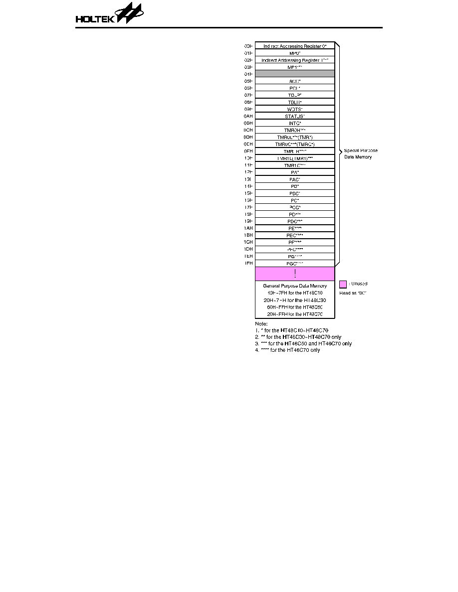
Data memory ≠ RAM
The data memory (RAM) is composed of bits
ranging from 81
◊
8, 113
◊
8, 184
◊
8, or 255
◊
8, de-
pending on the microcontroller chosen
(HT48C10/ HT48C30/HT48C50/HT48C70). It is
divided into two functional groups, i.e., special
function registers and general purpose data
memory (of 64
◊
8, 96
◊
8, 160
◊
8, or 224
◊
8 bits,
depending on the microcontroller selected
(HT48C10/ HT48C30/HT48C50/HT48C70).
Most components of the two functional groups
are readable/writable, but some are read-only.
Of the two functional groups, the special func-
tion registers of the four microcontrollers con-
sist of a program counter lower-order byte
register (PCL;06H), an accumulator (ACC;
05H), a table pointer (TBLP;07H), a table
higher-order byte register (TBLH;08H), a
status register (STATUS;0AH), an interrupt
control register (INTC;0BH), a watchdog timer
option setting register (WDTS;09H), an indirect
addressing register (00H), a memory pointer
register (MP;01H), a timer/event counter
(TMR;0DH), a timer/event counter control reg-
ister (TMRC;0EH), I/O re gisters
(PA;12H,PB;14H, PC;16H), and I/O control reg-
isters (PAC;13H,PBC;15H,PCC;17H). But of
the HT48C50/HT48C70, the following compo-
nents are further divided into two or several
sub-components. First, the indirect addressing
register is divided into two registers involving
indirect addressing register 0 (00H) and indi-
rect addressing register 1 (02H). Second, the
memory pointer register is also comprised by
two registers involving memory pointer register
0 (MP0;01H) and memory pointer register 1
(MP1;03H). Third, the timer/event counter reg-
ister is organized by two registers according to
different orders of byte, namely timer/event
higher-order byte register and timer/event
lower-order byte register, both of which are fur-
ther divided into timer/event counter 0 higher-
order byte register (TMR0H; 0CH), timer/ event
counter 1 higher-order byte register
(TMR1H;0FH), timer/event counter 0 lower-or-
der byte re gister (TMR0L;0DH), and
timer/event counter 1 lower-order byte register
(TMR1L;10H). Fourth, the timer/event counter
control register is divided into two registers
involving timer/event counter 0 control register
RAM mapping
HT48CXX/HT48RXX
16
25th May '99

(TMR0C;0EH) and timer/event counter 1 con-
trol register (TMR1C;11H). Fifth, the entire
number of I/O registers is expanded from 3 to 6
(PA;12H,PB;14H,PC;16H,PD;18H,PE;1AH,
PF;1CH,PG; 1EH). Finally, the number of I/O
control registers is also doubled (PAC;13H,
P B C ; 1 5 H , P C C ; 1 7 H , P D C ; 1 9 H , P E C ; 1 B H ,
PFC;1DH,PGC;1FH). The remaining space be-
fore the 20H of the four microcontrollers are all
reserved for future expansion usage. Reading
these remaining locations will return the result
to 00H. The general purpose data memory, ad-
dressed from 40H~7FH of the HT48C10,
20H~7FH of the HT48C30, 60H~FFH of the
HT48C50, or 20H~FFH of the HT48C70 accord-
ing to the microcontroller selected, is used for
data and control information under instruction
commands.
All the RAM areas can directly execute arithme-
tic, logic, increment, decrement, and rotate op-
erations. Except some dedicated bits, each bit in
the RAM can be set and reset by the SET [m].i
and CLR [m].i instructions, respectively. These
RAM areas are indirectly accessible through the
memory pointer register(s) MP (01H) of the
HT48C10/HT48C30 or MP0 (01H) and MP1
(03H) of the HT48C50/HT48C70.
Indirect addressing register
Of the four microcontrollers, the HT48C10/
HT48C30 make use of location 00H whereas the
HT48C50/HT48C70 of locations 00H and 02H
as indirect addressing registers that are not
physically implemented. Any read/write opera-
tion of [00H] or of [00H] and [02H] accesses the
RAM pointed to by MP (01H) or by MP0 (01H)
and MP1 (03H) respectively according to the
microcontroller chosen. Reading location 00H or
02H indirectly will return the result 00H. Writ-
ing it indirectly will, result to no operation.
The function of data movement between two
indirect addressing registers is not supported.
The memory pointer register MP of the
HT48C10/HT48C30 or MP0 and MP1 of the
HT48C50/HT48C70 are of 7 bits or 8 bits wide
respectively, and can be used to access the RAM
by combining the corresponding indirect ad-
dressing registers. The bit 7 of MP
(HT48C10/HT48C30) is undefined and reading
will return the result "1". Any writing operation to
MP will only transfer the lower 7-bit data to MP.
Accumulator ACC
The accumulator (ACC) relates to the ALU op-
erations. It is also mapped to location 05H of the
RAM and is capable of operating with immedi-
ate data. The data movement between two data
memories will pass through the ACC.
Arithmetic and logic unit ≠ ALU
This circuit performs 8-bit arithmetic and logic
operations. It provides the following functions:
∑
Arithmetic operations (ADD, ADC, SUB,
SBC, DAA)
∑
Logic operations (AND, OR, XOR, CPL)
∑
Rotation (RL, RR, RLC, RRC)
∑
Increment and Decrement (INC, DEC)
∑
Branch decision (SZ, SNZ, SIZ, SDZ, etc.)
The ALU saves the results of the data operation
and change the status register as well.
Status register ≠ STATUS
The status register (0AH) is of 8 bits wide and
consists of a zero flag (Z), a carry flag (C), an
auxiliary carry flag (AC), an overflow flag (OV),
a power down flag (PD), and a watchdog time-
out flag (TO). The register also records the status
information and controls the operation sequence.
Except the TO and PD flags, bits in the status
register can all be altered by instructions, simi-
lar to the case with other registers. Any data
written into the status register will not change
the TO or PD flags. But the operations related
to the status register may lead to different re-
sults from those intended. The TO and PD flags
can be changed by system power up, Watchdog
Timer overflow, executing the HALT instruc-
tion, or clearing the Watchdog Timer. The Z, OV,
AC, and C flags all reflect the status of the
latest operations.
HT48CXX/HT48RXX
17
25th May '99

Labels
Bits
Function
C
0
C is set if the operation results in a carry during an addition operation or if a
borrow does not take place during a subtraction operation; otherwise C is
cleared. Also it is affected by a rotate through carry instruction.
AC
1
AC is set if the operation results in a carry out of the low nibbles in addition or
no borrow from the high nibble into the low nibble in subtraction; otherwise AC
is cleared.
Z
2
Z is set if the result of an arithmetic or logic operation is zero; otherwise Z is
cleared.
OV
3
OV is set if the operation results in a carry into the highest-order bit but not a
carry out of the highest-order bit, or vice versa; otherwise OV is cleared.
PD
4
PD is cleared by either a system power-up or executing the CLR WDT
instruction. PD is set by executing the HALT instruction.
TO
5
TO is cleared by a system power-up or executing the CLR WDT or HALT
instruction. TO is set by a WDT time-out.
--
6
Undefined, read as 0
--
7
Undefined, read as 0
Status register
On entering the interrupt sequence or execut-
ing the subroutine call, the status register will
not be automatically pushed onto the stack . If
the contents of the status is important and the
subroutine can corrupt the status register, the
programmer should take precautions to save it
properly.
Interrupt
The four microcontrollers all provide an exter-
nal interrupt and internal timer/event counter
interrupts. The interrupt control register
(INTC;0BH) contains interrupt control bits for
setting the enable/disable mode and the interrupt
request flags.
Once an interrupt subroutine is serviced, the
remaining interrupts will all be blocked (by
clearing the EMI bit). This scheme may prevent
any further interrupt nesting. Other interrupt
requests may happen during this interval but
only the interrupt request flag will be recorded.
If a certain interrupt requires servicing within
the service routine, the programmer may set the
EMI bit and the corresponding bit of INTC so as
to allow interrupt nesting. If the stack is full, the
interrupt request will not be acknowledged, even
if the related interrupt is enabled, until the SP
is decremented. If immediate servicing is de-
sired, the stack should be prevented from be-
coming full.
All these interrupts have a wake-up capability.
As an interrupt is serviced, a control transfer
occurs by pushing the PC onto the stack and
then by branching it to subroutines at the speci-
fied location(s) in the ROM. Only the contents of
the PC can be pushed onto the stack. If the
contents of the register and of the status regis-
ter (STATUS) are altered by the interrupt serv-
ice program which corrupts the desired control
sequence, the programmer should save these
contents first.
The external interrupt is triggered by a high to
low transition of the INT, and the related inter-
rupt request flag (EIF; bit 4 of INTC) is then set.
When the interrupt is enabled, the stack is not
full, and the external interrupt is active, a sub-
routine call to location 04H will occur. The inter-
rupt request flag (EIF) and EMI bits will also be
cleared to disable other interrupts.
Of the four microcontrollers, the internal
timer/event counter interrupt of the HT48C10/
HT48C30 is initialized by setting the timer/
HT48CXX/HT48RXX
18
25th May '99
Register
Bit No.
Label
Function
INTC
(0BH)
0
EMI
Control the master (global) interrupt
(1= enabled; 0= disabled)
1
EEI
Control the external interrupt
(1= enabled; 0= disabled)
2
ET0I
Control the timer/event counter 0 interrupt
(1= enabled; 0= disabled)
3
ET1I
Control the timer/event counter 1 interrupt (for the
HT48C50/HT48C70 only) (1= enabled; 0= disabled)
4
EIF
External interrupt request flag
(1= active; 0= inactive)
5
T0F
Internal timer/event counter 0 request flag
(1= active; 0= inactive)
6
T1F
Internal timer/event counter 1 request flag (for the
HT48C50/HT48C70 only) (1= active; 0= inactive)
7
--
Unused bit, read as "0"
INTC register
event counter interrupt request flag (TF; bit 5 of
INTC), that is caused by a timer overflow. When
the interrupt is enabled, and the stack is not
full, and the TF bit is set, a subroutine call to
location 08H will occur. The related interrupt
request flag (TF) will be reset and the EMI bit
will be cleared to disable further interrupts.
The internal timer/event counter of the
HT48C50/HT48C70, is composed of two inter-
rupts, namely internal timer/event counter 0
interrupt and timer/event counter 1 interrupt.
The internal timer/event counter 0 interrupt is
initialized by setting the timer/event counter 0
interrupt request flag (T0F; bit 5 of INTC)
which is caused by a timer/event counter 0 over-
flow. After the interrupt is enabled, the stack is
not full, and the T0F bit is set, a subroutine call
to location 08H will occur. The related interrupt
request flag (T0F) will be reset and the EMI bit
be cleared to disable further interrupts. On the
other hand, the timer/event counter 1 interrupt
is operated in the same manner as the timer/
event counter 0. The related interrupt control
bits ET1I and T1F of the timer/event counter 1
are bit 3 and bit 6 of the INTC, respectively.
During the execution of an interrupt subroutine
of the four microcontrollers, other interrupt ac-
knowledgments are all held until the RETI in-
struction is executed or the EMI bit and the
related interrupt control bit are both set to 1
(when the stack is not full). To return from the
interrupt subroutine, the RET or RETI instruc-
tion may be invoked. The RETI will set the EMI
bit in order to enable an interrupt service
whereas the RET will not.
Interrupts that occur in an interval between the
rising edges of two consecutive T2 pulses are
serviced on the latter of the two T2 pulses if the
corresponding interrupts are enabled. In case of
simultaneous requests, the following table
shows the priority that is applied. These can be
masked by resetting the EMI bit.
No. Interrupt Source Priority Vector
a
External interrupt
1
04H
b
Timer/event
counter 0 overflow
2
08H
*c
Timer/event
counter 1 overflow
3
0CH
* Note: c applies only to the HT48C50/ HT48C70
HT48CXX/HT48RXX
19
25th May '99

The timer/event counter interrupt request flag
(TF), external interrupt request flag (EIF), en-
able timer/event counter bit (ETI), enable exter-
nal interrupt bit (EEI), and enable master
interrupt bit (EMI) constitute an interrupt con-
trol register (INTC) of the HT48C10/HT48C30
which is located at 0BH in the RAM. On the
other hand, the timer/event counter 0/1 inter-
rupt request flag (T0F/T1F), external interrupt
request flag (EIF), enable timer/event counter
0/1 bit (ET0I/ET1I), enable external interrupt
bit (EEI), and enable master interrupt bit (EMI)
make up the interrupt control register (INTC) of
the HT48C50/HT48C70 which is located at 0BH
in the RAM. EMI, EEI, and ETI, of the
HT48C10/HT48C30 or EMI, EEI, ET0I, and
ET1I of the HT48C50/HT48C70 are all used to
control the enable/disable status of interrupts.
These bits prevent the requested interrupt from
being serviced. Once the interrupt request flags
(TF, EIF of the HT48C10/HT48C30 or T0F, T1F,
EIF of the HT48C50/HT48C70) are set, they
will remain in the INTC register until the inter-
rupts are all serviced or cleared by a software
instruction.
It is suggested that a program should not em-
ploy the "CALL subroutine" within the inter-
rupt subroutine, since its operation within the
interrupt subroutine may damage the original
control sequence, and interrupts often occur in
an unpredictable manner or it may need imme-
diate servicing for certain applications. Given
this, if only one stack is left and enabling the
interrupt is not well controlled, the original con-
trol sequence may be ruined as a result of operating
the CALL subroutine in the interrupt subroutine.
Oscillator configuration
There are 2 oscillator circuits available, namely
RC oscillator and crystal oscillator, decided by
mask options. Both are designed for system
clocks. No matter what type of oscillator is cho-
sen, the signal supports the system clock. The
HALT mode stops the system oscillator and ig-
nores any external signals so as to conserve
power.
Of the two oscillator types, if an RC oscillator is
used, an external resistor between OSC1 and
VDD is required and its resistance ranges from
51k
to 1M
. The system clock, divided by 4, is
available on OSC2 (NMOS open drain output),
which can be used to synchronize external logic.
The RC oscillator provides the most cost effec-
tive solution. However, the frequency of the os-
cillation may vary with VDD, temperature and
the chip itself due to process variations. It is,
therefore, not suitable for timing sensitive op-
erations where accurate oscillator frequency is
desired. On the other hand, if the crystal oscil-
lator is used, a crystal across OSC1 and OSC2
is needed to provide the feedback and phase
shift required for the crystal oscillator. No other
external components are required. Instead of a
crystal, the resonator can also be connected be-
tween OSC1 and OSC2 to derive a frequency
reference, but two external capacitors in OSC1
and OSC2 are required.
The WDT oscillator is a free running on-chip RC
oscillator, and no external components are re-
quired. Even if the system enters the power
down mode, the system clock is stopped but the
WDT oscillator still works with a period of ap-
proximately 78
µ
s. The WDT oscillator can be
disabled by mask option to conserve power.
Watchdog timer ≠ WDT
The clock source of the WDT is implemented by
a dedicated RC oscillator (WDT oscillator) or an
instruction clock (system clock divided by 4),
decided by mask options. The WDT is designed
to prevent a software malfunction or sequence
from jumping to an unknown location with un-
predictable results. The WDT can be disabled
by mask option. If the WDT is disabled, all the
executions related to the WDT may lead to no
operation.
System oscillator
HT48CXX/HT48RXX
20
25th May '99

Watchdog timer
If the internal WDT oscillator (RC oscillator
with a period of 78
µ
s normally) is selected, it is
first divided by 256 (8 stages) to derive a nomi-
nal time-out period of about 20ms. This time-
out period may vary with temperature, VDD,
and process variations. By invoking the WDT
prescaler, longer time-out periods can be real-
ized. Writing data to WS2, WS1, and WS0 (bit
2,1,0 of the WDTS) can lead to different time-
out periods. If the values of WS2, WS1, and WS0
all equal to 1, the division ratio is up to 1:128,
and the maximum time-out period is 2.6 sec-
onds.
But if the WDT oscillator is disabled, the WDT
clock may still come from the instruction clock
and operate in the same manner except that in
the HALT state the WDT may stop counting
and lose its protecting purpose. In this situation
the logic can be restarted by external logic. The
high nibble and bit 3 of the WDTS are reserved
for user defined flags, and the programmer may
use these flags to indicate some specified status.
WS2
WS1
WS0
Division Ratio
0
0
0
1:1
0
0
1
1:2
0
1
0
1:4
0
1
1
1:8
1
0
0
1:16
1
0
1
1:32
1
1
0
1:64
1
1
1
1:128
WDTS Register
If the device operates in a noisy environment,
using the on-chip RC oscillator (WDT OSC) is
strongly recommended, since the HALT will ter-
minate the system clock.
The overflow of WDT under normal operation
can initialize "chip reset" and set the status bit
TO. But in the HALT mode, the overflow will
initialize a "warm reset", and only the PC and
SP are reset to zero. To clear the contents of
WDT (the WDT prescaler included), three
methods can be adopted, i.e., external reset (a
low level to RES), software instruction(s), and a
HALT instruction. The software instruction(s)
consists of CLR WDT and the other set -- CLR
WDT1 and CLR WDT2. Of these two types of
instructions, only one type can be active de-
pending on mask option -- "CLR WDT times
selection option". If the "CLR WDT" is chosen
(i.e., CLRWDT times equal one), any execution
of the CLR WDT instruction will clear the WDT.
In the case that the "CLR WDT1" and "CLR
WDT2" are chosen (i.e., CLRWDT times equal
two), these two instructions should be executed
to clear the WDT; otherwise, the WDT may
reset the chip due to time-out.
Power down operation ≠ HALT
The HALT mode is initialized by the HALT
instruction and results in the following.
∑
The system oscillator turns off but the WDT
oscillator keeps running (if the WDT oscillator
is selected).
∑
The contents of the on≠chip RAM and regis-
ters remain unchanged.
∑
The WDT and WDT prescaler are cleared and
recount (if the WDT clock comes from the
WDT oscillator).
∑
All I/O ports maintain their original status.
∑
The PD flag is set and the TO flag is cleared.
The system can quit the HALT mode by exter-
HT48CXX/HT48RXX
21
25th May '99

nal reset, interrupt, external falling edge signal
on port A, or a WDT overflow. An external reset
may cause device initialization, and the WDT
overflow performs a "warm reset". Examining the
TO and PD flags, the reason for chip reset is
determined. The PD flag is cleared by system
power-up or executing the CLR WDT instruction,
and is set by executing the HALT instruction. The
TO flag is set if the WDT time-out occurs, and
causes a wake-up that resets the PC and SP only.
The others maintain their original status.
The port A wake-up and interrupt methods can
be considered as a continuation of normal exe-
cution. Each bit in port A can be independently
selected to wake up the device by mask option.
Awakening from an I/O port stimulus, the pro-
gram will resume execution of the next instruc-
tion. On the other hand, awakening from an
interrupt, two sequences may happen. If the
related interrupt(s) is disabled or the inter-
rupt(s) is enabled but the stack is full, the pro-
gram will resume execution at the next
instruction. But if the interrupt is enabled and
the stack is not full, the regular interrupt re-
sponse takes place.
When wake-up event(s) occurs, it takes 1024
t
SYS
(system clock period) to resume normal
operation. That is to say, a dummy period is
inserted after the wake-up. If the wake-up re-
sults from an interrupt acknowledgment, the
actual interrupt subroutine execution will be
delayed by more than one cycle. But if the wake-
up results in the next instruction execution, the
instruction will execute immediately after the
dummy period is finished. If an interrupt re-
quest flag is set to "1" before entering the HALT
mode, the make-up function of the related inter-
rupt will be disabled.
To minimize power consumption, all the I/O
pins should be carefully managed before enter-
ing the HALT status.
Reset
There are three ways in which reset may occur:
∑
RES is reset during normal operation
∑
RES is reset during HALT
∑
WDT timeout is reset during normal operation
WDT time-out during the HALT is different
from other chip reset conditions, for it can per-
form a "warm reset" that resets only PC and SP
and leaves the other circuits at their original
state. Some registers remain unchanged during
any other reset conditions. Most of the registers
are reset to the "initial condition" when the
reset conditions are met. By examining the PD
flag and TO flag, the program distinguishes
between different "chip resets".
TO
PD
RESET Conditions
0
0
RES reset during power-up
u
u
RES reset during normal
operation
0
1
RES wake-up HALT
Reset timing chart
Reset circuit
Reset configuration
HT48CXX/HT48RXX
22
25th May '99

TO
PD
RESET Conditions
1
u
WDT time-out during normal
operation
1
1
WDT wake-up HALT
Note: "u" means "unchanged"
To guarantee that the system oscillator is
started and stabilized, the SST (System Start-
up Timer) provides an extra-delay. The extra-
delay delays 1024 system clock pulses when the
system powers up or awakes from the HALT
state.
When the system power-up occurs, the SST de-
lay is added during the reset period. But when
the reset comes from the RES pin, the SST delay
is disabled. Any wake-up from HALT will enable
the SST delay.
The status of the chip reset of the functional
units are as shown.
PC
000H
Interrupt
Disabled
Prescaler
Cleared
WDT
Cleared
After a master reset,
WDT begins counting.
Timer/event
counter (0/1)
Off
Input/output ports
Input mode
SP
Point to the top of the
stack
Timer/event counter
There are two timer/event counters imple-
mented in the four microcontrollers. Of the four
microcontrollers, the timer/event counter of the
HT48C10/HT48C30 contains an 8-bit program-
mable count-up counter. On the other hand, the
timer/event counter of the HT48C50/HT48C70
composes of two counters, namely timer/event
counter 0 and timer/event counter 1. The
timer/event counter 0 contains a 16-bit pro-
grammable counter, and the timer/event
counter 1 contains an 8-bit programmable
count-up counter of the HT48C50. The
timer/event counters 0 and 1 of the HT48C70
both contain a 16-bit programmable count-up
counter. The source of the clock of the four mi-
crocontrollers may come from an external
source or the system clock divided by 4. If the
internal instruction clock is applied, only one
reference time-base is available. The external
clock input, on the other hand, allows the user
to count external events, measure time inter-
vals or pulse width, or generate an accurate
time base.
Of the HT48C10/HT48C30, there are two regis-
ters related to the timer/event counter, i.e.,
TMR ([0DH]) and TMRC ([0EH]). There are two
physical registers mapped to the TMR location.
Writing TMR puts the starting value in the
timer/event counter preload register while
reading TMR gets the contents of the timer/
event counter. The TMRC, on the other hand, is
a timer/event counter control register.
Timer/event counter 0/1
HT48CXX/HT48RXX
23
25th May '99
The states of the special function registers are summarized in the following table:
Register
Reset
(power on)
WDT time-out
(normal
operation)
RES reset
(normal
operation)
RES reset
(HALT)
WDT
time-out*
(HALT)
TMR1H
xxxx xxxx
uuuu uuuu
uuuu uuuu
uuuu uuuu
uuuu uuuu
TMR1L
xxxx xxxx
uuuu uuuu
uuuu uuuu
uuuu uuuu
uuuu uuuu
TMR1C
00-0 1---
00-0 1---
00-0 1---
00-0 1---
uu-u u---
TMR0H
xxxx xxxx
uuuu uuuu
uuuu uuuu
uuuu uuuu
uuuu uuuu
TMR0L
xxxx xxxx
uuuu uuuu
uuuu uuuu
uuuu uuuu
uuuu uuuu
TMR0C
00-0 1---
00-0 1---
00-0 1---
00-0 1---
uu-u u---
PC
000H
000H
000H
000H
000H
MP0
xxxx xxxx
uuuu uuuu
uuuu uuuu
uuuu uuuu
uuuu uuuu
MP1
xxxx xxxx
uuuu uuuu
uuuu uuuu
uuuu uuuu
uuuu uuuu
ACC
xxxx xxxx
uuuu uuuu
uuuu uuuu
uuuu uuuu
uuuu uuuu
TBLP
xxxx xxxx
uuuu uuuu
uuuu uuuu
uuuu uuuu
uuuu uuuu
TBLH
xxxx xxxx
uuuu uuuu
uuuu uuuu
uuuu uuuu
uuuu uuuu
STATUS
--00 xxxx
--1u uuuu
--uu uuuu
--01 uuuu
--11 uuuu
INTC
-000 0000
-000 0000
-000 0000
-000 0000
-uuu uuuu
WDTS
0000 0111
0000 0111
0000 0111
0000 0111
uuuu uuuu
PA
1111 1111
1111 1111
1111 1111
1111 1111
uuuu uuuu
PAC
1111 1111
1111 1111
1111 1111
1111 1111
uuuu uuuu
PB
1111 1111
1111 1111
1111 1111
1111 1111
uuuu uuuu
PBC
1111 1111
1111 1111
1111 1111
1111 1111
uuuu uuuu
PC
1111 1111
1111 1111
1111 1111
1111 1111
uuuu uuuu
PCC
1111 1111
1111 1111
1111 1111
1111 1111
uuuu uuuu
PD
1111 1111
1111 1111
1111 1111
1111 1111
uuuu uuuu
PDC
1111 1111
1111 1111
1111 1111
1111 1111
uuuu uuuu
PE
1111 1111
1111 1111
1111 1111
1111 1111
uuuu uuuu
PEC
1111 1111
1111 1111
1111 1111
1111 1111
uuuu uuuu
PF
1111 1111
1111 1111
1111 1111
1111 1111
uuuu uuuu
PFC
1111 1111
1111 1111
1111 1111
1111 1111
uuuu uuuu
PG
1111 1111
1111 1111
1111 1111
1111 1111
uuuu uuuu
PGC
1111 1111
1111 1111
1111 1111
1111 1111
uuuu uuuu
Note:
"
" means "warm reset"
"u" means "unchanged"
"x" means "unknown"
"≠" means "undefined"
The bits of the special function registers are denoted as "≠" if they are not defined
in the microcontrollers.
HT48CXX/HT48RXX
24
25th May '99

Of the HT48C50/HT48C70, the timer/event
counter is comprised by two counters, i.e.,
timer/event counter 0 and timer/event counter
1. There are three registers related to the
timer/event counter 0, namely TMR0H (0CH),
TMR0L (0DH), and TMR0C (0EH). Writing
TMR0L only writes the data into a low byte
buffer, but writing TMR0H writes the data
along with the contents of the low byte buffer
into the timer/event counter 0 preload register
(16-bit). The timer/event counter 0 preload reg-
ister is changed by writing the TMR0H opera-
tions, and writing TMR0L keeps the timer/
event counter 0 preload register unaltered.
Also, reading the TMR0H latches the TMR0L
into the low byte buffer in order to avoid the
false timing problem. Then, reading the TMR0L
will return the contents of the low byte buffer.
In other words, the low byte of the timer/event
counter 0 cannot be read directly. Instead it has
to read the TMR0H first in order to make the
low byte contents of the timer/event counter 0
latched into the buffer. On the other hand, there
are also thre e registe rs relate d to the
timer/event counter 1, namely TMR1H (0FH),
TMR1L (10H), and TMR1C (11H). The timer/
event counter 1 operates in the same manner as
the timer/event counter 0.
The TMR0C is a timer/event counter 0 control
register defining the timer/event counter 0 op-
tions. The timer/event counter 1 has the same
options as the timer/event counter 0 and is de-
fined by TMR1C.
The timer/event counter control registers of the
four microcontrollers are all used to define the
operation mode, counting enable or disable, and
active edge.
The TM0 and TM1 bits define the operation
mode. The event count mode is used to count
external events, which means that the clock
source comes from an external pin TMR of the
HT48C10/HT48C30 or TMR0/TMR1 of the
HT48C50/HT48C70. The timer mode functions
as a normal timer with the clock source coming
from the instruction clock. The pulse width
measurement mode can be used to count the
high or low level duration of the external signal
TMR of the HT48C10/HT48C30 or TMR0/TMR
1 of the HT48C50/HT48C70. The counting is
based on the instruction clock.
In the event count or timer mode, once the
timer/event counter starts counting, it will count
from the current contents in the timer/event
counter to FFH of the HT48C10/HT48C30/
HT48C50 (TMR1) or to FFFFH of the HT48C50
(TMR0)/HT48C70. If an overflow occurs, the
counter is reloaded from the timer/ event counter
preload register and generates the corresponding
interrupt request flag TF (bit 5 of INTC) of the
HT48C10/HT48C30 or T0F/T1F (bit 5/6 of INTC)
of the HT48C50/ HT48C70 at the same time.
Label
Bits
Function
--
0~2
Unused bits, read as "0"
TE
3
To define TMR0/TMR1 active edge of the timer/event counter
(0= active on low to high; 1= active on high to low)
TON
4
To enable/disable timer counting
(0= disabled; 1= enabled)
--
5
Unused bits, read as "0"
TM0
TM1
6
7
To define the operating mode
01= Event count mode (external clock)
10= Timer mode (internal clock)
11= Pulse width measurement mode
00= Unused
TMR0C/TMR1C register
HT48CXX/HT48RXX
25
25th May '99

In the pulse width measurement mode with the
values of the TON and TE bits equal to one, if the
TMR0/ TMR1 has received a transient from low
to high (or high to low; if the TE bit is 0) it will
start counting until the TMR of the
HT48C10/HT48C30 or TMR0/TMR1 of the
HT48C50/ HT48C70 returns to the original level
and resets the TON. The measured result re-
mains in the timer/event counter even if the
activated transient happens again. In other
words, only one cycle measurement can be done.
Until setting the TON, the cycle measurement
will re-function as long as it receives further
transient pulse. In this operation mode, the
timer/event counter starts counting according
not to the logic level but to the transient edges.
In the case of counter overflows, the counter is
reloaded from the timer/event counter preload
register and issues an interrupt request just like
the other two modes.
To enable the counting operation, the timer ON
bit (TON; bit 4 of TMRC of the HT48C10/
HT48C30 or bit 4 of TMR0C/TMR1C of the
HT48C50/HT48C70) should be set to 1. In the
pulse width measurement mode, the TON will
be cleared automatically after the measure-
ment cycle is complete. But in the other two
modes the TON can only be reset by instruc-
tions. The overflow of the timer/event counter is
one of the wake-up sources. No matter what the
operation mode is, writing a 0 to ETI of the
HT48C10/HT48C30 or to ET0I/ET1I of the
HT48C50/HT48C70 can disable the correspond-
ing interrupt service.
In the case of timer/event counter OFF condi-
tion, writing data to the timer/event counter
preload register also reloads that data to the
timer/event counter. But if the timer/event
counter is turned on, data written to the
timer/event counter is reserved only in the
timer/event counter preload register. The
timer/event counter will go on operating un-
til an overflow occurs.
After the timer/event counter (reading TMR
o f t h e H T 4 8 C 1 0 / H T 4 8 C 3 0 o r T M R 0 H /
TMR1H of the HT48C50/HT48C70) is read,
the clock is blocked to avoid errors. As this
may results in a counting error, blocking of
the clock should be taken into account by the
programmer.
Input/output ports
There are various numbers of bidirectional in-
put/output lines in the four microcontrollers.
The HT48C10 includes 18 bidirectional in-
put/output lines, labeled from PA to PC, which
are mapped to the [12H], [14H], or [16H] of the
RAM, respectively. The HT48C30 contains 22
bidirectional input/output lines, labeled from
PA to PC, which are mapped to [12H], [14H], or
[16H], respectively. The HT48C50 consists of 32
Input/output ports
HT48CXX/HT48RXX
26
25th May '99
bidirectional input/output lines, labeled from
PA to PD, which are mapped to the [12H], [14H],
[16H], or 18H], respectively. Finally, the
HT48C70 contains 56 bidirectional input/out-
put lines, labeled from PA to PG, which are
mapped to the RAM of [12H], [14H], [16H],
[18H], [1AH], [1CH], and [1EH], respectively. Of
the four microcontrollers, all of these I/O ports
can be used for input and output operations. For
the input operation, these ports are non-latch-
ing, i.e., the inputs should be ready at the T2
rising edge of the instruction MOV A,[m]
(m=12H, 14H, 16H, 18H, 1AH, 1CH, or 1EH).
For the output operation, all data are latched
and remain unchanged until the output latch is
rewritten.
Each I/O line has its own control register (PAC,
PBC, PCC, PDC, PEC, PFC, PGC (the fist three
registers PAC, PBC, PCC are all used by the
four microcontrollers; the register PDC is extra-
used by the HT48C50; all the seven registers
are applied in the HT48C70) to control the in-
put/ output configuration. With this control reg-
ister, CMOS output or schmitt trigger input
with or without pull-high resistor (by mask op-
tion) structures can be reconfigured dynami-
cally (i.e., on-the-fly) under software control. To
function as an input, the corresponding latch of
the control register must be written with a "1".
The pull-high resistance shows itself automat-
ically if the pull-high option is selected. The
input source(s) also depends on the control reg-
ister. If the value of the control register bit is "1",
the input will read the pad state. But if the
value of the control register bit is "0", the con-
tents of the latches will be moved to the internal
bus. The latter is possible in "read-modify-
write" instruction. For the output function,
CMOS is the only configuration. These control
registers are mapped to locations 13H, 15H,
17H, 19H, 1BH, 1DH and 1FH (the first three
locations 13H, 15H, 17H exist in the four micro-
controllers; the location 19H is used for the
HT48C50; all the 7 locations are applied in the
HT48C70).
After a chip reset, these input/output lines stay at
the high level or floating (by mask option). Each
bit of these input/output latches can be set or
cleared by the SET [m].i or CLR [m].i (m=12H,
14H, 16H, 18H, 1AH, 1CH or 1EH (the first
three options, namely 12H, 14H, and 16H, exist
in the four microcontrollers; the HT48C50 is
provided with an extra option of 18H; these
seven options all exist in the HT48C70) instruc-
tion.
Some instructions first input data and then fol-
low the output operations. For example, the
SET [m].i, CLR [m].i, CPL [m] and CPLA [m]
instructions read the entire port states into the
CPU, execute the defined operations (bit-opera-
tion), and then write the results back to the
latches or the accumulator.
Each line of port A has the capability to wake-up
the device.
Mask option
The following table illustrates the five kinds of
mask option provided. All these options have to
be defined to ensure proper system functioning.
No.
Mask Option
1
OSC type selection. This option is to
decide if an RC or Crystal oscillator is
chosen as system clock. If the Crystal
oscillator is selected, the XST (Crystal
Start-up Timer) default is activated;
otherwise the XST is disabled.
2
WDT source selection. There are three
types of selection: on-chip RC oscillator,
instruction clock or disable the WDT.
3
CLRWDT times selection. This option
defines the way of clearing the WDT by
instruction. "Once" means that the CLR
WDT instruction can clear the WDT.
"Twice" means only if both of the CLR
WDT1 and CLR WDT2 instructions have
been executed, the WDT can be cleared.
4
Wake-up selection. This option defines
the activity of the wake-up function.
External I/O pins (PA only) all have the
capability to wake-up the chip from a
HALT.
HT48CXX/HT48RXX
27
25th May '99

Application Circuits of HT48C70
f
SYS
(kHz)
C1
C2
Crystal
Ceramic resonator
8000
0
0
OK
OK
6000
0
0
OK
OK
4000
0
0
OK
OK
3580
0
0
OK
OK
2000
0
0
OK
OK
1000
0
0
OK
--
640
300pF
300pF
--
OK
480
300pF
300pF
--
OK
455
300pF
300pF
--
OK
400
300pF
300pF
--
OK
HT48CXX/HT48RXX
28
25th May '99

Instruction Set Summary
Mnemonic
Description
Flag Affected
Instruction
Cycle
Arithmetic
ADD A,[m]
ADDM A,[m]
ADD A,x
ADC A,[m]
ADCM A,[m]
SUB A,x
SUB A,[m]
SUBM A,[m]
SBC A,[m]
SBCM A,[m]
DAA [m]
Add data memory to ACC
Add ACC to data memory
Add immediate data to ACC
Add data memory to ACC with carry
Add ACC to register with carry
Subtract immediate data from ACC
Subtract data memory from ACC
Subtract data memory from ACC with result in
data memory
Subtract data memory from ACC with carry
Subtract data memory from ACC with carry with
result in data memory
Decimal adjust ACC for addition with result in
data memory
Z,C,AC,OV
Z,C,AC,OV
Z,C,AC,OV
Z,C,AC,OV
Z,C,AC,OV
Z,C,AC,OV
Z,C,AC,OV
Z,C,AC,OV
Z,C,AC,OV
Z,C,AC,OV
C
1
1
(1)
1
1
1
(1)
1
1
1
(1)
1
1
(1)
1
(1)
Logic
Operation
AND A,[m]
OR A,[m]
XOR A,[m]
ANDM A,[m]
ORM A,[m]
XORM A,[m]
AND A,x
OR A,x
XOR A,x
CPL [m]
CPLA [m]
AND data memory to ACC
OR data memory to ACC
Exclusive-OR data memory to ACC
AND ACC to data memory
OR ACC to data memory
Exclusive-OR ACC to data memory
AND immediate data to ACC
OR immediate data to ACC
Exclusive-OR immediate data to ACC
Complement data memory
Complement data memory with result in ACC
Z
Z
Z
Z
Z
Z
Z
Z
Z
Z
Z
1
1
1
1
(1)
1
(1)
1
(1)
1
1
1
1
(1)
1
Increment &
Decrement
INCA [m]
INC [m]
DECA [m]
DEC [m]
Increment data memory with result in ACC
Increment data memory
Decrement data memory with result in ACC
Decrement data memory
Z
Z
Z
Z
1
1
(1)
1
1
(1)
HT48CXX/HT48RXX
29
25th May '99

Mnemonic
Description
Flag Affected
Instruction
Cycle
Rotate
RRA [m]
RR [m]
RRCA [m]
RRC [m]
RLA [m]
RL [m]
RLCA [m]
RLC [m]
Rotate data memory right with result in ACC
Rotate data memory right
Rotate data memory right through carry with
result in ACC
Rotate data memory right through carry
Rotate data memory left with result in ACC
Rotate data memory left
Rotate data memory left through carry with
result in ACC
Rotate data memory left through carry
None
None
C
C
None
None
C
C
1
1
(1)
1
1
(1)
1
1
(1)
1
1
(1)
Data Move
MOV A,[m]
MOV [m],A
MOV A,x
Move data memory to ACC
Move ACC to data memory
Move immediate data to ACC
None
None
None
1
1
(1)
1
Bit Operation
CLR [m].i
SET [m].i
Clear bit of data memory
Set bit of data memory
None
None
1
(1)
1
(1)
Branch
JMP addr
SZ [m]
SZA [m]
SZ [m].i
SNZ [m].i
SIZ [m]
SDZ [m]
SIZA [m]
SDZA [m]
CALL addr
RET
RET A,x
RETI
Jump unconditionally
Skip if data memory is zero
Skip if data memory is zero with data movement
to ACC
Skip if bit i of data memory is zero
Skip if bit i of data memory is not zero
Skip if increment data memory is zero
Skip if decrement data memory is zero
Skip if increment data memory is zero with result
in ACC
Skip if decrement data memory is zero with re-
sult in ACC
Subroutine call
Return from subroutine
Return from subroutine and load immediate data
to ACC
Return from interrupt
None
None
None
None
None
None
None
None
None
None
None
None
None
2
1
(2)
1
(2)
1
(2)
1
(2)
1
(3)
1
(3)
1
(2)
1
(2)
2
2
2
2
Table Read
TABRDC [m]
TABRDL [m]
Read ROM code (current page) to data memory
and TBLH
Read ROM code (last page) to data memory and
TBLH
None
None
2
(1)
2
(1)
HT48CXX/HT48RXX
30
25th May '99

Mnemonic
Description
Flag Affected
Instruction
Cycle
Miscellaneous
NOP
CLR [m]
SET [m]
CLR WDT
CLR WDT1
CLR WDT2
SWAP [m]
SWAPA [m]
HALT
No operation
Clear data memory
Set data memory
Clear Watchdog timer
Pre-clear Watchdog timer
Pre-clear Watchdog timer
Swap nibbles of data memory
Swap nibbles of data memory with result in ACC
Enter power down mode
None
None
None
TO,PD
TO*,PD*
TO*,PD*
None
None
TO,PD
1
1
(1)
1
(1)
1
1
1
1
(1)
1
1
Notes: x: 8-bit immediate data
m: 7-bit data memory address for HT48C10/HT48C30
m: 8-bit data memory address for HT48C50/HT48C70
A: Accumulator
i: 0~7 number of bits
A: Accumulator
i: 0~7 number of bits
addr: Program memory address
: Flag(s) is affected
≠: Flag(s) is not affected
*: Flag(s) may be affected by the execution status
(1)
: If a loading to PCL register occurs, the execution cycle of the instructions will be delayed
one more cycle (4 system clocks).
(2)
: If a skip to next instruction occurs, the execution cycle of instructions will be delayed one
more cycle (4 system clocks). Otherwise the original execution cycles remain unchanged.
(3)
:
(1)
or
(2)
HT48CXX/HT48RXX
31
25th May '99

Instruction Definition
ADC A,[m]
Add data memory and carry to the accumulator
Description
The contents of the specified data memory, accumulator and the carry flag
are added simultaneously, leaving the result in the accumulator.
Operation
ACC
ACC+[m]+C
Affected flag(s)
TC2
TC1
TO
PD
OV
Z
AC
C
≠
≠
≠
≠
ADCM A,[m]
Add the accumulator and carry to data memory
Description
The contents of the specified data memory, accumulator and the carry flag
are added simultaneously, leaving the result in the specified data memory.
Operation
[m]
ACC+[m]+C
Affected flag(s)
TC2
TC1
TO
PD
OV
Z
AC
C
≠
≠
≠
≠
ADD A,[m]
Add data memory to the accumulator
Description
The contents of the specified data memory and the accumulator are added.
The result is stored in the accumulator.
Operation
ACC
ACC+[m]
Affected flag(s)
TC2
TC1
TO
PD
OV
Z
AC
C
≠
≠
≠
≠
ADD A,x
Add immediate data to the accumulator
Description
The contents of the accumulator and the specified data are added, leaving the
result in the accumulator.
Operation
ACC
ACC+x
Affected flag(s)
TC2
TC1
TO
PD
OV
Z
AC
C
≠
≠
≠
≠
HT48CXX/HT48RXX
32
25th May '99

ADDM A,[m]
Add the accumulator to the data memory
Description
The contents of the specified data memory and the accumulator are added.
The result is stored in the data memory.
Operation
[m]
ACC+[m]
Affected flag(s)
TC2
TC1
TO
PD
OV
Z
AC
C
≠
≠
≠
≠
AND A,[m]
Logical AND accumulator with data memory
Description
Data in the accumulator and the specified data memory perform a bitwise
logical_AND operation. The result is stored in the accumulator.
Operation
ACC
ACC "AND" [m]
Affected flag(s)
TC2
TC1
TO
PD
OV
Z
AC
C
≠
≠
≠
≠
≠
≠
≠
AND A,x
Logical AND immediate data to the accumulator
Description
Data in the accumulator and the specified data perform a bitwise logi-
cal_AND operation. The result is stored in the accumulator.
Operation
ACC
ACC "AND" x
Affected flag(s)
TC2
TC1
TO
PD
OV
Z
AC
C
≠
≠
≠
≠
≠
≠
≠
ANDM A,[m]
Logical AND data memory with the accumulator
Description
Data in the specified data memory and the accumulator perform a bitwise
logical_AND operation. The result is stored in the data memory.
Operation
[m]
ACC "AND" [m]
Affected flag(s)
TC2
TC1
TO
PD
OV
Z
AC
C
≠
≠
≠
≠
≠
≠
≠
HT48CXX/HT48RXX
33
25th May '99

CALL addr
Subroutine call
Description
The instruction unconditionally calls a subroutine located at the indicated
address. The program counter increments once to obtain the address of the
next instruction, and pushes this onto the stack. The indicated address is
then loaded. Program execution continues with the instruction at this ad-
dress.
Operation
Stack
PC+1
PC
addr
Affected flag(s)
TC2
TC1
TO
PD
OV
Z
AC
C
≠
≠
≠
≠
≠
≠
≠
≠
CLR [m]
Clear data memory
Description
The contents of the specified data memory are cleared to zero.
Operation
[m]
00H
Affected flag(s)
TC2
TC1
TO
PD
OV
Z
AC
C
≠
≠
≠
≠
≠
≠
≠
≠
CLR [m].i
Clear bit of data memory
Description
The bit i of the specified data memory is cleared to zero.
Operation
[m].i
0
Affected flag(s)
TC2
TC1
TO
PD
OV
Z
AC
C
≠
≠
≠
≠
≠
≠
≠
≠
CLR WDT
Clear watchdog timer
Description
The WDT and the WDT Prescaler are cleared (re-counting from zero). The
power down bit (PD) and time-out bit (TO) are cleared.
Operation
WDT and WDT Prescaler
00H
PD and TO
0
Affected flag(s)
TC2
TC1
TO
PD
OV
Z
AC
C
≠
≠
0
0
≠
≠
≠
≠
HT48CXX/HT48RXX
34
25th May '99

CLR WDT1
Preclear watchdog timer
Description
The TD, PD flags, WDT and the WDT Prescaler has cleared (re-counting from
zero), if the other preclear WDT instruction has been executed. Only execu-
tion of this instruction without the other preclear instruction sets the indi-
cated flag which implies that this instruction has been executed and the TO
and PD flags remain unchanged.
Operation
WDT and WDT Prescaler
00H*
PD and TO
0*
Affected flag(s)
TC2
TC1
TO
PD
OV
Z
AC
C
≠
≠
0*
0*
≠
≠
≠
≠
CLR WDT2
Preclear watchdog timer
Description
The TO, PD flags, WDT and the WDT Prescaler are cleared (re-counting from
zero), if the other preclear WDT instruction has been executed. Only execu-
tion of this instruction without the other preclear instruction sets the indi-
cated flag which implies that this instruction has been executed and the TO
and PD flags remain unchanged.
Operation
WDT and WDT Prescaler
00H*
PD and TO
0*
Affected flag(s)
TC2
TC1
TO
PD
OV
Z
AC
C
≠
≠
0*
0*
≠
≠
≠
≠
CPL [m]
Complement data memory
Description
Each bit of the specified data memory is logically complemented (1's comple-
ment). Bits which previously contained a one are changed to zero and
vice-versa.
Operation
[m]
[m]
Affected flag(s)
TC2
TC1
TO
PD
OV
Z
AC
C
≠
≠
≠
≠
≠
≠
≠
HT48CXX/HT48RXX
35
25th May '99

CPLA [m]
Complement data memory and place result in the accumulator
Description
Each bit of the specified data memory is logically complemented (1's comple-
ment). Bits which previously contained a one are changed to zero and
vice-versa. The complemented result is stored in the accumulator and the
contents of the data memory remain unchanged.
Operation
ACC
[m]
Affected flag(s)
TC2
TC1
TO
PD
OV
Z
AC
C
≠
≠
≠
≠
≠
≠
≠
DAA [m]
Decimal-Adjust accumulator for addition
Description
The accumulator value is adjusted to the BCD (Binary Code Decimal) code.
The accumulator is divided into two nibbles. Each nibble is adjusted to the
BCD code and an internal carry (AC1) will be done if the low nibble of the
accumulator is greater than 9. The BCD adjustment is done by adding 6 to
the original value if the original value is greater than 9 or a carry (AC or C)
is set; otherwise the original value remains unchanged. The result is stored
in the data memory and only the carry flag (C) may be affected.
Operation
If ACC.3~ACC.0 >9 or AC=1
then [m].3~[m].0
(ACC.3~ACC.0)+6, AC1=AC
else [m].3~[m].0)
(ACC.3~ACC.0), AC1=0
and
If ACC.7~ACC.4+AC1 >9 or C=1
then [m].7~[m].4
ACC.7~ACC.4+6+AC1,C=1
else [m].7~[m].4
ACC.7~ACC.4+AC1,C=C
Affected flag(s)
TC2
TC1
TO
PD
OV
Z
AC
C
≠
≠
≠
≠
≠
≠
≠
DEC [m]
Decrement data memory
Description
Data in the specified data memory is decremented by one.
Operation
[m]
[m]≠1
Affected flag(s)
TC2
TC1
TO
PD
OV
Z
AC
C
≠
≠
≠
≠
≠
≠
≠
HT48CXX/HT48RXX
36
25th May '99

DECA [m]
Decrement data memory and place result in the accumulator
Description
Data in the specified data memory is decremented by one, leaving the result
in the accumulator. The contents of the data memory remain unchanged.
Operation
ACC
[m]≠1
Affected flag(s)
TC2
TC1
TO
PD
OV
Z
AC
C
≠
≠
≠
≠
≠
≠
≠
HALT
Enter power down mode
Description
This instruction stops program execution and turns off the system clock. The
contents of the RAM and registers are retained. The WDT and prescaler are
cleared. The power down bit (PD) is set and the WDT time-out bit (TO) is
cleared.
Operation
PC
PC+1
PD
1
TO
0
Affected flag(s)
TC2
TC1
TO
PD
OV
Z
AC
C
≠
≠
0
1
≠
≠
≠
≠
INC [m]
Increment data memory
Description
Data in the specified data memory is incremented by one.
Operation
[m]
[m]+1
Affected flag(s)
TC2
TC1
TO
PD
OV
Z
AC
C
≠
≠
≠
≠
≠
≠
≠
INCA [m]
Increment data memory and place result in the accumulator
Description
Data in the specified data memory is incremented by one, leaving the result
in the accumulator. The contents of the data memory remain unchanged.
Operation
ACC
[m]+1
Affected flag(s)
TC2
TC1
TO
PD
OV
Z
AC
C
≠
≠
≠
≠
≠
≠
≠
HT48CXX/HT48RXX
37
25th May '99

JMP addr
Directly jump
Description
The contents of the program counter are replaced with the directly-specified
address unconditionally, and control is passed to this destination.
Operation
PC
addr
Affected flag(s)
TC2
TC1
TO
PD
OV
Z
AC
C
≠
≠
≠
≠
≠
≠
≠
≠
MOV A,[m]
Move data memory to the accumulator
Description
The contents of the specified data memory are copied to the accumulator.
Operation
ACC
[m]
Affected flag(s)
TC2
TC1
TO
PD
OV
Z
AC
C
≠
≠
≠
≠
≠
≠
≠
≠
MOV A,x
Move immediate data to the accumulator
Description
The 8-bit data specified by the code is loaded into the accumulator.
Operation
ACC
x
Affected flag(s)
TC2
TC1
TO
PD
OV
Z
AC
C
≠
≠
≠
≠
≠
≠
≠
≠
MOV [m],A
Move the accumulator to data memory
Description
The contents of the accumulator are copied to the specified data memory (one
of the data memories).
Operation
[m]
ACC
Affected flag(s)
TC2
TC1
TO
PD
OV
Z
AC
C
≠
≠
≠
≠
≠
≠
≠
≠
NOP
No operation
Description
No operation is performed. Execution continues with the next instruction.
Operation
PC
PC+1
Affected flag(s)
TC2
TC1
TO
PD
OV
Z
AC
C
≠
≠
≠
≠
≠
≠
≠
≠
HT48CXX/HT48RXX
38
25th May '99

OR A,[m]
Logical OR accumulator with data memory
Description
Data in the accumulator and the specified data memory (one of the data
memories) perform a bitwise logical_OR operation. The result is stored in the
accumulator.
Operation
ACC
ACC "OR" [m]
Affected flag(s)
TC2
TC1
TO
PD
OV
Z
AC
C
≠
≠
≠
≠
≠
≠
≠
OR A,x
Logical OR immediate data to the accumulator
Description
Data in the accumulator and the specified data perform a bitwise logical_OR
operation. The result is stored in the accumulator.
Operation
ACC
ACC "OR" x
Affected flag(s)
TC2
TC1
TO
PD
OV
Z
AC
C
≠
≠
≠
≠
≠
≠
≠
ORM A,[m]
Logical OR data memory with the accumulator
Description
Data in the data memory (one of the data memories) and the accumulator
perform a bitwise logical_OR operation. The result is stored in the data
memory.
Operation
[m]
ACC "OR" [m]
Affected flag(s)
TC2
TC1
TO
PD
OV
Z
AC
C
≠
≠
≠
≠
≠
≠
≠
RET
Return from subroutine
Description
The program counter is restored from the stack. This is a two-cycle instruc-
tion.
Operation
PC
Stack
Affected flag(s)
TC2
TC1
TO
PD
OV
Z
AC
C
≠
≠
≠
≠
≠
≠
≠
≠
HT48CXX/HT48RXX
39
25th May '99
RET A,x
Return and place immediate data in the accumulator
Description
The program counter is restored from the stack and the accumulator loaded
with the specified 8-bit immediate data.
Operation
PC
Stack
ACC
x
Affected flag(s)
TC2
TC1
TO
PD
OV
Z
AC
C
≠
≠
≠
≠
≠
≠
≠
≠
RETI
Return from interrupt
Description
The program counter is restored from the stack, and interrupts are enabled
by setting the EMI bit. EMI is the enable master (global) interrupt bit (bit 0;
register INTC).
Operation
PC
Stack
EMI
1
Affected flag(s)
TC2
TC1
TO
PD
OV
Z
AC
C
≠
≠
≠
≠
≠
≠
≠
≠
RL [m]
Rotate data memory left
Description
The contents of the specified data memory are rotated one bit left with bit 7
rotated into bit 0.
Operation
[m].(i+1)
[m].i; [m].i:bit i of the data memory (i=0-6)
[m].0
[m].7
Affected flag(s)
TC2
TC1
TO
PD
OV
Z
AC
C
≠
≠
≠
≠
≠
≠
≠
≠
RLA [m]
Rotate data memory left and place result in the accumulator
Description
Data in the specified data memory is rotated one bit left with bit 7 rotated
into bit 0, leaving the rotated result in the accumulator. The contents of the
data memory remain unchanged.
Operation
ACC.(i+1)
[m].i; [m].i:bit i of the data memory (i=0-6)
ACC.0
[m].7
Affected flag(s)
TC2
TC1
TO
PD
OV
Z
AC
C
≠
≠
≠
≠
≠
≠
≠
≠
HT48CXX/HT48RXX
40
25th May '99

RLC [m]
Rotate data memory left through carry
Description
The contents of the specified data memory and the carry flag are rotated one
bit left. Bit 7 replaces the carry bit; the original carry flag is rotated into the
bit 0 position.
Operation
[m].(i+1)
[m].i; [m].i:bit i of the data memory (i=0-6)
[m].0
C
C
[m].7
Affected flag(s)
TC2
TC1
TO
PD
OV
Z
AC
C
≠
≠
≠
≠
≠
≠
≠
RLCA [m]
Rotate left through carry and place result in the accumulator
Description
Data in the specified data memory and the carry flag are rotated one bit left.
Bit 7 replaces the carry bit and the original carry flag is rotated into bit 0
position. The rotated result is stored in the accumulator but the contents of
the data memory remain unchanged.
Operation
ACC.(i+1)
[m].i; [m].i:bit i of the data memory (i=0-6)
ACC.0
C
C
[m].7
Affected flag(s)
TC2
TC1
TO
PD
OV
Z
AC
C
≠
≠
≠
≠
≠
≠
≠
RR [m]
Rotate data memory right
Description
The contents of the specified data memory are rotated one bit right with bit
0 rotated to bit 7.
Operation
[m].i
[m].(i+1); [m].i:bit i of the data memory (i=0-6)
[m].7
[m].0
Affected flag(s)
TC2
TC1
TO
PD
OV
Z
AC
C
≠
≠
≠
≠
≠
≠
≠
≠
HT48CXX/HT48RXX
41
25th May '99
RRA [m]
Rotate right-place result in the accumulator
Description
Data in the specified data memory is rotated one bit right with bit 0 rotated
into bit 7, leaving the rotated result in the accumulator. The contents of the
data memory remain unchanged.
Operation
ACC.(i)
[m].(i+1); [m].i:bit i of the data memory (i=0-6)
ACC.7
[m].0
Affected flag(s)
TC2
TC1
TO
PD
OV
Z
AC
C
≠
≠
≠
≠
≠
≠
≠
≠
RRC [m]
Rotate data memory right through carry
Description
The contents of the specified data memory and the carry flag are together
rotated one bit right. Bit 0 replaces the carry bit; the original carry flag is
rotated into the bit 7 position.
Operation
[m].i
[m].(i+1); [m].i:bit i of the data memory (i=0-6)
[m].7
C
C
[m].0
Affected flag(s)
TC2
TC1
TO
PD
OV
Z
AC
C
≠
≠
≠
≠
≠
≠
≠
RRCA [m]
Rotate right through carry-place result in the accumulator
Description
Data of the specified data memory and the carry flag are rotated one bit right.
Bit 0 replaces the carry bit and the original carry flag is rotated into the bit
7 position. The rotated result is stored in the accumulator. The contents of
the data memory remain unchanged.
Operation
ACC.i
[m].(i+1); [m].i:bit i of the data memory (i=0-6)
ACC.7
C
C
[m].0
Affected flag(s)
TC2
TC1
TO
PD
OV
Z
AC
C
≠
≠
≠
≠
≠
≠
≠
HT48CXX/HT48RXX
42
25th May '99

SBC A,[m]
Subtract data memory and carry from the accumulator
Description
The contents of the specified data memory and the complement of the carry
flag are subtracted from the accumulator, leaving the result in the accumu-
lator.
Operation
ACC
ACC+[m]+C
Affected flag(s)
TC2
TC1
TO
PD
OV
Z
AC
C
≠
≠
≠
≠
SBCM A,[m]
Subtract data memory and carry from the accumulator
Description
The contents of the specified data memory and the complement of the carry
flag are subtracted from the accumulator, leaving the result in the data
memory.
Operation
[m]
ACC+[m]+C
Affected flag(s)
TC2
TC1
TO
PD
OV
Z
AC
C
≠
≠
≠
≠
SDZ [m]
Skip if decrement data memory is zero
Description
The contents of the specified data memory are decremented by one. If the
result is zero, the next instruction is skipped. If the result is zero, the
following instruction, fetched during the current instruction execution, is
discarded and a dummy cycle is replaced to get the proper instruction (two
cycles). Otherwise proceed with the next instruction (one cycle).
Operation
Skip if ([m]≠1)=0, [m]
([m]≠1)
Affected flag(s)
TC2
TC1
TO
PD
OV
Z
AC
C
≠
≠
≠
≠
≠
≠
≠
≠
SDZA [m]
Decrement data memory and place result in ACC, skip if zero
Description
The contents of the specified data memory are decremented by one. If the
result is zero, the next instruction is skipped. The result is stored in the
accumulator but the data memory remains unchanged. If the result is zero,
the following instruction, fetched during the current instruction execution, is
discarded and a dummy cycle is replaced to get the proper instruction (two
cycles). Otherwise proceed with the next instruction (one cycle).
Operation
Skip if ([m]≠1)=0, ACC
([m]≠1)
Affected flag(s)
TC2
TC1
TO
PD
OV
Z
AC
C
≠
≠
≠
≠
≠
≠
≠
≠
HT48CXX/HT48RXX
43
25th May '99
SET [m]
Set data memory
Description
Each bit of the specified data memory is set to one.
Operation
[m]
FFH
Affected flag(s)
TC2
TC1
TO
PD
OV
Z
AC
C
≠
≠
≠
≠
≠
≠
≠
≠
SET [m].i
Set bit of data memory
Description
Bit "i" of the specified data memory is set to one.
Operation
[m].i
1
Affected flag(s)
TC2
TC1
TO
PD
OV
Z
AC
C
≠
≠
≠
≠
≠
≠
≠
≠
SIZ [m]
Skip if increment data memory is zero
Description
The contents of the specified data memory are incremented by one. If the
result is zero, the following instruction, fetched during the current instruc-
tion execution, is discarded and a dummy cycle is replaced to get the proper
instruction (two cycles). Otherwise proceed with the next instruction (one
cycle).
Operation
Skip if ([m]+1)=0, [m]
([m]+1)
Affected flag(s)
TC2
TC1
TO
PD
OV
Z
AC
C
≠
≠
≠
≠
≠
≠
≠
≠
SIZA [m]
Increment data memory and place result in ACC, skip if zero
Description
The contents of the specified data memory are incremented by one. If the
result is zero, the next instruction is skipped and the result is stored in the
accumulator. The data memory remains unchanged. If the result is zero, the
following instruction, fetched during the current instruction execution, is
discarded and a dummy cycle is replaced to get the proper instruction (two
cycles). Otherwise proceed with the next instruction (one cycle).
Operation
Skip if ([m]+1)=0, ACC
([m]+1)
Affected flag(s)
TC2
TC1
TO
PD
OV
Z
AC
C
≠
≠
≠
≠
≠
≠
≠
≠
HT48CXX/HT48RXX
44
25th May '99

SNZ [m].i
Skip if bit "i" of the data memory is not zero
Description
If bit "i" of the specified data memory is not zero, the next instruction is
skipped. If bit "i" of the data memory is not zero, the following instruction,
fetched during the current instruction execution, is discarded and a dummy
cycle is replaced to get the proper instruction (two cycles). Otherwise proceed
with the next instruction (one cycle).
Operation
Skip if [m].i
0
Affected flag(s)
TC2
TC1
TO
PD
OV
Z
AC
C
≠
≠
≠
≠
≠
≠
≠
≠
SUB A,[m]
Subtract data memory from the accumulator
Description
The specified data memory is subtracted from the contents of the accumula-
tor, leaving the result in the accumulator.
Operation
ACC
ACC+[m]+1
Affected flag(s)
TC2
TC1
TO
PD
OV
Z
AC
C
≠
≠
≠
≠
SUBM A,[m]
Subtract data memory from the accumulator
Description
The specified data memory is subtracted from the contents of the accumula-
tor, leaving the result in the data memory.
Operation
[m]
ACC+[m]+1
Affected flag(s)
TC2
TC1
TO
PD
OV
Z
AC
C
≠
≠
≠
≠
SUB A,x
Subtract immediate data from the accumulator
Description
The immediate data specified by the code is subtracted from the contents of
the accumulator, leaving the result in the accumulator.
Operation
ACC
ACC+x+1
Affected flag(s)
TC2
TC1
TO
PD
OV
Z
AC
C
≠
≠
≠
≠
HT48CXX/HT48RXX
45
25th May '99

SWAP [m]
Swap nibbles within the data memory
Description
The low-order and high-order nibbles of the specified data memory (one of the
data memories) are interchanged.
Operation
[m].3~[m].0
[m].7~[m].4
Affected flag(s)
TC2
TC1
TO
PD
OV
Z
AC
C
≠
≠
≠
≠
≠
≠
≠
≠
SWAPA [m]
Swap data memory-place result in the accumulator
Description
The low-order and high-order nibbles of the specified data memory are
interchanged, writing the result to the accumulator. The contents of the data
memory remain unchanged.
Operation
ACC.3~ACC.0
[m].7~[m].4
ACC.7~ACC.4
[m].3~[m].0
Affected flag(s)
TC2
TC1
TO
PD
OV
Z
AC
C
≠
≠
≠
≠
≠
≠
≠
≠
SZ [m]
Skip if data memory is zero
Description
If the contents of the specified data memory are zero, the following instruc-
tion, fetched during the current instruction execution, is discarded and a
dummy cycle is replaced to get the proper instruction (two cycles). Otherwise
proceed with the next instruction (one cycle).
Operation
Skip if [m]=0
Affected flag(s)
TC2
TC1
TO
PD
OV
Z
AC
C
≠
≠
≠
≠
≠
≠
≠
≠
SZA [m]
Move data memory to ACC, skip if zero
Description
The contents of the specified data memory are copied to the accumulator. If
the contents is zero, the following instruction, fetched during the current
instruction execution, is discarded and a dummy cycle is replaced to get the
proper instruction (two cycles). Otherwise proceed with the next instruction
(one cycle).
Operation
Skip if [m]=0, ACC
[m]
Affected flag(s)
TC2
TC1
TO
PD
OV
Z
AC
C
≠
≠
≠
≠
≠
≠
≠
≠
HT48CXX/HT48RXX
46
25th May '99
SZ [m].i
Skip if bit "i" of the data memory is zero
Description
If bit "i" of the specified data memory is zero, the following instruction,
fetched during the current instruction execution, is discarded and a dummy
cycle is replaced to get the proper instruction (two cycles). Otherwise proceed
with the next instruction (one cycle).
Operation
Skip if [m].i=0
Affected flag(s)
TC2
TC1
TO
PD
OV
Z
AC
C
≠
≠
≠
≠
≠
≠
≠
≠
TABRDC [m]
Move the ROM code (current page) to TBLH and data memory
Description
The low byte of ROM code (current page) addressed by the table pointer
(TBLP) is moved to the specified data memory and the high byte transferred
to TBLH directly.
Operation
[m]
ROM code (low byte)
TBLH
ROM code (high byte)
Affected flag(s)
TC2
TC1
TO
PD
OV
Z
AC
C
≠
≠
≠
≠
≠
≠
≠
≠
TABRDL [m]
Move the ROM code (last page) to TBLH and data memory
Description
The low byte of ROM code (last page) addressed by the table pointer (TBLP)
is moved to the data memory and the high byte transferred to TBLH directly.
Operation
[m]
ROM code (low byte)
TBLH
ROM code (high byte)
Affected flag(s)
TC2
TC1
TO
PD
OV
Z
AC
C
≠
≠
≠
≠
≠
≠
≠
≠
XOR A,[m]
Logical XOR accumulator with data memory
Description
Data in the accumulator and the indicated data memory perform a bitwise
logical Exclusive_OR operation and the result is stored in the accumulator.
Operation
ACC
ACC "XOR" [m]
Affected flag(s)
TC2
TC1
TO
PD
OV
Z
AC
C
≠
≠
≠
≠
≠
≠
≠
HT48CXX/HT48RXX
47
25th May '99

XORM A,[m]
Logical XOR data memory with the accumulator
Description
Data in the indicated data memory and the accumulator perform a bitwise
logical Exclusive_OR operation. The result is stored in the data memory. The
zero flag is affected.
Operation
[m]
ACC "XOR" [m]
Affected flag(s)
TC2
TC1
TO
PD
OV
Z
AC
C
≠
≠
≠
≠
≠
≠
≠
XOR A,x
Logical XOR immediate data to the accumulator
Description
Data in the the accumulator and the specified data perform a bitwise logical
Exclusive_OR operation. The result is stored in the accumulator. The zero
flag is affected.
Operation
ACC
ACC "XOR" x
Affected flag(s)
TC2
TC1
TO
PD
OV
Z
AC
C
≠
≠
≠
≠
≠
≠
≠
HT48CXX/HT48RXX
48
25th May '99

Characteristic Curves
Figure A: Typical RC oscillator frequency vs. temperature
Figure B: Typical RC oscillator frequency vs. V
DD
HT48CXX/HT48RXX
49
25th May '99
Figure C: I
OH
vs. V
OH
, V
DD
=3V
Figure D: I
OH
vs. V
OH
, V
DD
=5V
HT48CXX/HT48RXX
50
25th May '99
Figure E: I
OL
vs. V
OL
, V
DD
=3V
Figure F: I
OL
vs. V
OL
, V
DD
=5V
HT48CXX/HT48RXX
51
25th May '99
Figure G: V
DD
vs. R
PH
in Max.
Figure H: V
DD
vs. R
PH
in Min.
HT48CXX/HT48RXX
52
25th May '99

Figure I: V
IH,
V
IL
vs. V
DD
in ≠40∞C to +85∞C
HT48CXX/HT48RXX
53
25th May '99

Figure J: Typical I
STB
vs. V
DD
watchdog enabled
Figure K: Typical I
STB
vs. V
DD
watchdog disabled
HT48CXX/HT48RXX
54
25th May '99

Figure L: Maximum I
DD
vs. Frequency (external clock ≠40
∞
C
To 85
∞
C
)
HT48CXX/HT48RXX
55
25th May '99

HT48CXX/HT48RXX
56
25th May '99

Figure M: Operating voltage-Operating frequency (crystal)
HT48CXX/HT48RXX
57
25th May '99

Figure N: Operating voltage vs. T
WDT
HT48CXX/HT48RXX
58
25th May '99

Copyright © 1999 by HOLTEK SEMICONDUCTOR INC.
The information appearing in this Data Sheet is believed to be accurate at the time of publication. However, Holtek
assumes no responsibility arising from the use of the specifications described. The applications mentioned herein are
used solely for the purpose of illustration and Holtek makes no warranty or representation that such applications
will be suitable without further modification, nor recommends the use of its products for application that may present
a risk to human life due to malfunction or otherwise. Holtek reserves the right to alter its products without prior
notification. For the most up-to-date information, please visit our web site at http://www.holtek.com.tw.
Holtek Semiconductor Inc. (Headquarters)
No.3 Creation Rd. II, Science-based Industrial Park, Hsinchu, Taiwan, R.O.C.
Tel: 886-3-563-1999
Fax: 886-3-563-1189
Holtek Semiconductor Inc. (Taipei Office)
5F, No.576, Sec.7 Chung Hsiao E. Rd., Taipei, Taiwan, R.O.C.
Tel: 886-2-2782-9635
Fax: 886-2-2782-9636
Fax: 886-2-2782-7128 (International sales hotline)
Holtek Microelectronics Enterprises Ltd.
RM.711, Tower 2, Cheung Sha Wan Plaza, 833 Cheung Sha Wan Rd., Kowloon, Hong Kong
Tel: 852-2-745-8288
Fax: 852-2-742-8657
HT48CXX/HT48RXX
59
25th May '99