 | ÐлекÑÑоннÑй компоненÑ: HT48E70 | СкаÑаÑÑ:  PDF PDF  ZIP ZIP |
Äîêóìåíòàöèÿ è îïèñàíèÿ www.docs.chipfind.ru

HT48E70
I/O Type 8-Bit MTP MCU With EEPROM
Rev. 1.00
1
September 16, 2005
General Description
The HT48E70 is an 8-bit high performance, RISC archi-
tecture microcontroller device specifically designed for
multiple I/O control product applications.
The advantages of low power consumption, I/O flexibil-
ity, timer functions, oscillator options, HALT and
wake-up functions, watchdog timer, buzzer driver, as
well as low cost, enhance the versatility of these devices
to suit a wide range of application possibilities such as
industrial control, consumer products, subsystem con-
trollers, etc.
Features
·
Operating voltage:
f
SYS
=4MHz: 2.2V~5.5V
f
SYS
=8MHz: 3.3V~5.5V
·
Low voltage reset function
·
56 bidirectional I/O lines (max.)
·
1 interrupt input shared with an I/O line
·
2
´16-bit programmable timer/event counter with over-
flow interrupt
·
On-chip crystal and RC oscillator
·
Watchdog Timer
·
1,000 erase/write cycles MTP program memory
·
8192
´16 program memory ROM (MTP)
·
256
´8 data memory EEPROM
·
224
´8 data memory RAM
·
HALT function and wake-up feature reduce power
consumption
·
16-level subroutine nesting
·
Up to 0.5
ms instruction cycle with 8MHz system clock
at V
DD
=5V
·
Bit manipulation instruction
·
16-bit table read instruction
·
63 powerful instructions
·
10
6
erase/write cycles EEPROM data memory
·
EEPROM data retention > 10 years
·
All instructions in one or two machine cycles
·
In system programming (ISP)
·
48-pin SSOP, 64-pin QFP package
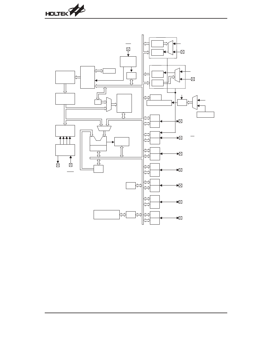
Block Diagram
HT48E70
Rev. 1.00
2
September 16, 2005
I N T
O S C 2
O S C 1
R E S
V D D
M U X
T M R 0 C
T M R 0 L
T M R 0 H
V S S
P r o g r a m
M e m o r y
P r o g r a m
C o u n t e r
I n t e r r u p t
C i r c u i t
S T A C K
I N T C
D A T A
M e m o r y
I n s t r u c t i o n
R e g i s t e r
M
U
X
I n s t r u c t i o n
D e c o d e r
S T A T U S
A L U
S h i f t e r
T i m i n g
G e n e r a t o r
A C C
M P
W D T S
W D T
W D T O S C
W D T P r e s c a l e r
M
U
X
E N / D I S
P D C
P O R T D
P G C
P G
P O R T G
P G 0 ~ P G 7
P O R T B
P B 0 / B Z
P B 1 / B Z
P B 2 ~ P B 7
P A C
P O R T A
T M R 1 C
T M R 1 L
T M R 1 H
M
U
X
T M R 1
f
S Y S
/ 4
P O R T E
P F C
P F
P O R T F
f
S Y S
/ 4
D a t a M e m o r y
E E P R O M
E E C R
B P
T M R 0
f
S Y S
/ 4
M
U
X
P O R T C
P C 0 ~ P C 7
P D 0 ~ P D 7
P E 0 ~ P E 7
P F 0 ~ P F 7
P E
P A 0 ~ P A 7
P E C
P D
P C
P C C
P B
P B C
P A
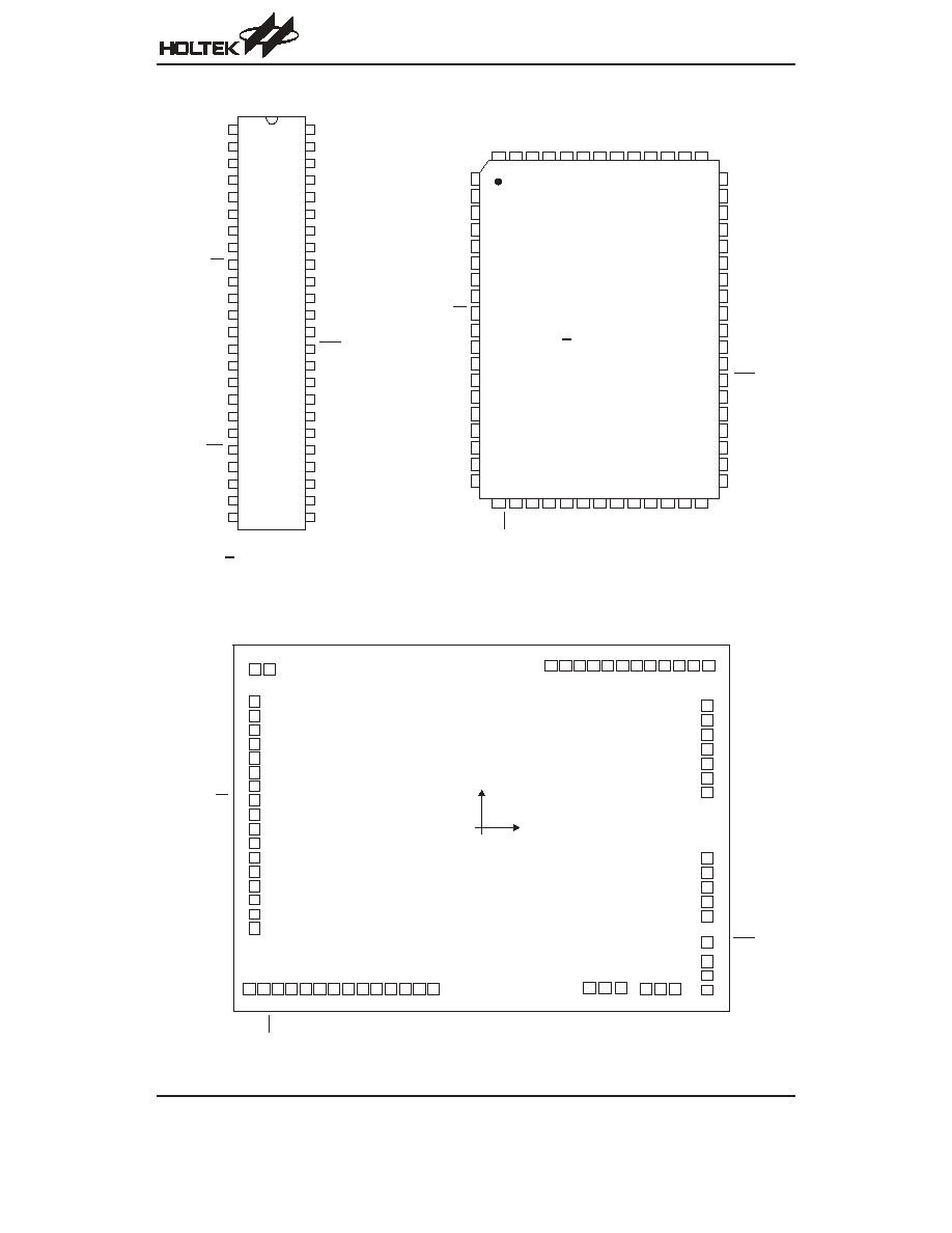
Pin Assignment
Pad Assignment
* The IC substrate should be connected to VSS in the PCB layout artwork.
HT48E70
Rev. 1.00
3
September 16, 2005
P B 6
P B 7
P A 4
P A 5
P A 6
P A 7
P F 0
P F 1
P F 2
P F 3
O S C 2
O S C 1
V D D
R E S
T M R 1
P D 3
P D 2
P D 1
P D 0
P C 7
P C 6
P C 5
P C 4
P C 3
P B 5
P B 4
P A 3
P A 2
P A 1
P A 0
P B 3
P B 2
P B 1 / B Z
P B 0 / B Z
P E 3
P E 2
P E 1
P E 0
P D 7
P D 6
P D 5
P D 4
V S S
I N T
T M R 0
P C 0
P C 1
P C 2
P
A
6
P
A
5
P
A
4
P
B
7
P
B
6
P
B
5
P
B
4
P
G
7
P
G
6
P
G
5
P
G
4
P
A
3
P
A
2
P A 7
P F 0
P F 1
P F 2
P F 3
O S C 2
O S C 1
P F 4
P F 5
P F 6
P F 7
V D D
R E S
T M R 1
P D 3
P D 2
P D 1
P D 0
P C 7
2 0 2 1 2 2 2 3 2 4
P A 1
P A 0
P E 7
P E 6
P E 5
P E 4
P B 3
P B 2
P B 1 / B Z
P B 0 / B Z
P E 3
P E 2
P E 1
P E 0
P D 7
P D 6
P D 5
P D 4
V S S
P
C
6
P
C
5
P
C
4
P
C
3
P
C
2
P
C
1
P
C
0
P
G
3
P
G
2
P
G
1
P
G
0
T
M
R
0
I
N
T
3 2
3 1
3 0
2 9
2 8
2 7
2 6
2 5
1
2
3
4
5
6
7
8
9
1 0
1 1
1 2
1 3
1 4
1 5
1 6
1 7
1 8
1 9
5 1
5 0
4 9
4 8
4 7
4 6
4 5
4 4
4 3
4 2
4 1
4 0
3 9
3 8
3 7
3 6
3 5
3 4
3 3
6 4 6 3 6 2 6 1 6 0
5 2
5 3
5 4
5 5
5 6
5 7
5 8
5 9
H T 4 8 E 7 0
4 8 S S O P - A
H T 4 8 E 7 0
6 4 Q F P - A
4 8
4 7
4 6
4 5
4 4
4 3
4 2
4 1
4 0
3 9
3 8
3 7
3 6
3 5
3 4
3 3
3 2
3 1
3 0
2 9
2 8
2 7
2 6
2 5
1
2
3
4
5
6
7
8
9
1 0
1 1
1 2
1 3
1 4
1 5
1 6
1 7
1 8
1 9
2 0
2 1
2 2
2 3
2 4
3 0 3 1 3 2
6 0
6 5 6 4
3 3 3 4 3 5
2 7
2 1
2 3
2 0
1 6 7
2
3
4
5
6
7
8
9
1 0
1 1
1 2
1 3
1 4
1 5
1 6
1 7
1 8
1 9
2 2
2 4 2 5 2 6
2 8 2 9
3 6 3 7 3 8
( 0 , 0 )
4 7
4 6
4 5
4 4
4 3
4 2
4 1
4 0
3 9
5 4
5 3
5 2
5 1
5 0
4 9
4 8
5 5
5 6
5 7
5 8
5 9
6 1
6 2
6 3
6 6
P A 0
P E 7
P E 6
P E 5
P E 4
P B 3
P B 2
P B 1 / B Z
P B 0 / B Z
P E 3
P E 2
P E 1
P E 0
P D 7
P D 6
P D 5
P D 4
P
A
1
V
S
S
I
N
T
T
M
R
0
P
G
0
P
G
1
P
G
2
P
G
3
P
C
0
P
C
1
P
C
2
P
C
3
P
C
4
P
C
5
P
C
6
P D 2
P
D
1
P
D
0
P
C
7
T
R
I
M
2
T
R
I
M
3
P A 7
P F 0
P F 1
P F 2
P F 3
O S C 2
O S C 1
P F 4
P F 5
P F 6
P F 7
V D D
R E S
T M R 1
P D 3
T
R
I
M
1
P
A
6
P
A
5
P
A
4
P
B
7
P
B
6
P
B
5
P
B
4
P
G
7
P
G
6
P
G
5
P
G
4
P
A
3
P
A
2
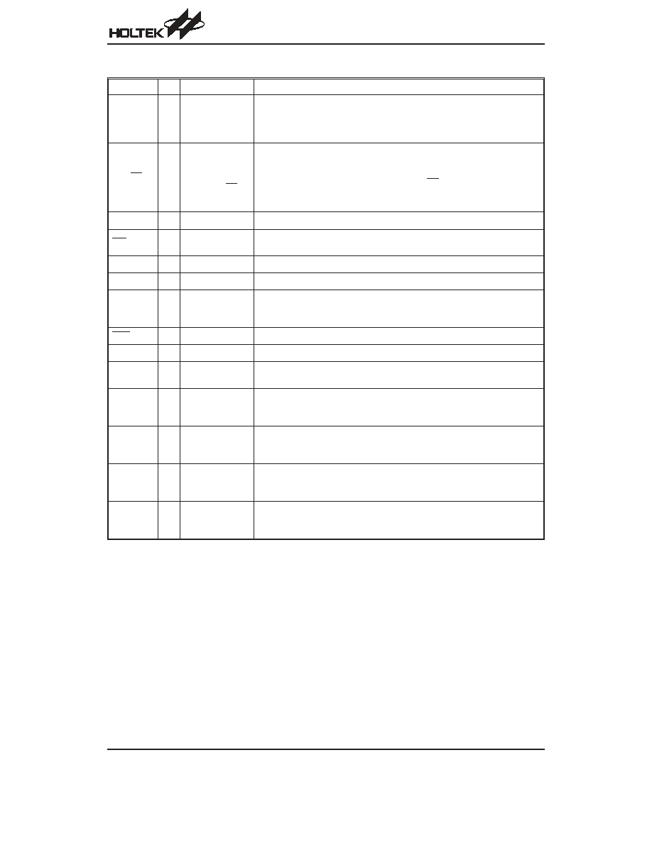
Pad Description
Pad Name
I/O
Options
Description
PA0~PA7
I/O
Wake-up
Pull-high*
CMOS or Schmitt
Input
Bidirectional 8-bit input/output port.
Each bit can be configured as a wake-up input by options. Software instruc-
tions determine if the pin is a CMOS output or Schmitt trigger input or CMOS
input with or without pull-high resistor (by options).
PB0/BZ
PB1/BZ
PB2~PB7
I/O
Pull-high*
PB0 or BZ
PB1 or BZ
Bidirectional 8-bit input/output port.
Software instructions determine if the pin is a CMOS output or Schmitt trigger
input with pull-high resistor (determined by pull-high options).
The PB0 and PB1 are pin-shared with BZ and BZ respectively. Once the PB0
or PB1 is selected as buzzer driving output, the output signals come from an
internal PFD generator (shared with timer/event counter).
VSS
¾
¾
Negative power supply, ground
INT
I
¾
External interrupt Schmitt trigger without pull-high resistor.
Edge trigger is activated during high to low transition.
TMR0
I
¾
Schmitt trigger input for Timer/Event Counter 0
TMR1
I
¾
Schmitt trigger input for Timer/Event Counter 1
PC0~PC7
I/O
Pull-high*
Bidirectional 8-bit input/output port.
Software instructions determine the CMOS output or Schmitt trigger input
(pull-high depends on options).
RES
I
¾
Schmitt trigger reset input, active low.
VDD
¾
¾
Positive power supply
OSC1
OSC2
I
O
Crystal
or RC
OSC1 and OSC2 are connected to an RC network. For RC operation, OSC2
is an output terminal for 1/4 system clock.
PD0~PD7
I/O
Pull-high*
Bidirectional 8-bit input/output port.
Software instructions determine if the pin is a CMOS output or Schmitt trigger
input (pull-high depends on options).
PE0~PE7
I/O
Pull-high*
Bidirectional 8-bit input/output port.
Software instructions determine if the pin is a CMOS output or Schmitt trigger
input (pull-high depends on options).
PF0~PF7
I/O
Pull-high*
Bidirectional 8-bit input/output port.
Software instructions determine if the pin is a CMOS output or Schmitt trigger
input (pull-high depends on options).
PG0~PG7
I/O
Pull-high*
Bidirectional 8-bit input/output port.
Software instructions determine if the pin is a CMOS output or Schmitt trigger
input (pull-high depends on options).
Note:
* The pull-high resistors of each I/O port (PA, PB, PC, PD, PE, PF, PG) are controlled by options.
CMOS or Schmitt trigger option of port A is controlled by an option.
Absolute Maximum Ratings
Supply Voltage ...........................V
SS
-0.3V to V
SS
+6.0V
Storage Temperature ............................
-50°C to 125°C
Input Voltage..............................V
SS
-0.3V to V
DD
+0.3V
Operating Temperature...........................
-40°C to 85°C
Note: These are stress ratings only. Stresses exceeding the range specified under
²Absolute Maximum Ratings² may
cause substantial damage to the device. Functional operation of this device at other conditions beyond those
listed in the specification is not implied and prolonged exposure to extreme conditions may affect device reliabil-
ity.
HT48E70
Rev. 1.00
4
September 16, 2005
D.C. Characteristics
Ta=25
°C
Symbol
Parameter
Test Conditions
Min.
Typ.
Max.
Unit
V
DD
Conditions
V
DD
Operating Voltage
¾ f
SYS
=4MHz
2.2
¾
5.5
V
¾ f
SYS
=8MHz
3.3
¾
5.5
V
I
DD1
Operating Current (Crystal OSC)
3V
No load, f
SYS
=4MHz
¾
1
2
mA
5V
¾
3
5
mA
I
DD2
Operating Current (RC OSC)
3V
No load, f
SYS
=4MHz
¾
1
2
mA
5V
¾
2.5
4
mA
I
DD3
Operating Current
(Crystal OSC, RC OSC)
5V No load, f
SYS
=8MHz
¾
4
8
mA
I
STB1
Standby Current (WDT Enabled)
3V
No load, system HALT
¾
¾
5
mA
5V
¾
¾
10
mA
I
STB2
Standby Current (WDT Disabled)
3V
No load, system HALT
¾
¾
1
mA
5V
¾
¾
2
mA
I
STB3
Standby Current (WDT Disabled)
3V
No load, system HALT
¾
¾
5
mA
5V
¾
¾
10
mA
V
IL1
Input Low Voltage for I/O Ports
¾
¾
0
¾
0.3V
DD
V
V
IH1
Input High Voltage for I/O Ports
¾
¾
0.7V
DD
¾
V
DD
V
V
IL2
Input Low Voltage (RES)
¾
¾
0
¾
0.4V
DD
V
V
IH2
Input High Voltage (RES)
¾
¾
0.9V
DD
¾
V
DD
V
V
LVR
Low Voltage Reset
¾ LVRenabled
2.7
3.0
3.3
V
I
OL
I/O Port Sink Current
3V V
OL
=0.1V
DD
4
8
¾
mA
5V V
OL
=0.1V
DD
10
20
¾
mA
I
OH
I/O Port Source Current
3V V
OH
=0.9V
DD
-2
-4
¾
mA
5V V
OH
=0.9V
DD
-5
-10
¾
mA
R
PH
Pull-high Resistance
3V
¾
20
60
100
k
W
5V
10
30
50
k
W
HT48E70
Rev. 1.00
5
September 16, 2005
Document Outline
- þÿ
- þÿ
- þÿ
- þÿ
- þÿ
- þÿ
- þÿ
- þÿ
- þÿ
- þÿ
- þÿ
- þÿ
- þÿ
- þÿ
- þÿ