 | ÐлекÑÑоннÑй компоненÑ: HT48RA3 | СкаÑаÑÑ:  PDF PDF  ZIP ZIP |
Äîêóìåíòàöèÿ è îïèñàíèÿ www.docs.chipfind.ru
HT48RA3
8-Bit Remote Type OTP MCU
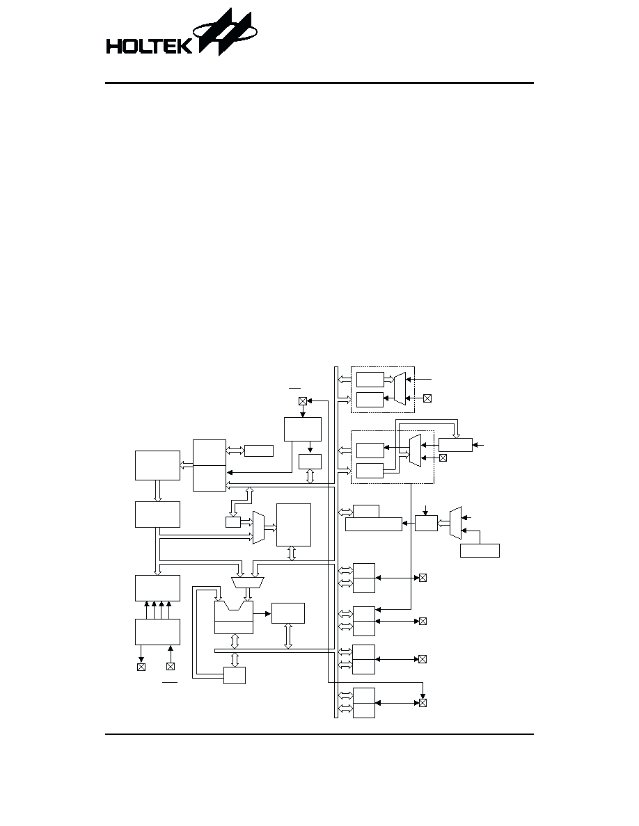
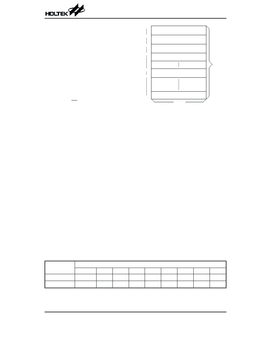
Block Diagram
Rev. 1.20
1
May 12, 2003
General Description
This device is an 8-bit high performance RISC-like MCU
designed for multiple I/O product applications. The de-
vice is particularly suitable for use in products such as
universal remote controller (URC). A HALT feature is in-
cluded to reduce power consumption. The data ROM
can be used to store codes of remote control.
Features
·
Operating voltage: 2.2V~3.6V
·
23 bidirectional I/O lines (max.)
·
1 interrupt input shared with an I/O line
·
8-bit programmable timer/event counter with overflow
interrupt and 8-stage prescaler (TMR0)
·
16-bit programmable timer/event counter and over-
flow interrupts (TMR1)
·
On-chip crystal and RC oscillator
·
Watchdog Timer
·
24K
´16 program memory EPROM
(8K
´16 bits´3 banks)
·
224
´8 data memory RAM
·
PFD supported
·
HALT function and wake-up feature reduce power
consumption
·
8-level subroutine nesting
·
Up to 1
ms instruction cycle with 4MHz system clock at
V
DD
=3V
·
Bit manipulation instruction
·
16-bit table read instruction
·
63 powerful instructions
·
All instructions in one or two machine cycles
·
28-pin SKDIP/SOP package
I N T / P . 0
O S C 2
O S C 1
R E S
V D D
M U X
T M R 0
T M R 0 C
T M R 0
V S S
P r e s c a l e r
f
S Y S
P r o g r a m
E P R O M
P r o g r a m
C o u n t e r
I n t e r r u p t
C i r c u i t
S T A C K
I N T C
D A T A
M e m o r y
I n s t r u c t i o n
R e g i s t e r
M
U
X
I n s t r u c t i o n
D e c o d e r
S T A T U S
A L U
S h i f t e r
T i m i n g
G e n e r a t o r
A C C
M
U
X
M P
W D T S
W D T
W D T O S C
W D T P r e s c a l e r
M
U
X
E N / D I S
P . C
P .
P O R T .
P . 0
P B C
P O R T B
P B 0 ~ P B 7
P . D
P B
P A C
P O R T A
P A 0 ~ P A 7
P A
P C
P O R T C
P C 0 ~ P C 5
P C C
T M R 1 C
T M R 1
M
U
X
T M R 1
f
S Y S
/ 4
B P
f
S Y S
/ 4
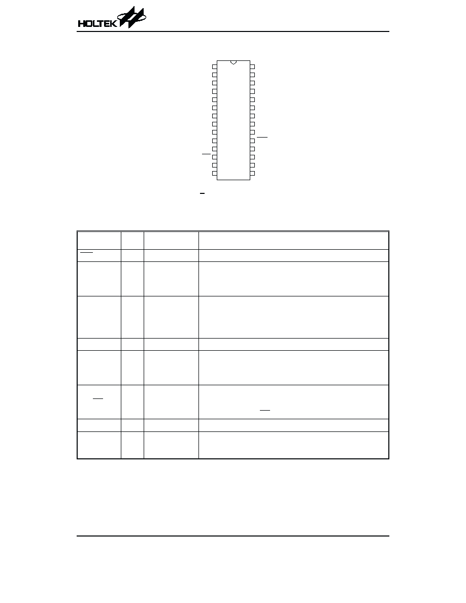
Pin Assignment
Pin Description
Pin Name
I/O
ROM Code
Option
Description
RES
I
¾
Schmitt trigger reset input, active low.
PA0~PA7
I/O
Wake-up*
Pull-high***
Bidirectional 8-bit input/output port. Each bit can be configured as a
wake-up input by a option. Software instructions determine the CMOS
output or Schmitt trigger input with/without pull-high resistor. The pull-high
resistor of each input/output line is also optional.
PB0/PFD
PB1~PB7
I/O
Pull-high**
PB0 or PFD
Bidirectional 8-bit input/output port. Software instructions determine
the CMOS output or Schmitt trigger input with/without pull-high resis-
tor. The pull-high resistor of each input/output line is also optional. The
output mode of PB0 can be used as an internal PFD signal output and
it can be used as a various frequency carrier signal.
VSS
¾
¾
Negative power supply, ground
PC0/TMR0
PC1~PC4
PC5/TMR1
I/O
Pull-high*
Bidirectional 6-bit input/output port. Software instructions determine
the CMOS output or Schmitt trigger input with/without pull-high resis-
tor. The pull-high resistor of each input/output line is also optional. PC0
and PC5 are pin shared with TMR0 and TMR1 function pins.
PF0/INT
I/O
Pull-high*
Bidirectional 1-bit input/output port. Software instructions determine
the CMOS output or Schmitt trigger input with/without pull-high resis-
tor. The pull-high resistor of this input/output line is also optional. PF0
is pin shared with the INT function pin.
VDD
¾
¾
Positive power supply
OSC1
OSC2
I
O
Crystal
or RC
OSC1, OSC2 are connected to an RC network or Crystal (determined
by option) for the internal system clock. In the case of RC operation,
OSC2 is the output terminal for 1/4 system clock.
Note:
*:
Bit option
**: Nibble option
***: Byte option
HT48RA3
Rev. 1.20
2
May 12, 2003
2 8
2 7
2 6
2 5
2 4
2 3
2 2
2 1
2 0
1 9
1 8
1 7
1 6
1 5
1
2
3
4
5
6
7
8
9
1 0
1 1
1 2
1 3
1 4
P B 6
P B 7
P A 4
P A 5
P A 6
P A 7
O S C 2
O S C 1
V D D
R E S
P C 5 / T M R 1
P C 4
P C 3
P C 2
P B 5
P B 4
P A 3
P A 2
P A 1
P A 0
P B 3
P B 2
P B 1
P B 0 / P . D
V S S
P . 0 / I N T
P C 0 / T M R 0
P C 1
H T 4 8 R A 3
2 8 S K D I P - A / S O P - A
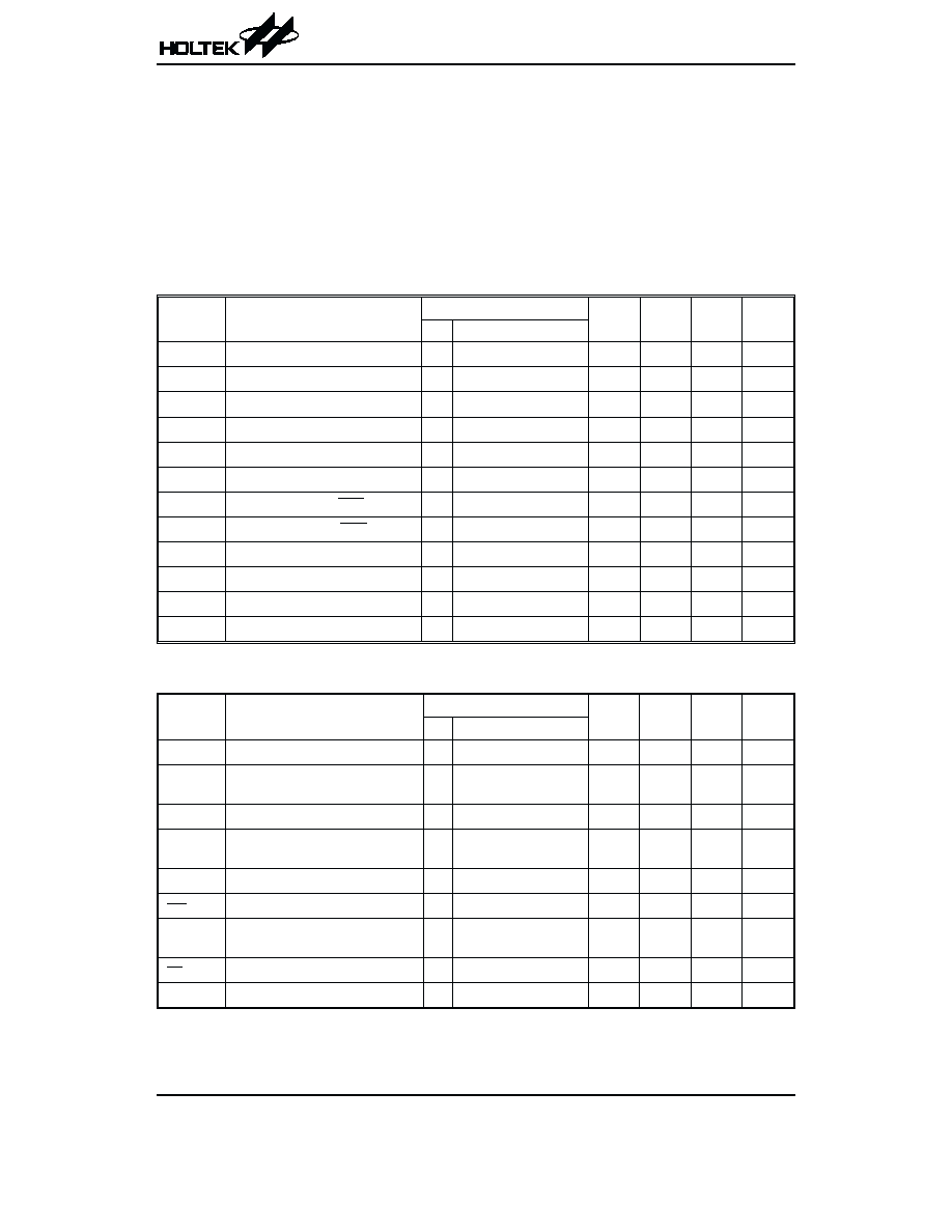
Absolute Maximum Ratings
Supply Voltage ...........................V
SS
-0.3V to V
SS
+5.5V
Storage Temperature ............................
-50°C to 125°C
Input Voltage..............................V
SS
-0.3V to V
DD
+0.3V
Operating Temperature...........................
-40°C to 85°C
Note: These are stress ratings only. Stresses exceeding the range specified under
²Absolute Maximum Ratings² may
cause substantial damage to the device. Functional operation of this device at other conditions beyond those
listed in the specification is not implied and prolonged exposure to extreme conditions may affect device reliabil-
ity.
D.C. Characteristics
Ta=25
°C
Symbol
Parameter
Test Conditions
Min.
Typ.
Max.
Unit
V
DD
Conditions
V
DD
Operating Voltage
¾
¾
2.2
¾
3.6
V
I
DD
Operating Current
3V
No load, f
SYS
=4MHz
¾
3
5
mA
I
STB1
Standby Current (WDT Enabled)
3V
No load, system HALT
¾
5
10
mA
I
STB2
Standby Current (WDT Disabled)
3V
No load, system HALT
¾
0.1
1
mA
V
IL1
Input Low Voltage for I/O Ports
¾
¾
0
¾
0.3V
DD
V
V
IH1
Input High Voltage for I/O Ports
¾
¾
0.7V
DD
¾
V
DD
V
V
IL2
Input Low Voltage (RES Ports)
¾
¾
0
¾
0.4V
DD
V
V
IH2
Input High Voltage (RES Ports)
¾
¾
0.9V
DD
¾
V
DD
V
I
OL
I/O Port Sink Current
3V
V
OL
=0.1V
DD
5
10
¾
mA
I
OH1
I/O Port Source Current
3V
V
OH
=0.9V
DD
-2
-5
¾
mA
I
OH2
I/O Port Source Current
3V
V
OH
=0.8V
DD
-4
-8
¾
mA
R
PH
Pull-high Resistance
3V
¾
40
60
80
k
W
A.C. Characteristics
Ta=25
°C
Symbol
Parameter
Test Conditions
Min.
Typ.
Max.
Unit
V
DD
Conditions
f
SYS
System Clock
3V
¾
400
¾
4000
kHz
f
TIMER
Timer I/P Frequency
(TMR0/TMR1)
3V
50% duty
0
¾
4000
kHz
t
WDTOSC
Watchdog Oscillator
3V
¾
45
90
180
ms
t
WDT1
Watchdog Time-out Period
(WDT OSC)
3V
Without WDT prescaler
11.5
23
46
ms
t
WDT2
Watchdog Time-out Period (f
SYS
/4) 3V
Without WDT prescaler
¾
1024
¾
t
SYS
t
RES
External Reset Low Pulse Width
¾
¾
1
¾
¾
ms
t
SST
System Start-up Timer Period
¾
Power-up, reset or
wake-up from HALT
¾
1024
¾
t
SYS
t
INT
Interrupt Pulse Width
¾
¾
1
¾
¾
ms
t
ACC
Data ROM Access Time
¾
¾
1
¾
¾
ms
Note: t
SYS
=1/(f
SYS
)
HT48RA3
Rev. 1.20
3
May 12, 2003
Functional Description
HT48RA3
Rev. 1.20
4
May 12, 2003
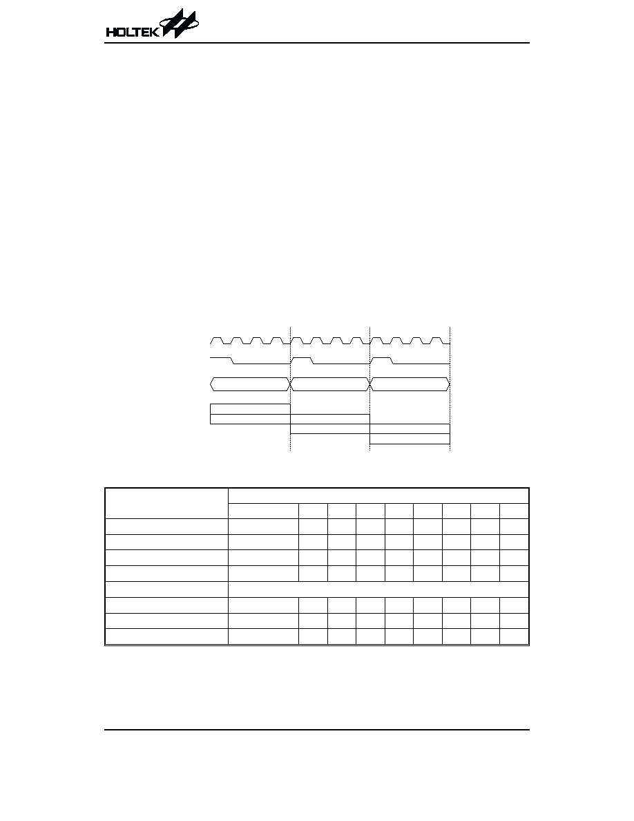
Execution Flow
The system clock for the MCU is derived from either a
crystal or an RC oscillator. The system clock is internally
divided into four non-overlapping clocks. One instruc-
tion cycle consists of four system clock cycles.
Instruction fetching and execution are pipelined in such
a way that a fetch takes an instruction cycle while de-
coding and execution takes the next instruction cycle.
However, the pipelining scheme causes each instruc-
tion to effectively execute in a cycle. If an instruction
changes the program counter, two cycles are required to
complete the instruction.
Program Counter
- PC
The program counter (PC) controls the sequence in
which the instructions stored in the program ROM are
executed and its contents specify a full range of pro-
gram memory.
After accessing a program memory word to fetch an in-
struction code, the contents of the program counter are
incremented by one. The program counter then points to
the memory word containing the next instruction code.
When executing a jump instruction, conditional skip ex-
ecution, loading register, subroutine call or return from
subroutine, initial reset, internal interrupt, external inter-
rupt or return from interrupts, the PC manipulates the
program transfer by loading the address corresponding
to each instruction.
The conditional skip is activated by instructions. Once
the condition is met, the next instruction, fetched during
the current instruction execution, is discarded and a
dummy cycle replaces it to get the proper instruction.
Otherwise proceed to the next instruction.
The lower byte of the program counter (PCL) is a read-
able and writeable register (06H). Moving data into the
PCL performs a short jump. The destination will be
within the current program ROM page.
When a control transfer takes place, an additional
dummy cycle is required.
T 1
T 2
T 3
T 4
T 1
T 2
T 3
T 4
T 1
T 2
T 3
T 4
. e t c h I N S T ( P C )
E x e c u t e I N S T ( P C - 1 )
. e t c h I N S T ( P C + 1 )
E x e c u t e I N S T ( P C )
. e t c h I N S T ( P C + 2 )
E x e c u t e I N S T ( P C + 1 )
P C
P C + 1
P C + 2
S y s t e m C l o c k
O S C 2 ( R C o n l y )
P C
Execution flow
Mode
Program Counter
*14~*8
*7
*6
*5
*4
*3
*2
*1
*0
Initial Reset
0000000
0
0
0
0
0
0
0
0
External Interrupt
0000000
0
0
0
0
0
1
0
0
Timer/Event Counter 0 Overflow
0000000
0
0
0
0
1
0
0
0
Timer/Event Counter 1 Overflow
0000000
0
0
0
0
1
1
0
0
Skip
*14~*13, (*12~*0+2): (within current bank)
Loading PCL
*14~*8
@7
@6
@5
@4
@3
@2
@1
@0
Jump, Call Branch
BP (5~6), #12~#8
#7
#6
#5
#4
#3
#2
#1
#0
Return (RET, RETI)
S14~S8
S7
S6
S5
S4
S3
S2
S1
S0
Program Counter
Note: *14~*0: Program counter bits
S14~S0: Stack register bits
#14~#0: Instruction code bits
@7~@0: PCL bits
1 bank: 8K words
HT48RA3
Rev. 1.20
5
May 12, 2003
Program Memory
- ROM
The program memory is used to store the program in-
structions which are to be executed. It also contains
data, table, and interrupt entries, and is organized into
8192
´16 bits´3 banks, addressed by the program coun-
ter and table pointer.
Certain locations in the program memory are reserved
for special usage:
·
Location 000H
This area is reserved for program initialization. After
chip reset, the program always begins execution at lo-
cation 000H.
·
Location 004H
This area is reserved for the external interrupt service
program. If the INT input pin is activated, the interrupt
is enabled and the stack is not full, the program begins
execution at location 004H.
·
Location 008H
This area is reserved for the Timer/Event Counter 0 in-
terrupt service program. If a timer interrupt results
from a Timer/Event Counter 0 overflow, and if the in-
terrupt is enabled and the stack is not full, the program
begins execution at location 008H .
·
Location 00CH
This location is reserved for the Timer/Event Counter
1 interrupt service program. If a timer interrupt results
from a Timer/Event Counter 1 overflow, and the inter-
rupt is enabled and the stack is not full, the program
begins execution at location 00CH.
·
Table location
Any location in the program memory can be used as
look-up tables. The instructions
²TABRDC [m]² (page
specified by TBHP) and
²TABRDL [m]² (the last page)
transfer the contents of the lower-order byte to the
specified data memory, and the higher-order byte to
TBLH (08H). The higher-order byte table pointer
TBHP (1FH) and lower-order byte table pointer TBLP
(07H) are read/write registers, which indicate the table
locations. Before accessing the table, the location has
to be placed in TBHP and TBLP. The TBLH is read
only and cannot be restored. If the main routine and
the ISR (interrupt service routine) both employ the ta-
ble read instruction, the contents of TBLH in the main
routine are likely to be changed by the table read in-
struction used in the ISR. Errors are thus brought
about. Given this, using the table read instruction in
the main routine and the ISR simultaneously should
be avoided. However, if the table read instruction has
to be applied in both main routine and the ISR, the in-
terrupt(s) is supposed to be disabled prior to the table
read instruction. It (They) will not be enabled until the
TBLH in the main routine has been backup. All table
related instructions require 2 cycles to complete the
operation.
Stack Register
- STACK
This is a special part of the memory which is used to
save the contents of the program counter (PC) only. The
stack is organized into 8 levels and is neither part of the
data nor part of the program space, and is neither read-
able nor writeable. The activated level is indexed by the
stack pointer (SP) and is neither readable nor writeable.
At a subroutine call or interrupt acknowledge signal, the
contents of the program counter are pushed onto the
stack. At the end of a subroutine or an interrupt routine,
signaled by a return instruction (RET or RETI), the pro-
gram counter is restored to its previous value from the
stack. After a chip reset, the SP will point to the top of the
stack.
If the stack is full and a non-masked interrupt takes
place, the interrupt request flag will be recorded but the
acknowledge signal will be inhibited. When the stack
1 6 b i t s
5 . . . H
n . . H
P r o g r a m
M e m o r y
D e v i c e I n i t i a l i z a t i o n P r o g r a m
E x t e r n a l I n t e r r u p t S u b r o u t i n e
T i m e r / E v e n t C o u n t e r 0
I n t e r r u p t S u b r o u t i n e
L o o k - u p T a b l e ( 2 5 6 w o r d s )
L o o k - u p T a b l e ( 2 5 6 w o r d s )
N o t e : n r a n g e s f r o m 0 t o 5 .
0 0 C H
n 0 0 H
0 0 8 H
0 0 4 H
0 0 0 H
T i m e r / E v e n t C o u n t e r 1
I n t e r r u p t S u b r o u t i n e
Program memory
Instruction
Table Location
*14~*8
*7
*6
*5
*4
*3
*2
*1
*0
TABRDC [m]
TBHP
@7
@6
@5
@4
@3
@2
@1
@0
TABRDL [m]
1011111
@7
@6
@5
@4
@3
@2
@1
@0
Table location
Note: *14~*0: Table location bits
@7~@0: Table pointer bits
Document Outline
- þÿ
- þÿ
- þÿ
- þÿ
- þÿ
- þÿ
- þÿ
- þÿ
- þÿ
- þÿ
- þÿ
- þÿ
- þÿ
- þÿ