 | –≠–ª–µ–∫—Ç—Ä–æ–Ω–Ω—ã–π –∫–æ–º–ø–æ–Ω–µ–Ω—Ç: HT49C30-1 | –°–∫–∞—á–∞—Ç—å:  PDF PDF  ZIP ZIP |
Document Outline
- ˛ˇ
- ˛ˇ
- ˛ˇ
- ˛ˇ
- ˛ˇ
- ˛ˇ
- ˛ˇ
- ˛ˇ
- ˛ˇ
- ˛ˇ
- ˛ˇ
- ˛ˇ
- ˛ˇ
- ˛ˇ
- ˛ˇ

HT49R30A-1/HT49C30-1/HT49C30L
8-Bit LCD Type MCU
Rev. 1.10
1
September 25, 2002
Features
∑
Operating voltage:
2.2V~5.5V for HT49R30A-1/HT49C30-1
1.2V~2.2V for HT49C30L
∑
6 input lines
∑
8 bidirectional I/O lines
∑
Two external interrupt input
∑
One 8-bit programmable timer/event counter with
PFD (programmable frequency divider) function
∑
LCD driver with 19
¥2, 19¥3 or 18¥4 segments
∑
2K
¥14 program memory ROM
∑
96
¥8 data memory RAM
∑
Real Time Clock (RTC)
∑
8-bit prescaler for RTC
∑
Watchdog Timer
∑
Buzzer output
∑
On-chip crystal, RC and 32768Hz crystal oscillator
∑
HALT function and wake-up feature reduce power
consumption
∑
4-level subroutine nesting
∑
Bit manipulation instruction
∑
14-bit table read instruction
∑
Up to 0.5
ms instruction cycle with 8MHz system clock
for HT49R30A-1/HT49C30-1
∑
Up to 8
ms instruction cycle with 500kHz system clock
for HT49C30L
∑
63 powerful instructions
∑
All instructions in 1 or 2 machine cycles
∑
Low voltage reset/detector for
HT49R30A-1/HT49C30-1
∑
48-pin SSOP package
General Description
The HT49C30-1 and the HT49C30L are 8-bit high per-
f o r m a n c e s i n g l e c h i p m i c r o c o n t r o l l e r s . T h e
HT49R30A-1 is the OTP version of the HT49C30-1. Its
single cycle instruction and two-stage pipeline architec-
ture make it suitable for high speed applications. The
devices are also suitable for use in multiple LCD low
power applications such as scales, leisure products,
high-level household appliances, hand held LCD prod-
ucts and batteries operated systems in particular.
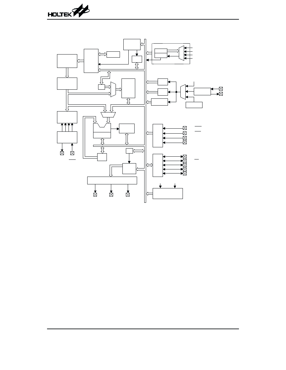
Block Diagram
HT49R30A-1/HT49C30-1/HT49C30L
Rev. 1.10
2
September 25, 2002
P r o g r a m
C o u n t e r
P r o g r a m
M e m o r y
I n s t r u c t i o n
R e g i s t e r
I n s t r u c t i o n
D e c o d e r
T i m i n g
G e n e r a t i o n
O S C 2
O S C 4
O S C 1
R E S
V D D
V S S
O S C 3
I n t e r r u p t
C i r c u i t
I N T C
M P
M
U
X
M U X
D A T A
M e m o r y
A L U
S h i f t e r
S T A T U S
A C C
P A
P O R T A
P A 0 / B Z
M
U
X
f
S Y S
/ 4
P B
P O R T B
P B 2 / T M R
W D T O S C
P A 1 / B Z
P A 2
P A 3 / P . D
P A 4 ~ P A 7
P B 0 / I N T 0
P B 1 / I N T 1
R T C O S C
O S C 3
O S C 4
R T C
S T A C K
L C D
M e m o r y
B P
L C D D R I V E R
C O M 0 ~
C O M 2
C O M 3 /
S E G 1 8
S E G 0 ~
S E G 1 7
T i m e B a s e
W D T
P B 3 ~ P B 5
H A L T
E N / D I S
L V D / L V R
T M R C
T M R
M
U
X
P . D
f
S Y S
/ 4
f
S Y S
R T C O u t
P B 2 / T M R

Pin Assignment
Pad Assignment
HT49C30-1
HT49R30A-1/HT49C30-1/HT49C30L
Rev. 1.10
3
September 25, 2002
4 8
4 7
4 6
4 5
4 4
4 3
4 2
4 1
4 0
3 9
3 8
3 7
3 6
3 5
3 4
3 3
3 2
3 1
3 0
2 9
2 8
2 7
2 6
2 5
1
2
3
4
5
6
7
8
9
1 0
1 1
1 2
1 3
1 4
1 5
1 6
1 7
1 8
1 9
2 0
2 1
2 2
2 3
2 4
P A 0 / B Z
P A 1 / B Z
P A 2
P A 3 / P . D
P A 4
P A 5
P A 6
P A 7
P B 0 / I N T 0
P B 1 / I N T 1
P B 2 / T M R
P B 3
P B 4
P B 5
V S S
V L C D
V 1
V 2
C 1
C 2
C O M 0
C O M 1
C O M 2
S E G 1 8 / C O M 3
R E S
O S C 1
O S C 2
V D D
O S C 3
O S C 4
S E G 0
S E G 1
S E G 2
S E G 3
S E G 4
S E G 5
S E G 6
S E G 7
S E G 8
S E G 9
S E G 1 0
S E G 1 1
S E G 1 2
S E G 1 3
S E G 1 4
S E G 1 5
S E G 1 6
S E G 1 7
H T 4 9 R 3 0 A - 1 / H T 4 9 C 3 0 - 1 / H T 4 9 C 3 0 L
4 8 S S O P - A
( 0 , 0 )
3 9
4 0
4 1
4 2
4 3
4 4
4 5
4 6
4 7
4 8
4 9
5 0
5 1
1
2
3
4
5
6
7
8
9
1 0
1 1
1 2
3 8
3 7
3 6
3 5
3 4
3 3
3 2
3 1
3 0
2 9
2 8
2 7
1 7 1 8 1 9
2 0
2 1 2 2 2 3 2 4 2 5 2 6
1 3 1 4 1 5 1 6
P
A
5
T
E
S
T
1
P A 6
P A 7
T M R / P B 2
P B 3
P B 4
P B 5
V S S
V L C D
I N T 0 / P B 0
I N T 1 / P B 1
S
E
G
1
2
S
E
G
1
3
S
E
G
1
4
S
E
G
1
5
S
E
G
1
6
S
E
G
1
7
S
E
G
1
8
/
C
O
M
3
C
O
M
2
C
O
M
1
C
O
M
0
C
2
C
1
V
2
V
1
S E G 5
S E G 6
S E G 7
S E G 8
S E G 9
S E G 1 0
S E G 1 1
S E G 4
S E G 3
S E G 2
S E G 1
S E G 0
O
S
C
4
O
S
C
3
V
D
D
O
S
C
2
O
S
C
1
B
Z
/
P
A
0
P
A
2
T
E
S
T
3
P
.
D
/
P
A
3
T
E
S
T
2
P
A
4
R
E
S
B
Z
/
P
A
1

HT49C30L
* The IC substrate should be connected to VSS in the PCB layout artwork.
Pad Description
Pad Name
I/O
Options
Description
PA0/BZ
PA1/BZ
PA2
PA3/PFD
PA4~PA7
I/O
Wake-up
Pull-high
or None
CMOS or
NMOS
PA0~PA7 constitute an 8-bit bidirectional input/output port with Schmitt trig-
ger input capability. Each bit on port can be configured as a wake-up input by
options. PA0~PA3 can be configured as a CMOS output or NMOS input/out-
put with or without pull-high resistor by options. PA4~PA7 are always
pull-high NMOS input/output. Of the eight bits, PA0~PA1 can be set as I/O
pins or buzzer outputs by options. PA3 can be set as an I/O pin or as a PFD
output also by options.
PB0/INT0
PB1/INT1
PB2/TMR
PB3~PB5
I
æ
PB0~PB5 constitute a 6-bit Schmitt trigger input port. Each bit on port are
with pull-high resistor. Of the six bits, PB0 and PB1 can be set as input pins or
as external interrupt control pins (INT0) and (INT1) respectively, by software
application. PB2 can be set as an input pin or as a timer/event counter input
pin TMR also by software application.
VSS
æ
æ
Negative power supply, ground
VLCD
I
æ
LCD power supply for HT49R30A-1/HT49C30-1.
Voltage pump for HT49C30L.
V2
I
æ
Voltage pump for HT49R30A-1/HT49C30-1.
LCD power supply for HT49C30L.
V1,C1,C2
I
æ
Voltage pump
SEG18/COM3
COM2~COM0
O
1/2 or 1/3 or 1/4
Duty
SEG18 can be set as a segment or as a common output driver for LCD panel
by options. COM2~COM0 are outputs for LCD panel plate.
SEG17~SEG0
O
æ
LCD driver outputs for LCD panel segments
HT49R30A-1/HT49C30-1/HT49C30L
Rev. 1.10
4
September 25, 2002
( 0 , 0 )
1 2
1 3 1 4
1 5
1 6 1 7 1 8 1 9 2 0 2 1 2 2 2 3 2 4 2 5
3 7
3 6
3 5
3 4
3 3
3 2
3 1
3 0
2 9
2 8
2 7
2 6
1
4 8 4 7 4 6 4 5 4 4 4 3
4 2
4 1
4 0 3 9 3 8
S
E
G
1
2
S
E
G
1
3
S
E
G
1
4
S
E
G
1
5
S
E
G
1
6
S
E
G
1
7
C
O
M
3
/
S
E
G
1
8
C
O
M
2
C
O
M
1
C
O
M
0
C
2
C
1
V
2
V
1
S E G 0
S E G 1
S E G 2
S E G 3
S E G 4
S E G 5
S E G 6
S E G 7
S E G 8
S E G 9
S E G 1 0
S E G 1 1
O
S
C
4
O
S
C
3
V
D
D
O
S
C
2
O
S
C
1
R
E
S
B
Z
/
P
A
0
B
Z
/
P
A
1
P
A
2
P
.
D
/
P
A
3
P
A
4
P
A
5
P A 6
P A 7
I N T 0 / P B 0
I N T 1 / P B 1
T M R / P B 2
P B 3
P B 4
P B 5
V S S
V L C D
2
3
4
5
6
7
8
9
1 0
1 1

Pad Name
I/O
Options
Description
OSC4
OSC3
O
I
RTC or
System Clock
Real time clock oscillators. OSC3 and OSC4 are connected to a 32768Hz
crystal oscillator for timing purposes or to a system clock source (depending
on the options).
VDD
æ
æ
Positive power supply
OSC2
OSC1
O
I
Crystal or RC
OSC1 and OSC2 are connected to an RC network or a crystal (by options)
for the internal system clock. In the case of RC operation, OSC2 is the output
terminal for 1/4 system clock.
The system clock may come from the RTC oscillator. If the system clock co-
mes from RTCOSC, these two pins can be floating.
RES
I
æ
Schmitt trigger reset input, active low
Absolute Maximum Ratings
Supply Voltage..................................V
SS
-0.3V to 5.5V*
Supply Voltage ................................V
SS
-0.3V to 2.2V**
Storage Temperature ............................
-50∞C to 125∞C
Input Voltage..............................V
SS
-0.3V to V
DD
+0.3V
Operating Temperature ...........................
-40∞C to 85∞C
Note: These are stress ratings only. Stresses exceeding the range specified under
≤Absolute Maximum Ratings≤ may
cause substantial damage to the device. Functional operation of this device at other conditions beyond those
listed in the specification is not implied and prolonged exposure to extreme conditions may affect device reliabil-
ity.
≤*≤ For HT49R30A-1/HT49C30-1
≤**≤ For HT49C30L
D.C. Characteristics
V
DD
=1.5V for HT49C30L, V
DD
=3V & V
DD
=5V for HT49R30A-1 and HT49C30-1
Ta=25
∞C
Symbol
Parameter
Test Conditions
Min.
Typ.
Max.
Unit
V
DD
Conditions
V
DD
Operating Voltage
æ
for HT49C30L
1.2
æ
2.2
V
LVR disable
(for HT49R30A-1/HT49C30-1)
2.2
æ
5.5
V
I
DD1
Operating Current
(Crystal OSC)
1.5V No load, f
SYS
=455kHz
æ
60
100
mA
3V
No load, f
SYS
=4MHz
æ
1
2
mA
5V
æ
3
5
mA
I
DD2
Operating Current
(RC OSC)
1.5V No load, f
SYS
=400kHz
æ
50
100
mA
3V
No load, f
SYS
=4MHz
æ
1
2
mA
5V
æ
3
5
mA
I
DD3
Operating Current
(f
SYS
=32768Hz)
1.5V
No load
æ
2.5
4
mA
3V
æ
0.3
0.6
mA
5V
æ
2
4
mA
I
STB1
Standby Current
(*f
S
=T1)
1.5V
No load, system HALT,
LCD off at HALT
æ
0.1
0.5
mA
3V
æ
æ
1
mA
5V
æ
æ
2
mA
HT49R30A-1/HT49C30-1/HT49C30L
Rev. 1.10
5
September 25, 2002