 | –≠–ª–µ–∫—Ç—Ä–æ–Ω–Ω—ã–π –∫–æ–º–ø–æ–Ω–µ–Ω—Ç: HT6222 | –°–∫–∞—á–∞—Ç—å:  PDF PDF  ZIP ZIP |
Document Outline
- ˛ˇ
- ˛ˇ
- ˛ˇ
- ˛ˇ
- ˛ˇ
- ˛ˇ
- ˛ˇ
- ˛ˇ
- ˛ˇ
- ˛ˇ
- ˛ˇ
- ˛ˇ
HT6221/HT6222
Multi-Purpose Encoders
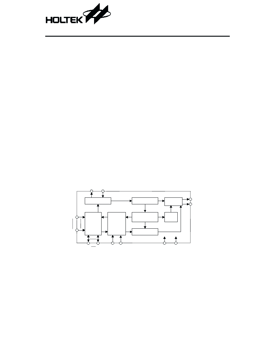
Block Diagram
1
March 2, 2000
Features
∑
Operating voltage: 1.8V~3.5V
∑
DOUT with 38kHz carrier for IR medium
∑
Low standby current
∑
Minimum transmission word: one word
∑
455kHz ceramic resonator or crystal
∑
16-bit address codes
∑
8-bit data codes
∑
PPM code method
∑
Three double-active keys
∑
Maximum active keys
-
HT6221: 32 keys
-
HT6222: 64 keys
∑
Low power and high noise immunity
CMOS technology
Applications
∑
Television and video cassette recorder con-
trollers
∑
Burglar alarm systems
∑
Smoke and fire alarm systems
∑
Garage door controllers
∑
Car door controllers
∑
Car alarm systems
∑
Security systems
∑
Other remote control systems
General Description
The HT6221/HT6222 are CMOS LSI encoders
designed for use in remote control systems. They
are capable of encoding 16-bit address codes and
8-bit data codes. Each address/data input can be
set to one of the two logic states, 0 and 1.
The HT6221/HT6222 contain 32 keys
(K1~K32) and 64 keys (K1~K64), respectively.
When one of the keys is triggered, the pro-
grammed address/data is transmitted together
with the header bits via an IR (38kHz carrier)
transmission medium.
O s c i l l a t o r
D i v i d e r
V D D
V S S
K e y b o a r d
M a t r i x &
G a t e
C i r c u i t
∏ 2 4 C o u n t e r &
1 o f 2 4 D e c o d e r
B i n a r y D e t e c t o r
D O U T
D a t a S e l e c t
& B u f f e r
S y n c .
C i r c u i t
X 2
X 1
R 1
R 8
D a t a R O M
& R e g i s t e r s
C 1
C 8
A I N
D 7
L E D

Pin Assignment
Pad Assignment
Chip size: 94 ¥ 104 (mil)
2
* The IC substrate should be connected to VDD in the PCB layout artwork.
HT6221/HT6222
2
March 2, 2000
2 4
2 3
2 2
2 1
2 0
1 9
1 8
1 7
1 6
1 5
1 4
1 3
1
2
3
4
5
6
7
8
9
1 0
1 1
1 2
2 0
1 9
1 8
1 7
1 6
1 5
1 4
1 3
1 2
1 1
1
2
3
4
5
6
7
8
9
1 0
A I N
C 1
C 2
C 3
C 4
C 5
C 6
C 7
C 8
L E D
R 1
R 2
R 3
R 4
D O U T
V D D
D 7
X 2
X 1
V S S
H T 6 2 2 1
2 0 D I P / S O P
H T 6 2 2 2
2 4 D I P / S O P
R 2
R 1
A I N
C 1
C 2
C 3
C 4
C 5
C 6
C 7
C 8
L E D
R 3
R 4
R 5
R 6
R 7
R 8
D O U T
V D D
D 7
X 2
X 1
V S S
1
1 3
2
1 4
3
1 5
4
1 6
5
1 7
6
1 8
7
1 9
8
2 0
9
2 1
1 0
2 2
1 1
2 3
1 2
2 4
K I 4
K I 5
K I 6
K I 7
R E M
V D D
S E L
O S C O
OS
C
I
VSS
LM
B
KI
O
7
KI
O
6
K I O 5
K I O 4
K I O 3
K I O 2
K I O 1
K I O 0
CC
S
KI
0
KI
1
KI
2
KI
3
( 0 , 0 )

Pad Coordinates
Unit: mil
Pad No.
X
Y
Pad No.
X
Y
1
-41.99
34.43
13
34.17
-46.88
2
-41.99
22.02
14
41.95
-30.26
3
-41.99
15.39
15
41.95
-13.98
4
-41.99
2.98
16
41.95
-4.12
5
-41.99
-5.61
17
41.95
12.16
6
-41.99
-28.31
18
41.95
22.02
7
-41.99
-37.83
19
39.99
46.84
8
-41.99
-46.88
20
28.26
46.84
9
-20.95
-46.88
21
-11.18
46.84
10
-14.32
-46.88
22
-23.16
46.84
11
-4.25
-46.88
23
-29.79
46.84
12
24.31
-46.88
24
-39.27
46.84
Pin Description
HT6222
Pin No. Pin Name I/O
Internal
Connection
Description
1~6
R3~R8
I
CMOS IN
Pull-low
Row control for keyboard matrix, active high
7
DOUT
O
CMOS OUT
Serial data output pin, with a 38kHz carrier
8
VDD
æ
æ
Positive power supply, 1.8V~3.5V for normal
operation
9
D7
I
CMOS IN
Most significant data bit (D7) code setting
10
X2
O
OSCILLATOR
455kHz resonator oscillator output
11
X1
I
OSCILLATOR
455kHz resonator oscillator input
12
VSS
æ
æ
Negative power supply
13
LED
O
CMOS OUT
Transmission enable indicator output
14~21
C8~C1
I/O
CMOS IN/OUT
Pull-low
Column control for keyboard matrix
22
AIN
I
CMOS IN
Pull-high
Pull-low
Low byte address codes (8 bits) scan input
23~24
R1~R2
I
CMOS IN
Pull-low
Row control for keyboard matrix, active high
HT6221/HT6222
3
March 2, 2000

Approximate internal connection circuits
Absolute Maximum Ratings
Supply Voltage.................................-0.3V to 6V
Storage Temperature.................-50∞C to 125∞C
Input Voltage.................V
SS
-0.3V to V
DD
+0.3V
Operating Temperature ..............-20∞C to 75∞C
Note: These are stress ratings only. Stresses exceeding the range specified under "Absolute Maxi-
mum Ratings" may cause substantial damage to the device. Functional operation of this device
at other conditions beyond those listed in the specification is not implied and prolonged expo-
sure to extreme conditions may affect device reliability.
Electrical Characteristic
Ta=25∞C
Symbol
Parameter
Test Conditions
Min. Typ. Max. Unit
V
DD
Conditions
V
DD
Operating Voltage
æ
æ
1.8
3
3.5
V
I
STB
Standby Current
3V Oscillator stops
æ
0.1
1.0
mA
I
DD
Operating Current
3V f
OSC
=455kHz
No load
æ
200
400
mA
I
OH1
Output Source Current for DOUT
3V V
O
=2.7V
-2.0 -4.0
æ
mA
I
OL1
Output Sink Current for DOUT
3V V
O
=0.3V
50
100
æ
mA
I
OH2
Output Source Current for LED
3V V
O
=2.7V
-10
-60
æ
mA
I
OL2
Output Sink Current for LED
3V V
O
=0.3V
1.2
2.0
æ
mA
I
OH3
Output Source Current for C1~C8
3V V
O
=2.7V
-0.6 -2.0
æ
mA
HT6221/HT6222
4
March 2, 2000
V
D D
C M O S I N / O U T
C M O S I N
P u l l - l o w
C M O S I N
O S C I L L A T O R
X 1
X 2
E N
1 0 M W
C M O S O U T
V
D D
C M O S I N / O U T
P u l l - l o w

Symbol
Parameter
Test Conditions
Min. Typ. Max. Unit
V
DD
Conditions
I
OL3
Output Sink Current for C1~C8
3V V
O
=0.3V
10
30
æ
mA
V
IH1
Input High Voltage for R1~R8
3V
æ
1.9
æ
3.0
V
V
IL1
Input Low Voltage for R1~R8
3V
æ
0
æ
0.8
V
V
IH2
Input High Voltage for C1~C8
3V
æ
1.1
æ
3.0
V
V
IL2
Input Low Voltage for C1~C8
3V
æ
0
æ
0.6
V
V
IH3
Input High Voltage for AIN
3V
æ
1.25
æ
3.0
V
V
IL3
Input Low Voltage for AIN
3V
æ
0
æ
0.6
V
R
PH1
Input Pull-high Resistance for AIN
3V V
IN
=0V
100
200
400
kW
R
PL1
Input Pull-low Resistance for AIN
3V V
IN
=3V
70
150
250
kW
R
PL2
Input Pull-low Resistance for R1~R8 3V V
IN
=3V
120
200
320
kW
R
PL3
Input Pull-low Resistance for C1~C8 3V V
IN
=3V
300
500 1500 kW
f
OSC
System Frequency
æ 455kHz ceramic
resonator
æ
455
æ
kHz
HT6221/HT6222
5
March 2, 2000
Functional Description
Keyboard scan
The HT6221/HT6222 remain in the halt mode
during the standby state (at this time, the oscil-
lator stops, and the standby current<1mA). The
HT6221 consists of 32 active keys, and the
HT6222 has 64 active keys. The keyboard
forms of the HT6221/ HT6222 are shown below.
∑
The HT6221 keyboard form
∑
The HT6222 keyboard form
C 1
R 1
R 2
R 3
R 4
R 5
R 6
R 7
R 8
K 1
K 2
K 3
K 4
K 3 3
K 3 4
K 3 5
K 3 6
K 5
K 6
K 7
K 8
K 3 7
K 3 8
K 3 9
K 4 0
K 9
K 1 0
K 1 1
K 1 2
K 4 1
K 4 2
K 4 3
K 4 4
K 1 3
K 1 4
K 1 5
K 1 6
K 4 5
K 4 6
K 4 7
K 4 8
K 1 7
K 1 8
K 1 9
K 2 0
K 4 9
K 5 0
K 5 1
K 5 2
K 2 1
K 2 2
K 2 3
K 2 4
K 5 3
K 5 4
K 5 5
K 5 6
K 2 9
K 3 0
K 3 1
K 3 2
K 6 1
K 6 2
K 6 3
K 6 4
K 2 5
K 2 6
K 2 7
K 2 8
K 5 7
K 5 8
K 5 9
K 6 0
C 2
C 3
C 4
C 5
C 6
C 7
C 8
K 1
K 2
K 3
K 4
K 5
K 6
K 7
K 8
K 9
K 1 0
K 1 1
K 1 2
K 1 3
K 1 4
K 1 5
K 1 6
C 1
C 2
C 3
C 4
R 1
R 2
R 3
R 4
K 1 7
K 1 8
K 1 9
K 2 0
K 2 1
K 2 2
K 2 3
K 2 4
K 2 5
K 2 6
K 2 7
K 2 8
K 2 9
K 3 0
K 3 1
K 3 2
C 5
C 6
C 7
C 8