Document Outline
- ˛ˇ
- ˛ˇ
- ˛ˇ
- ˛ˇ
- ˛ˇ
- ˛ˇ
- ˛ˇ
- ˛ˇ
- ˛ˇ
- ˛ˇ
- ˛ˇ
- ˛ˇ
- ˛ˇ
HT6240-002
Infrared Remote Encoder
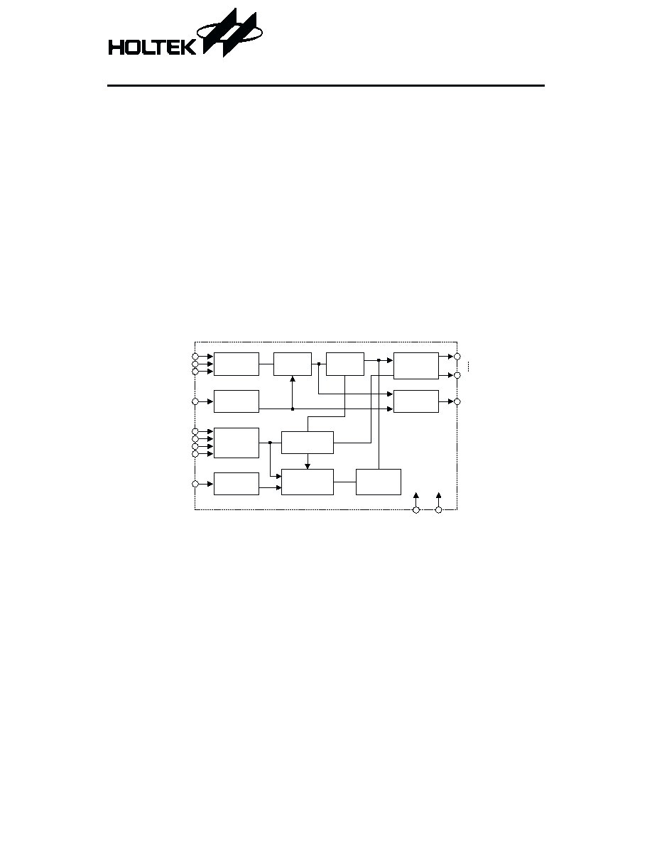
Block Diagram
1
December 16, 1999
Features
∑
Operating voltage: 2.2V~3.6V
∑
Low power consumption
∑
Few external parts
∑
20-pin DIP/SOP package
24-pin SOP package
Applications
∑
Television and video cassette recorder
controllers
∑
Garage door controllers
∑
Car door controllers
∑
Security systems
∑
Other remote control systems
General Description
HT6240-002 is designed as infrared remote
encoders, usually applied to TV systems. The
4¥8 key matrix input and the extension bit in-
put can transmit a max. of 256 instructions.
HT6240-002 have three different packages:
20-pin DIP, 20-pin SOP and 24-pin SOP.
3 ¥ 2
D u t y 1 / 3
2
1 0 ¥ 2
D i v i d e r
8
T E S T
M O D E
O S C
T E S T
V D D
V S S
P R B
O S C I
O S C O
C o n t r o l
U n i t
C u s t o m C o d e
& D A T A C o d e
L a t c h
K e y S c a n
D r i v e r
D e c o d e r
O u t p u t
S t a g e
O F 0
O F 7
I E - K E Y
E n c o d e r
8 - B i t S h i f t
R e g i s t e r
D A T A
I E 0
I E 1
I E 2
I E 3
P a r a l l e l t o
S e r i a l
C o n v e r t e r
C T

Pin Assignment
Pad Assignment
Chip size: 92 ¥ 118 mil
2
* The IC substrate should be connected to VDD in the PCB layout artwork.
HT6240-002
2
December 16, 1999
1
1 1
2
1 2
3
1 3
4
1 4
5
1 5
6
1 6
7
1 7
8
1 8
9
1 9
1 0
2 0
P R B
O S C I
O S C O
D A T E
I E 0
I E 1
IE
2
IE
3
OF
7
OF
6
O F 5
O F 4
O F 3
O F 1
O F 2
O F 0
CT
VD
D
VS
S
TE
S
T
( 0 , 0 )
2 4
2 3
2 2
2 1
2 0
1 9
1 8
1 7
1 6
1 5
1 4
1 3
1
2
3
4
5
6
7
8
9
1 0
1 1
1 2
2 0
1 9
1 8
1 7
1 6
1 5
1 4
1 3
1 2
1 1
1
2
3
4
5
6
7
8
9
1 0
V D D
C T
O F 0
O F 1
O F 2
O F 3
O F 4
O F 5
O F 6
O F 7
V S S
T E S T
P R B
O S C I
O S C O
D A T A
I E 0
I E 1
I E 2
I E 3
H T 6 2 4 0 - 0 0 2
2 0 D I P / S O P
V D D
C T
O F 0
O F 1
O F 2
O F 3
O F 4
O F 5
O F 6
O F 7
N C
N C
V S S
T E S T
P R B
O S C I
O S C O
D A T A
I E 0
I E 1
I E 2
I E 3
N C
N C
H T 6 2 4 0 - 0 0 2
2 4 S O P

Pad Coordinates
Unit: mil
Pad No.
X
Y
Pad No.
X
Y
1
-40.88
16.11
11
40.12
-48.32
2
-40.88
9.48
12
40.12
-39.74
3
-40.88
-11.56
13
40.12
-24.57
4
-40.88
-24.78
14
40.12
-15.98
5
-40.88
-34.04
15
40.12
-0.81
6
-40.88
-41.18
16
40.12
7.78
7
-13.77
-52.78
17
34.47
53.59
8
-7.14
-52.78
18
-8.97
53.59
9
9.22
-53.55
19
-15.60
53.59
10
24.40
-53.55
20
-22.23
52.02
Pad Description
Pad No.
Pad Name
I/O
Internal
Connection
Description
1
PRB
I
CMOS
Pull-high
Power on reset
2
OSCI
I
CMOS
Oscillator input
3
OSCO
O
CMOS
Oscillator output
4
DATA
I/O
CMOS, NMOS
Pull-high
Detect custom code and extended code
5~8
IE0~IE3
I
CMOS
Pull-high
Detect input from key matrix
9~16
OF7~OF0
O
NMOS
Drive for key scan
17
CT
O
CMOS
Generates output transmission code
18
VDD
æ
æ
Positive power supply
19
VSS
æ
æ
Negative power supply
20
TEST
I
CMOS
TEST=Low normal mode
TEST=High test mode
HT6240-002
3
December 16, 1999

Approximate internal connection circuits
Absolute Maximum Ratings
Supply Voltage..............................-0.3V to 5.2V
Input Voltage ......................V
SS
-0.3 to V
DD
+0.3
Output Voltage..................................V
SS
to V
DD
Storage Temperature.................-40∞C to 125∞C
Operating Temperature...............-20∞C to 70∞C
Note: These are stress ratings only. Stresses exceeding the range specified under ≤Absolute Maxi-
mum Ratings≤ may cause substantial damage to the device. Functional operation of this de-
vice at other conditions beyond those listed in the specification is not implied and prolonged
exposure to extreme conditions may affect device reliability.
HT6240-002
4
December 16, 1999
P i n : T E S T , O S C I
P i n : P R B , I E 0 ~ I E 3
I n p u t t e r m i n a l
V
D D
V
D D
V
D D
P i n : O S C O , C T
P i n : O F 0 ~ O F 7
O u t p u t t e r m i n a l
V
D D
P i n : D A T A
B i d i r e c t i o n a l t e r m i n a l
V
D D

Recommended Operating Condition
Ta=-20∞C~70∞C, unless otherwise noted
Symbol
Parameter
Test Conditions
Min.
Typ.
Max. Unit
V
DD
Conditions
V
DD
Supply Voltage
æ
æ
2.2
æ
3.6
V
V
IH
High-level Input Voltage
IE0~IE3, DATA
3V
æ
2.4V
3V
3V
V
High-level Voltage PRB
3V
æ
2.1V
3V
3V
V
IL
Low-level Input Voltage
IE0~IE3, DATA
3V
æ
0
0
1.2V
V
Low-level Input Voltage PRB
3V
æ
0
0
0.9V
f
OSC
Clock Oscillating Frequency
3V
æ
æ
455
æ
kHz
Electric Characteristics
Ta=25∞C, V
DD
=3V, V
SS
=0V, unless otherwise noted
Symbol
Parameter
Test Conditions
Limits
Unit
V
DD
Conditions
Min. Typ. Max.
V
DD
Supply Voltage
æ
f
OSC
=455kHz,
Ta=-20∞C~70∞C
2.2
æ
3.6
V
I
DD
Supply Current (during operation)
3V f
OSC
=455kHz
æ
0.1
0.3
mA
I
DD
Supply Current
(while not in operation)
3V
æ
æ
æ
1
mA
I
OH
High-level Output Current CT
3V V
OH
=2V
-5
-10
æ
mA
I
OL
Low-level Output Current CT
3V V
OL
=0.9V
0.3
0.8
æ
mA
Low-level Output Current DATA
3V V
OL
=0.9V
1
4
æ
Low-level Output Current
OF0~OF7
3V V
OL
=0.9V
1
4
æ
R
I
Pull-up Resistance PRB
3V
æ
æ
80
æ
kW
Pull-up Resistance DATA
3V
æ
æ
70
æ
Pull-up Resistance E0~E3
3V
æ
æ
70
æ
HT6240-002
5
December 16, 1999