Äîêóìåíòàöèÿ è îïèñàíèÿ www.docs.chipfind.ru
HT62L256
CMOS 32K´8 Low Power SRAM
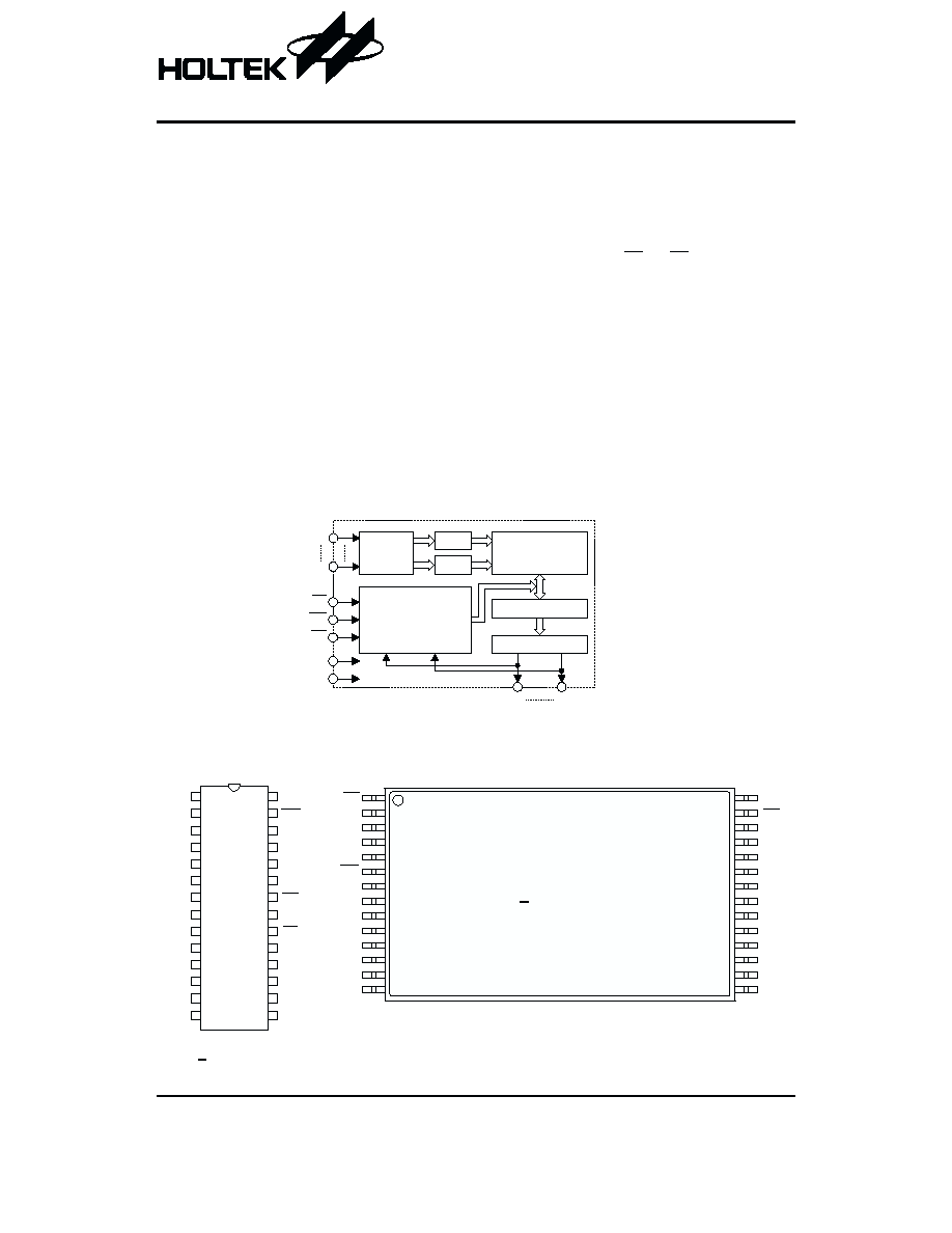
Block Diagram
Pin Assignment
Rev. 0.00
1
August 15, 2002
Features
·
Operation voltage: 2.7V~3.3V
·
Low power consumption:
-
Operating current: 20mA max.
-
Standby current: 2
mA
·
High speed access time: 70ns
·
Input levels are LVTTL-compatible
·
Automatic power down when chip is deselected
·
Three state outputs
·
Fully static operation
·
Data retention supply voltage as low as 2.0V
·
Easy expansion with CS and OE options
·
28-pin SOP/TSOP package
General Description
The HT62L256 is a 262,144-bit static random access
memory organized into 32,768 words by 8 bits and oper-
ating from a low power range of 2.7V to 3.3V supply volt-
age. It is fabricated with high performance CMOS
process that provides both high speed and low power
feature with typical standby current of 2
mA and maxi-
mum access time of 70ns.
The HT62L256 has an automatic power down feature,
reducing the power consumption significantly when chip
is deselected. The HT62L256 supports the JEDEC
standard 28-pin SOP and TSOP package.
A d d r e s s
B u f f e r s
R e a d / W r i t e
C o n t r o l L o g i c
V D D
V S S
W E
O E
C S
A 0
A 1 4
X - D e c
Y - D e c
M e m o r y C e l l A r r a y
( 3 2 K ´ 8 B i t s
S e n s e A m p l i f i e r
O u t p u t B u f f e r s
D 0
D 7
Preliminary
O E
A 1 1
A 9
A 8
A 1 3
W E
V D D
A 1 4
A 1 2
A 7
A 6
A 5
A 4
A 3
A 1 0
C S
D 7
D 6
D 5
D 4
D 3
V S S
D 2
D 1
D 0
A 0
A 1
A 2
1
1 4
1 5
2 8
H T 6 2 L 2 5 6
2 8 S O P - A
A 1 4
A 1 2
A 7
A 6
A 5
A 4
A 3
A 2
A 1
A 0
D 0
D 1
D 2
V S S
V D D
W E
A 1 3
A 8
A 9
A 1 1
O E
A 1 0
C S
D 7
D 6
D 5
D 4
D 3
2 8
2 7
2 6
2 5
2 4
2 3
2 2
2 1
2 0
1 9
1 8
1 7
1 6
1 5
1
2
3
4
5
6
7
8
9
1 0
1 1
1 2
1 3
1 4
H T 6 2 L 2 5 6
2 8 T S O P - A
Pin Description
Pin Name
I/O
Description
A0~A14
I
Address input pins
WE
I
Write enable signal pin, active LOW
OE
I
Output enable signal pin, active LOW
CS
I
Chip select signal pin, active LOW
D0~D7
I/O
Data input and output signal pins
VDD
¾
Positive power supply
VSS
¾
Negative power supply, ground
Absolute Maximum Rating
V
DD
to VSS ...........................................
-0.5V to +3.6V
Operating Temperature, T
OP
......................0
°C to 70°C
IN, IN/OUT Voltage to V
SS
.............
-0.5V to V
DD
+0.5V
Storage Temperature (Plastic), Tstg ...
-55°C to 125°C
Power Consumption, PT .......................................0.7W
Note: These are stress ratings only. Stresses exceeding the range specified under
²Absolute Maximum Ratings² may
cause substantial damage to the device. Functional operation of this device at other conditions beyond those
listed in the specification is not implied and prolonged exposure to extreme conditions may affect device reliabil-
ity.
D.C. Characteristics
Ta=25
°C, V
DD
=3.0V
±10%, T
OP
=0
°C to 70°C
Symbol
Parameter
Test Conditions
Min.
Typ.
Max.
Unit
V
DD
Operating Voltage
¾
2.7
3.0
3.3
V
V
IL
Input Low Voltage
¾
¾
0
0.4
V
V
IH
Input High Voltage
¾
0.7
´V
DD
¾
V
I
LI
Input Leakage Current
V
IN
=0 to V
DD
¾
¾
1
mA
I
LO
Output Leakage Current
CS=V
IH
or OE=V
IH
,
V
OUT
=0 to V
DD
¾
¾
1
mA
V
OL
Output Low Voltage
V
DD
=Max, I
OL
=2mA
¾
¾
0.3
V
V
OH
Output High Voltage
V
DD
=Min, I
OH
=
-1mA
V
DD
-0.3
¾
¾
V
I
DD
Operating Current
CS=V
IH
, I
OUT
=0mA
¾
¾
20
mA
I
SB1
Standby Current
CS=V
IH
, I
OUT
=0mA
¾
¾
50
mA
I
SB2
Power Down Supply Current
CS
³ V
DD
- 0.2V, V
IN
³0V
¾
2
10
mA
HT62L256
Rev. 0.00
2
August 15, 2002
Preliminary
A.C. Characteristics
Ta=25
°C, V
DD
=3.0V
±10%
Symbol
Parameter
Min.
Typ.
Max.
Unit
Read cycle
t
RC
Read Cycle Time
70
¾
¾
ns
t
AA
Address Access Time
¾
¾
70
ns
t
ACS
Chip Selection Access Time
¾
¾
70
ns
t
AOE
Output Enable to Valid Outputs
¾
¾
35
ns
t
CLZ*
Chip Selection to Output in Low-Z
10
¾
¾
ns
t
OLZ
*
Output Enabled to Output in Low-Z
5
¾
¾
ns
t
CHZ
*
Chip Deselected to Output in High-Z
¾
¾
25
ns
t
OHZ
*
Output Disable to Output in High-Z
¾
¾
25
ns
t
OH
Output Hold from Address Change
10
¾
¾
ns
Write cycle
t
WC
Write Cycle Time
70
¾
¾
ns
t
CW
Chip Selection to End of Write
60
¾
¾
ns
t
AS
Address Setup Time
0
¾
¾
ns
t
AW
Address Valid to End of Write
60
¾
¾
ns
t
WP
Write Pulse Width
50
¾
¾
ns
t
WR
Write Recovery Time
0
¾
¾
ns
t
WHZ
Write to Output in High
-Z
¾
¾
20
ns
t
DW
Data Valid to End of Write
30
¾
¾
ns
t
DH
Data Hold from End of Write
0
¾
¾
ns
t
OW
Output Active from End of Write
5
¾
¾
ns
Note:
1. A write cycle occurs during the overlap of a low CS and a low WE
2. OE may be both high and low in a write cycle
3. t
AS
is specified from CS or WE, whichever occurs last
4. t
WP
is an overlap time of a low CS and a low WE
5. t
WR
, t
DW
and t
DH
are specified from CS or WE, whichever occurs first
6. t
WHZ
is specified by the time when DATA OUT is floating and not defined by the output level
7. When the I/O pins are in data output mode, they should not be forced with inverse signals
HT62L256
Rev. 0.00
3
August 15, 2002
Preliminary
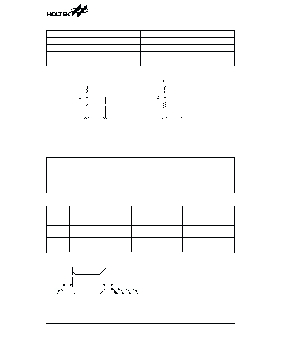
A.C. Test Conditions
Item
Conditions
Input Pulse Level
0V to 3V
Input Rise and Fall Time
5ns
Input and Output Timing Reference Level
1.5V
Output Load
See figures below
Functional Description
Operation truth table
CS
OE
WE
Mode
D0~D7
H
X
X
Standby
High-Z
L
H
H
Output Disable
High-Z
L
L
H
Read
Dout
L
X
L
Write
Din
Data retention characteristics
Ta=
-40°C to 85°C
Symbol
Parameter
Conditions
Min.
Max.
Unit
V
DR
V
DD
for Data Retention
CS
³ V
DD
-0.2V
V
IN
³ V
DD
-0.2V or V
IN
£0.2V
2.0
3.3
V
I
CCDR
Data Retention Current
CS
³ V
DD
-0.2V
V
IN
³ V
DD
-0.2V or V
IN
£0.2V
¾
2
mA
t
CDR
Chip Disable Data Retention Time
See retention timing
0
¾
ns
t
R
Operation Recovery Time
See retention timing
t
RC
*
¾
ns
Low V
DD
data retention timing
HT62L256
Rev. 0.00
4
August 15, 2002
Preliminary
1 0 0 p .
I / O
* I n c l u d i n g s c o p e a n d j i g
+ 1 . 5 V
9 9 0 W
1 . 8 k W
O u t p u t l o a d
O u t p u t l o a d f o r
t
C L Z
, t
O L Z
, t
C H Z
, t
W H Z
a n d t
O W
5 p .
I / O
* I n c l u d i n g s c o p e a n d j i g
+ 1 . 5 V
9 9 0 W
1 . 8 k W
V
D D
C S
t
C D R
3 . 0 V
t
R
3 . 0 V
V
I H
V
I H
V
D D
³ 2 . 0 V
C S ³ V
D D
- 0 . 2 V
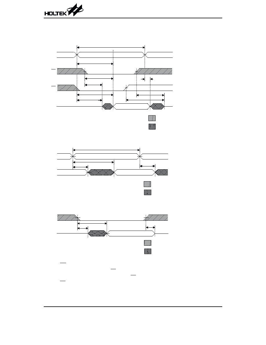
Timing Diagrams
Read cycle 1 output enable controlled (1)
Read cycle 2 address controlled (1, 2, 4)
Read cycle 3 chip select controlled (1, 3, 4)
Note:
1. WE is high for read cycle
2. Device is continuously enabled, CS=V
IL
3. Address is valid prior to or coincident with the CS transition low
4. OE=V
IL
5. Transition is measured at
±500mV from the steady state
HT62L256
Rev. 0.00
5
August 15, 2002
Preliminary
A d d r e s s
D
O U T
t
R C
t
A A
t
O H
t
O H
D o n ' t C a r e
U n u s e d
A d d r e s s
D
O U T
t
A C S
t
C L Z
t
C H Z
D o n ' t C a r e
U n u s e d
A d d r e s s
D
O U T
O E
C S
t
O H
t
R C
t
A A
t
A O E
t
C H Z
t
C L Z
t
O L Z
t
A C S
t
O H Z
D o n ' t C a r e
U n u s e d
Document Outline
- þÿ
- þÿ
- þÿ
- þÿ
- þÿ
- þÿ
- þÿ
- þÿ
- þÿ
- þÿ
- þÿ