 | –≠–ª–µ–∫—Ç—Ä–æ–Ω–Ω—ã–π –∫–æ–º–ø–æ–Ω–µ–Ω—Ç: HT6576 | –°–∫–∞—á–∞—Ç—å:  PDF PDF  ZIP ZIP |

HT6576A
Advanced SCSI CHIP
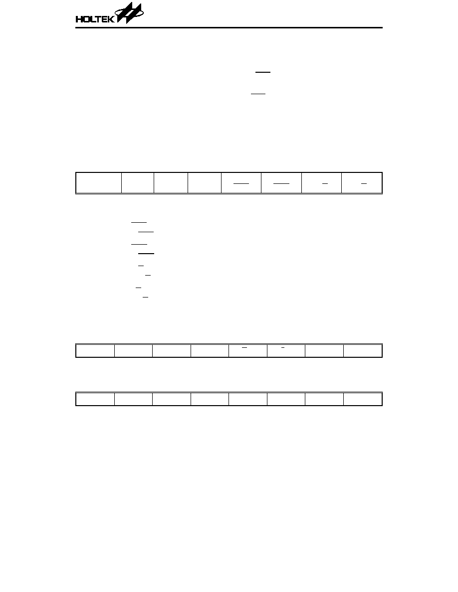
Block Diagram
Features
∑
Support the ANSI X3.131-1986 standard
∑
Asynchronous transfer rate to 5 Mbyte/sec
∑
Support initiator and target mode
∑
0.8um CMOS process
∑
On chip 48mA single-ended drivers and
receivers
∑
Non internal clock needed
∑
44pins PLCC package
1
14th July '97

Pin Diagram
Pin Description
Host Interface Signal
Pin No
Pin Name
I/O
Description
14~16
A0~A2
I
Address Lines
17
CS
I
Chip Select, active low
11
DACK
I
DMA Acknowledge, active low
9
DRQ
O
DMA Request
24~28,
20~22
D0~D7
I/O
Data Lines
10
EOP
I
End of Process, active low
19
IOR
I
I/O Read, active low
18
IOW
I
I/O Write, active low
8
IRQ
O
Interrupt Request
13
READY
O
Ready
7
RESET
I
Reset, active low
HT6576A
2
14th July '97

SCSI Interface Signals
Pin No
Pin Name
I/O
Description
33
ACK
I/O
Acknowledge, active low
6
ATN
I/O
Attention, active low
4
BSY
I/O
Busy, active low
30
C/D
I/O
Control/Data, active low
32
I/O
I/O
Input/Output, active low
29
MSG
I/O
Message, active low
34
REQ
I/O
Request, active low
2
RST
I/O
Reset, active low
37~41,
43, 44, 1
DB0≠DB7
I/O
SCSI Data Bus, active low
35
DBP
I/O
SCSI Parity Bit, active low
5
SEL
I/O
Select, active low
VSS
3, 12, 31, 36, 42
VDD
23
Registers
Address 0
Current SCSI data register(READ ONLY)
DB7
DB6
DB5
DB4
DB3
DB2
DB1
DB0
The SCSI bus parity is checked at the beginning of the read cycle.
Output data register(WRITE ONLY)
DB7
DB6
DB5
DB4
DB3
DB2
DB1
DB0
HT6576A
3
14th July '97

Address 1: Initiator command register
WRITE
7 6 5 4 3 2 1 0
ASSERT
RST
TRI≠STATE RESERVED
ASSERT
ACK
ASSERT
BSY
ASSERT
SEL
ASSERT
ATN
ASSERT
DATA
∑
BIT 7: ASSERT RST
WHEN SET, THE RST SIGNAL IS ASSERTED ON THE SCSI BUS
∑
BIT 6: TRI≠STATE (TEST MODE)
∑
BIT 5: RESERVED (0)
∑
BIT 4: ASSERT ACK
WHEN SET, THE ACK SIGNAL IS ASSERTED ON THE SCSI BUS
∑
BIT 3: ASSERT BSY
WHEN SET, THE BSY SIGNAL IS ASSERTED ON THE SCSI BUS
∑
BIT 2: ASSERT SEL
WHEN SET, THE SEL SIGNAL IS ASSERTED ON THE SCSI BUS
∑
BIT 1: ASSERT ATN
WHEN SET, THE ATN SIGNAL IS ASSERTED ON THE SCSI BUS
∑
BIT 0: ASSERT DATA
WHEN SET, This bit allows the contents of the output data register to be enabled as chip outputs
on SCSI signal DB0≠DB7
READ
7 6 5 4 3 2 1 0
RET
ARBIT
PROGRESS
LOST
ARBIT
ACK
BSY
SEL
ATN
ASSERT
DATA
Address 2: Mode register
READ/WRITE
7 6 5 4 3 2 1 0
LOCK
DMA
TARGET
MODE
ENABLE
PARITY
ENABLE
PARITY
ENABLE
EOP
MONITOR
CHECK
BUSY
DMA
IRQ
MODE
ARBIT
∑
BIT 7: BLOCK MODE DMA
∑
BIT 6: TARGET MODE
When set, the chip operates as an SCSI bus target device.
∑
BIT 5: ENABLE PARITY CHECKING
When set, data received on the SCSI data bus is checked for odd parity.
HT6576A
4
14th July '97
∑
BIT 4: ENABLE PARITY INTERRUPT
When set, this bit causes the IRQ signal to be asserted if a parity error is detected.
∑
BIT 3: ENABLE EOP INTERRUPT
When set, this bit causes the IRQ signal to be asserted if EOP is received from the DMA controller.
∑
BIT 2: MONITOR BUSY
When set, this bit causes the IRQ signa asserted when BSY changes to the inactive state for at
least a bus settle delay.
∑
BIT 1: DMA MODE
∑
BIT 0: Arbitrate
When set, this bit starts the arbitration process.
Address 3: Target command register
7 6 5 4 3 2 1 0
LAST BYTE
X
X
X
ASSERT
REQ
ASSERT
MSG
ASSERT
C/D
ASSERT
I/O
R R/W R/W R/W R/W
∑
BIT 7: LAST BYTE SEND (READ ONLY)
∑
BIT 3: ASSERT REQ
WHEN SET, THE REQ SIGNAL IS ASSERTED ON THE SCSI BUS (IN TARGET MODE)
∑
BIT 2: ASSERT MSG
WHEN SET, THE MSG SIGNAL IS ASSERTED ON THE SCSI BUS (IN TARGET MODE)
∑
BIT 1: ASSERT C/D
WHEN SET, THE C/D SIGNAL IS ASSERTED ON THE SCSI BUS (IN TARGET MODE)
∑
BIT 0: ASSERT I/O
WHEN SET, THE I/O SIGNAL IS ASSERTED ON THE SCSI BUS (IN TAGRTE MODE)
Address 4: Current SCSI Bus Register
READ
7 6 5 4 3 2 1 0
RST
BSY
REQ
MSG
C/D
I/O
SEL
DBP
WRITE ≠SELECT ENABLE REGISTER
7 6 5 4 3 2 1 0
SID7
SID6
SID5
SID4
SID3
SID2
SID1
SID0
HT6576A
5
14th July '97