 | ÐлекÑÑоннÑй компоненÑ: HT6751B | СкаÑаÑÑ:  PDF PDF  ZIP ZIP |
Äîêóìåíòàöèÿ è îïèñàíèÿ www.docs.chipfind.ru
HT6751A/B
Camera Motor Driver (1.5 Channel)
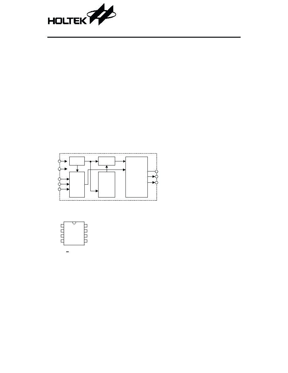
Block Diagram
Pin Assignment
1
August 7, 2000
Features
·
Operating voltage: 2.0V~6.0V
·
Operating current < 2mA at 3.0V, No load
·
Standby current I
VDD
< 2mA, no load
·
Separate logic power supply and motor
power supply
·
Built-in thermal shutdown circuit
·
Built-in H bridge control circuit
·
Built-in spark killer diode
·
Provides strong ESD (min. of 4KV) per pin
·
8-pin SOP package
Applications
·
Camera motor driver
·
Toy motor driver
General Description
The IC can control H Bridge circuit for motor
driving. It provides Spark Killer Diode/Ther-
mal Shutdown function/Forward function/Re-
verse function/Brake function/Stop function for
motor driver application. It is designed by LSI
high technology with low power process.
R C
O s c i l l a t o r
C h a r g e
P u m p
I n p u t
C o n t r o l
T h e r m a l
S h u t d o w n
C i r c u i t
H B r i d g e
M o t o r D r i v e
C i r c u i t
I N 1
I N 2
I N 3
V M
O U T 1
O U T 2
V D D
V S S
1
2
3
4
8
7
6
5
H T 6 7 5 1 A / B
8 S O P
V M
O U T 1
I N 3
V S S
O U T 2
I N 2
V D D
I N 1
Pin Description
Pin No.
Pin Name
I/O
Description
1
VM
P
Power of motor driving circuit
2
OUT1
O
Connect to motor terminal
3
IN3
I
Input signal
4
VSS
¾
Negative power supply, ground
5
IN1
I
Input signal
6
VDD
¾
Positive power supply
7
IN2
I
Input signal
8
OUT2
O
Connect to motor terminal
Absolute Maximum Ratings
Supply Voltage.......................V
DD
-0.3V to 7.0V
Storage Temperature.................-40°C to 125°C
Voltage to Input Terminal .....-0.3V to V
DD
+0.3
Operating Temperature ..............-20°C to 85°C
Junction Temperature ..............................150°C
Note: These are stress ratings only. Stresses exceeding the range specified under ²Absolute Maxi-
mum Ratings² may cause substantial damage to the device. Functional operation of this de-
vice at other conditions beyond those listed in the specification is not implied and prolonged
exposure to extreme conditions may affect device reliability.
Electrical Characteristics
Ta=25°C
Symbol
Parameter
Test Conditions
Min. Typ.
Max.
Unit
V
DD
Conditions
V
DD
Operating Voltage 1
¾
¾
2.0
¾
6.0
V
VM
Operating Voltage 2
¾ Motor loading
1.8
¾
6.0
V
I
VM
V
M
Current
5V Standby mode with
internal pump
¾
¾
10
mA
I
OPR
Operating Current
5V No load @ V
DD
=5V
¾
¾
2
mA
I
VDD
Standby Current
5V Standby mode
¾
1
2
mA
I
IL
Input Leakage Current
5V 0<Vin<V
DD
-1.0
¾
1.0
mA
V
IL
Input Low Voltage
5V
¾
-0.3
0.3V
DD
V
V
IH
Input High Voltage
5V
¾
0.6V
DD
¾ V
DD
+0.3
V
R
ON
H Bridge On Resistance
3V (up_NMOS+down_
NMOS) at 3V
¾
¾
0.4
W
HT6751A/B
2
August 7, 2000
Symbol
Parameter
Test Conditions
Min. Typ.
Max.
Unit
V
DD
Conditions
t
CP_ON
Charge Pump Turn On
Time
5V V
DD
=VM=5V,
Ivm=0.5A
¾
¾
2
ms
t
CP_OFF
Charge Pump Turn Off
Time
5V V
DD
=VM=5V,
Ivm=0.5A
¾
¾
1
ms
t
H_ON
H Bridge Turn On Time
5V V
DD
=VM=5V,
Ivm=0.5A
¾
¾
10
ms
t
H_OFF
H Bridge Turn Off Time
5V V
DD
=VM=5V,
Ivm=0.5A
¾
¾
5
ms
Functional Description
HT6751A/B
3
August 7, 2000
·
In HT6751A function
IN1
IN2
IN3
Function
MOS On
MOS Off
0
1
1
Motor1 forward
P1/N2
P2/N1
1
0
1
Motor1 reverse
P2/N1
P1/N2
0
0
1
Motor1 brake
N1/N2
P1/P2
1
1
1
Standby mode
¾
P1/P2/N1/N2
0
1
0
Motor2 forward
P2/(N3)
N2/(P3)
1
0
0
Motor2 reverse
N2/(P3)
P2/(N3)
0
0
0
Motor2 brake
N2/(N3)
P2/(P3)
·
In HT6751B function
IN1
IN2
IN3
Function
MOS On
Mos Off
1
0
0
Motor1 forward
P1/N2
P2/N1
0
1
0
Motor1 reverse
P2/N1
P1/N2
1
1
0
Motor1 brake
N1/N2
P1/P2
0
0
0
Standby mode
¾
P1/P2/N1/N2
1
0
1
Motor2 forward
P2/(N3)
N2/(P3)
0
1
1
Motor2 reverse
N2/(P3)
P2/(N3)
1
1
1
Motor2 brake
N2/(N3)
P2/(P3)
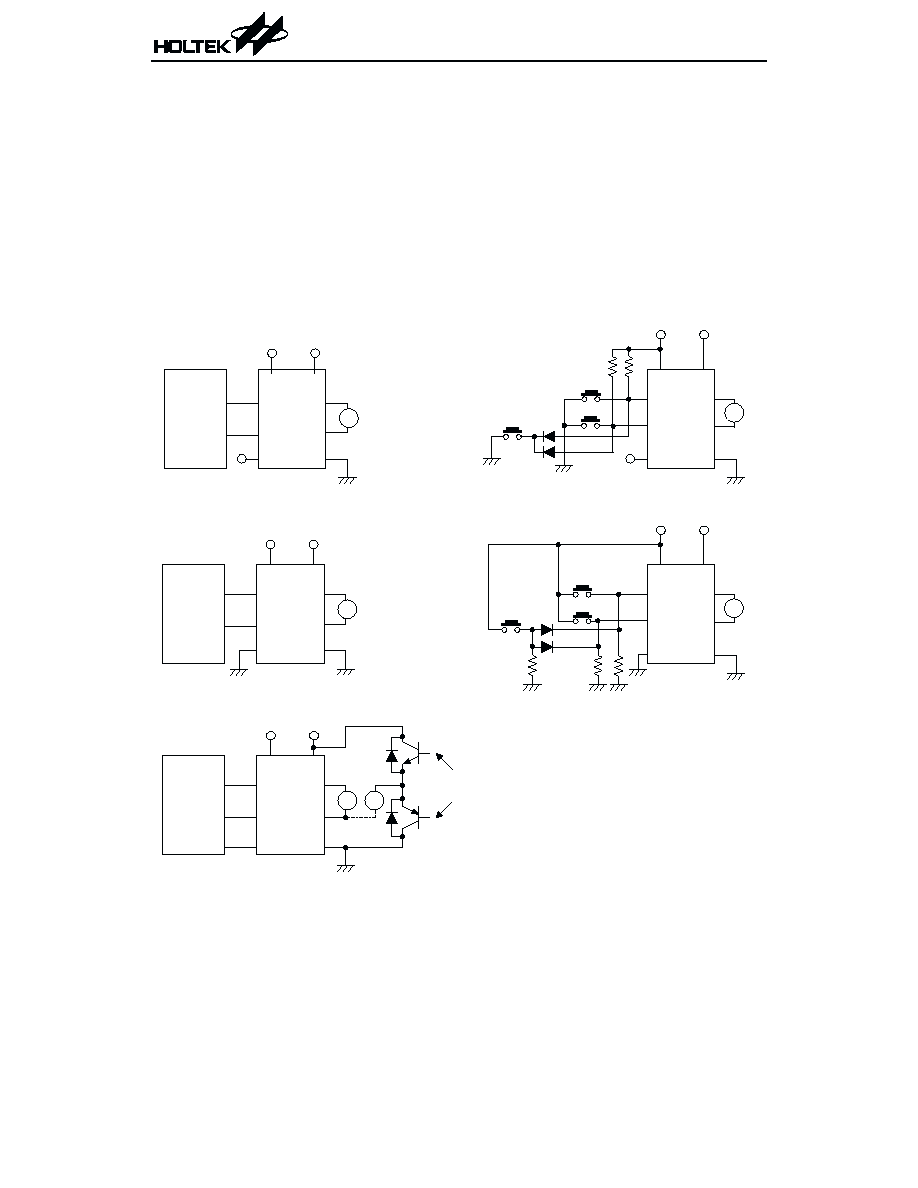
Application Circuits
HT6751A/B
4
August 7, 2000
¨
In normal state and standby mode
Charge pump circuit is in off state
Oscillator circuit is in off state
Standby current is below 2mA
For HT6751A, the oscillator circuit and
charge pump circuit is on until IN1 or IN2
or IN3 is low input
For HT6751B, the oscillator circuit and
charge pump circuit is on until IN1 or IN2
or IN3 is high input
¨
The system enters thermal shutdown mode
(current is limited below 500mA) when the
temperature of the internal sensor is
greater than Junction Temperature and
then release this mode until the tempera-
ture of the internal sensor below (Junction
Temperatue >150°C). The system can ac-
cept IN1/IN2/IN3 signal when in thermal
shutdown mode.
I N 1
I N 2
I N 3
O U T 1
O U T 2
V S S
V D D
1 . 5 C h a n n e l
f o r
m C / A S I C
M 1
V M
M 2
P 3
O U T 3
V
D D
N 3
E x t e r n a l
H T 6 7 5 1 A / B
V
M
I N 1
I N 2
I N 3
O U T 1
O U T 2
V S S
V D D
1 C h a n n e l
f o r
m C / A S I C
M 1
V M
H T 6 7 5 1 A
V
D D
V
M
V
D D
I N 1
I N 2
I N 3
O U T 1
O U T 2
V S S
V D D
1 C h a n n e l
f o r
m C / A S I C
M 1
V M
H T 6 7 5 1 B
V
D D
V
M
I N 1
I N 2
I N 3
O U T 1
O U T 2
V S S
V D D
M
V M
H T 6 7 5 1 A
V
D D
V
M
V
D D
F o r w a r d
R e v e r s e
B r a k e
I N 1
I N 2
I N 3
V S S
V D D
V M
V
D D
V
M
F o r w a r d
R e v e r s e
B r a k e
H T 6 7 5 1 B
O U T 1
O U T 2
M
HT6751A/B
5
August 7, 2000
Copyright ã 2000 by HOLTEK SEMICONDUCTOR INC.
The information appearing in this Data Sheet is believed to be accurate at the time of publication. However, Holtek
assumes no responsibility arising from the use of the specifications described. The applications mentioned herein are
used solely for the purpose of illustration and Holtek makes no warranty or representation that such applications
will be suitable without further modification, nor recommends the use of its products for application that may pres-
ent a risk to human life due to malfunction or otherwise. Holtek reserves the right to alter its products without prior
notification. For the most up-to-date information, please visit our web site at http://www.holtek.com.tw.
Holtek Semiconductor Inc. (Headquarters)
No.3 Creation Rd. II, Science-based Industrial Park, Hsinchu, Taiwan, R.O.C.
Tel: 886-3-563-1999
Fax: 886-3-563-1189
Holtek Semiconductor Inc. (Taipei Office)
5F, No.576, Sec.7 Chung Hsiao E. Rd., Taipei, Taiwan, R.O.C.
Tel: 886-2-2782-9635
Fax: 886-2-2782-9636
Fax: 886-2-2782-7128 (International sales hotline)
Holtek Semiconductor (Hong Kong) Ltd.
RM.711, Tower 2, Cheung Sha Wan Plaza, 833 Cheung Sha Wan Rd., Kowloon, Hong Kong
Tel: 852-2-745-8288
Fax: 852-2-742-8657
Document Outline
- þÿ
- þÿ
- þÿ
- þÿ
- þÿ
- þÿ
- þÿ
- þÿ
- þÿ
- þÿ