 | ÐлекÑÑоннÑй компоненÑ: HT6P20 | СкаÑаÑÑ:  PDF PDF  ZIP ZIP |
Äîêóìåíòàöèÿ è îïèñàíèÿ www.docs.chipfind.ru
HT6P20
2
24
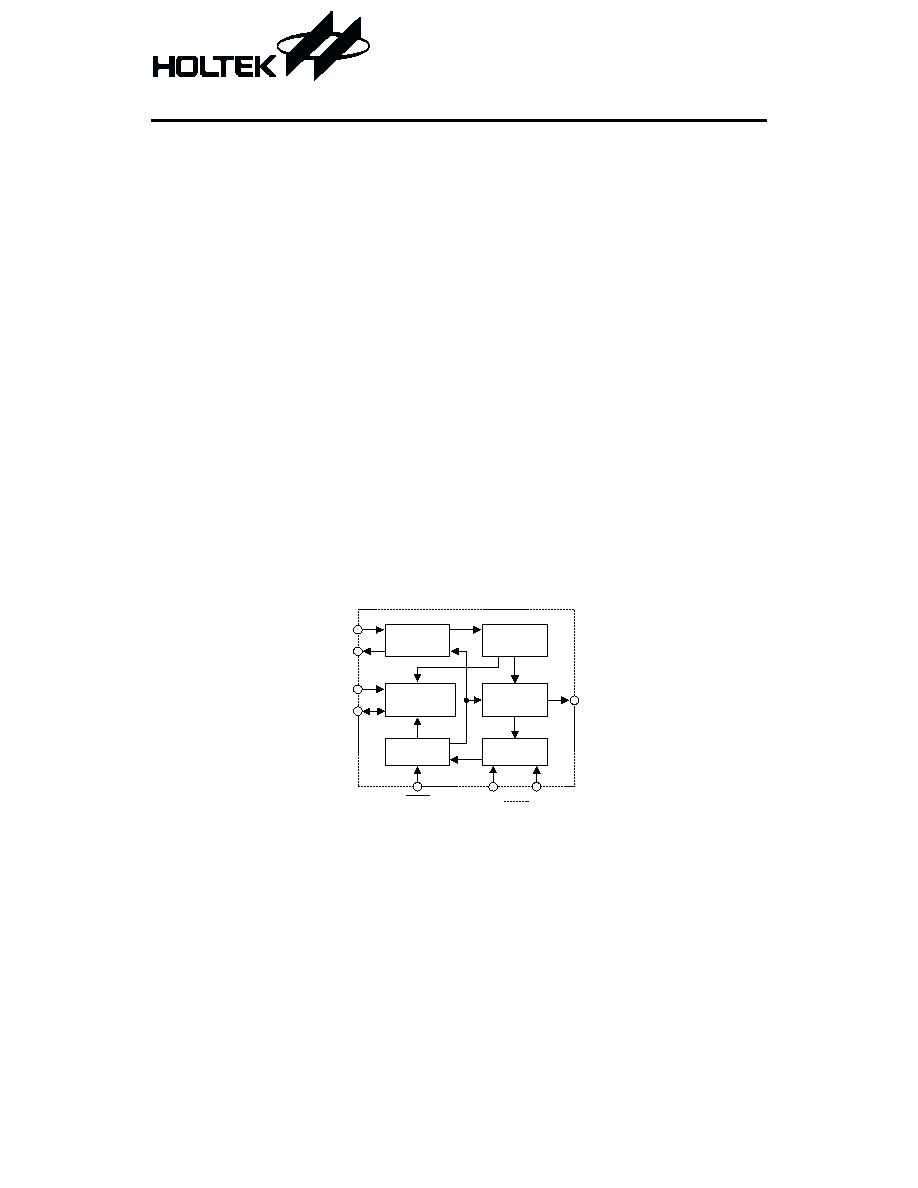
OTP Encoder
Block Diagram
Note: Address/Data numbers are available in various combinations, refer to the functional descrip
tion.
1
May 2, 2000
Features
·
Operating voltage: 2V~12V
·
Low power consumption
·
Built-in oscillator needs only 5% resistor
·
0/2/4/8 data selectable
·
2
24
maximum address and data codes
·
Easy interface with an RF or IR medium
·
One time programmable process
·
Data active: D0~D7
·
Minimal external components
·
HT6P20/A/B: 8-pin DIP/NSOP package
HT6P20/D: 16-pin DIP/NSOP package
General Description
The HT6P20 is a CMOS LSI encoder designed
for remote control system applications. It en-
codes 24 bits of information and then serially
transmits it via the DOUT pin upon receipt of
transmission enable (DATA pins: D0~D7) sig-
nals. The combination of address and data bits
of the HT6P20 is designed using one time pro-
grammable process. In addition, the chip offers
various packaging for flexible combination of
programmable address/data so as to meet vari-
ous applications. Its programmable ad-
dress/data is transmitted together with the
anti-code bits via RF or infrared transmission
medium upon receipt of a trigger signal.
Applications
·
Burglar alarm system
·
Smoke and fire alarm system
·
Garage door controllers
·
Car door controllers
·
Security system
·
Cordless telephones
·
Other remote control systems
O s c i l l a t o r
P r o g r a m m i n g
C i r c u i t
C o n t r o l U n i t
A d d r e s s
C o u n t e r
D a t a L a t c h
V P P
S I O
M i x e r &
D r i v e r
D O U T
O S C 1
O S C 2
P G M
D 0
D 7
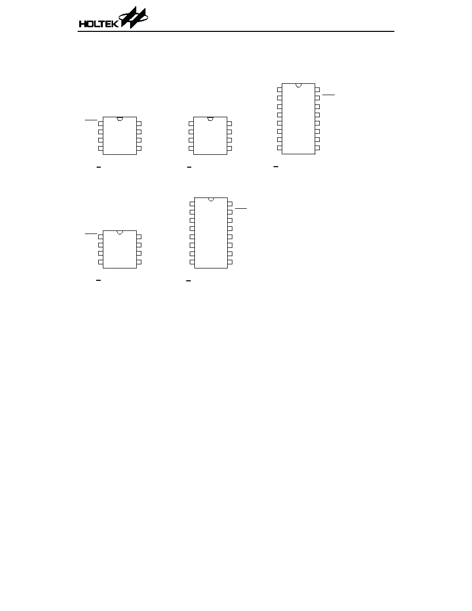
Pin Assignment
Note: The customer code and control code have been programmed into HT6P20A/B/D by Holtek¢s
factory process.
The blank device HT6P20 is not programmed, it can be programmed by Holtek¢s programming
kit.
Warning: The 8-pin blank device only allows programming as HT6P20A type.
The 16-pin blank device allows programming as one of HT6P20/D type. After program-
ming the HT6P20 pin name are the same as one of HT6P20D, which is determined by the
kit programming procedure.
Pin name ²NC² stands for no connection (floating).
HT6P20
2
May 2, 2000
1
2
3
4
8
7
6
5
S I O
V P P
V D D
D O U T
P G M
V S S
O S C 2
O S C 1
2 4 - A d d r e s s
0 - D a t a
2 0 - A d d r e s s
4 - D a t a
1 6
1 5
1 4
1 3
1 2
1 1
1 0
9
1
2
3
4
5
6
7
8
D 0
P G M
S I O
V P P
V D D
D O U T
O S C 1
O S C 2
D 1
D 2
D 3
V S S
N C
N C
N C
N C
1
2
3
4
8
7
6
5
N C
V D D
D O U T
O S C 1
D 0
D 1
V S S
O S C 2
2 2 - A d d r e s s
2 - D a t a
B l a n k d e v i c e
B l a n k d e v i c e
1 6
1 5
1 4
1 3
1 2
1 1
1 0
9
1
2
3
4
5
6
7
8
D 0
P G M
S I O
V P P
V D D
D O U T
O S C 1
O S C 2
D 1
D 2 / N C
D 3 / N C
V S S
D 4 / N C
D 5 / N C
D 6 / N C
D 7 / N C
H T 6 P 2 0 A
8 D I P / N S O P
H T 6 P 2 0 B
8 D I P / N S O P
H T 6 P 2 0 D
1 6 D I P / N S O P
H T 6 P 2 0
1 6 D I P / N S O P
1
2
3
4
8
7
6
5
S I O
V P P
V D D
D O U T
P G M
V S S
O S C 2
O S C 1
H T 6 P 2 0
8 D I P / N S O P
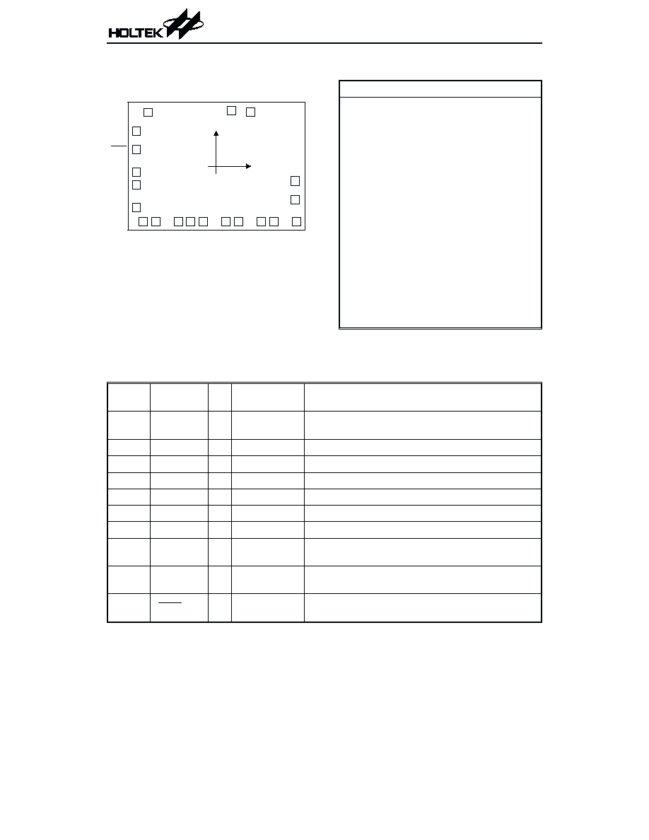
Pad Assignment
Pad Coordinates
Unit: mm
Pad No.
X
Y
1
-956.50
762.75
2
-1123.00
498.75
3
-1123.00
236.25
4
-1123.00
-86.25
5
-1123.00
-261.25
6
-1123.00
-583.75
7
-1027.50
-776.75
8
-852.50
-776.75
9
-530.00
-776.75
10
-355.00
-776.75
11
-180.00
-776.75
12
142.50
-776.75
13
317.50
-776.75
14
640.00
-776.75
15
815.00
-776.75
16
1137.50
-776.75
17
1118.00
-466.75
18
1118.00
-205.75
19
489.00
772.05
20
223.50
789.75
Pin Description
HT6P20D
Pin No. Pin Name I/O
Internal
Connection
Description
16
1~3
D0~D3
I
CMOS IN
Pull-high
Data input and transmission enable (active low)
They can be externally set to VSS or left open.
4
VSS
¾
¾
Negative power supply, ground
5~8
NC
¾
¾
No connection
9
OSC2
O OSCILLATOR Oscillator output pin
10
OSC1
I
OSCILLATOR Oscillator input pin
11
DOUT
O
CMOS OUT
Data serial transmission output
12
VDD
¾
¾
Positive power supply
13
VPP
I
¾
Programming power supply, V
DD
for normal opera-
tion
14
SIO
I/O
CMOS
IN/OUT
Programming address/control code input and mode
code output for mode verification
15
PGM
I
CMOS IN
Pull-high
Program mode control pin, active low
HT6P20
3
May 2, 2000
1
2
3
4
5
6
7 8
9 1 0 1 1
1 2 1 3
1 4 1 5
1 6
1 7
1 8
1 9
2 0
( 0 , 0 )
S I O
P G M
D 0
D 1
D2
D3
VS
S
D4
D5
D6
D 7
O S C 2
O S C 1
DO
UT
VD
D
VP
P
NC
N C
NC
NC
Chip size: 2590 ´ 2010 (mm)
2
* The IC substrate should be connected to VSS in
the PCB layout artwork.
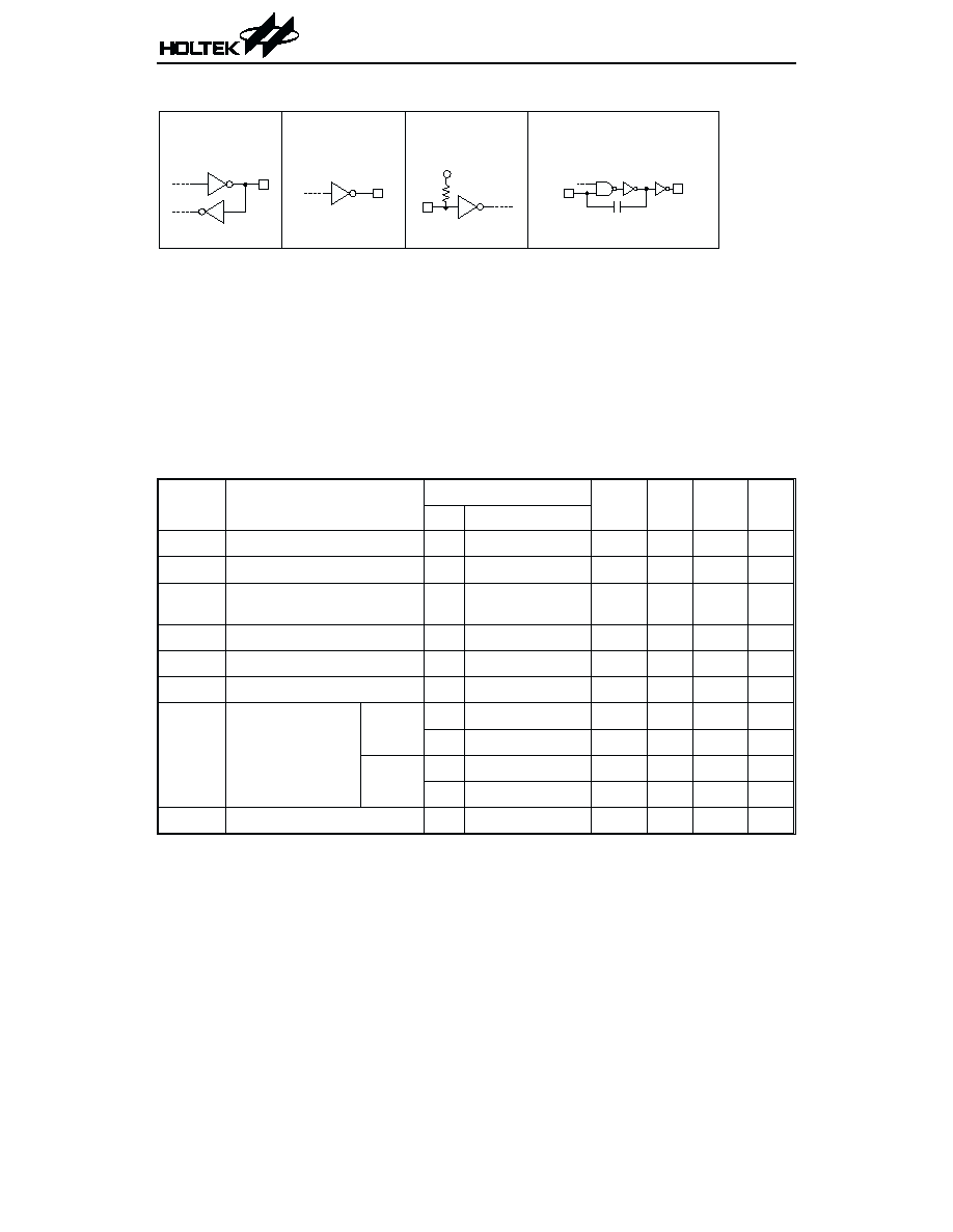
Approximate internal connection circuits
Absolute Maximum Ratings
Supply Voltage ..............................-0.3V to 12V
Storage Temperature.................-50°C to 125°C
Input Voltage.................V
SS
-0.3V to V
DD
+0.3V
Operating Temperature ..............-20°C to 75°C
Note: These are stress ratings only. Stresses exceeding the range specified under ²Absolute Maxi-
mum Ratings² may cause substantial damage to the device. Functional operation of this de-
vice at other conditions beyond those listed in the specification is not implied and prolonged
exposure to extreme conditions may affect device reliability.
Electrical Characteristics
Ta=25°C
Symbol
Parameter
Test Conditions
Min.
Typ. Max. Unit
V
DD
Conditions
V
DD
Operating Voltage
¾
¾
2
¾
12
V
I
STB
Standby Current
12V
Oscillator stops
¾
1
2
mA
I
DD
Operating Current
12V
No load
f
OSC
=3kHz
¾
200
400
mA
V
IH
²H² Input Voltage
¾
¾
0.8V
DD
¾
V
DD
V
V
IL
²L² Input Voltage
¾
¾
0
¾
0.2V
DD
V
R
PH
D0~D7 Pull-high Resistance 12V
¾
¾
150
300
kW
I
DOUT
Output Current
Source
5V
0.9V
DD
-2
-5
¾
mA
12V
0.9V
DD
-6.5
-15
¾
mA
Sink
5V
0.1V
DD
2
5
¾
mA
12V
0.1V
DD
6
15
¾
mA
f
OSC
Oscillator Frequency
12V
R
OSC
=1.4MW
¾
3
¾
kHz
HT6P20
4
May 2, 2000
C M O S I N / O U T
C M O S I N
P u l l - h i g h
O S C I L L A T O R
O S C 1
O S C 2
C M O S O U T
V
D D
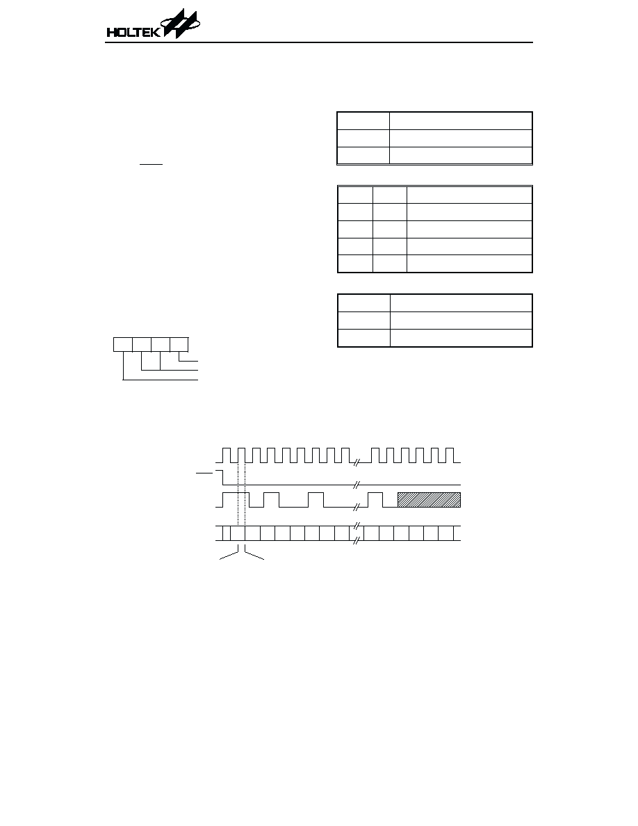
Programming timing of the HT6P20D (B0~B3=1010)
HT6P20
5
May 2, 2000
Functional Description
Programming
The HT6P20 is a one time programmable encod-
ing integrated circuit. The programmable codes
consist of 4-bit control codes and 24-bit address
codes. Before using the device, first program the
internal 4 control bits and 24 address bits. Then,
to program the address and control codes, con-
nect the PGM pin to VSS, allowing the SIO pin to
receive control and address codes from the con-
tinuously transmitting programming kit. The
control codes (B0~B3) and address timing are re-
spectively shown on the Table and the Figure for
Programming Timing. In the programming pro-
cess, the mode bit (B0) has to be programmed
first. The 0/2/4/8 data number is selected by the
address along with the data format bits (B1,B2).
The HT6P20, in addition, provides a polarity bit
(B3) to select the polarity of the output data.
Various packages of the HT6P20 offer program-
mable combinations of address/data to meet
various application needs.
Table 1: Control code
·
Mode control (B0)
B0
Function
0
Not programmed
1
Programmed
·
Address and data format (B1,B2)
B2
B1
Code Format
0
0
A0~A23
0
1
A0~A21 + D1~D0
1
0
A0~A19 + D3~D0
1
1
A0~A15 + D7~D0
·
Polarity control (B3)
B3
Data Output Polarity
0
Negative polarity
1
Positive polarity
The HT6P20A/D can be programmed by the
SIO pins. The HT6P20B, on the other hand, is
programmed for 2-data and positive polarity
application.
B 0
B 1 B 2
B 3
P o l a r i t y c o n t r o l
A d d r e s s a n d d a t a f o r m a t
M o d e c o n t r o l
O S C 2
( 3 k H z )
P G M
S I O
B 0
B 1 B 2
B 3
A 0
A 1 A 2
A 3
A 18 A 19 A 2 0 A 2 1A 2 2 A 2 3
P r o g r a m m i n g
P r o g r a m m i n g
b i t
N o t e : ( 1 ) B 0 ~ B 3 a r e c o n t r o l c o d e s
( 2 ) A 0 ~ A 2 3 a r e a d d r e s s c o d e s
( 3 ) A 2 0 ~ A 2 3 s t a n d s f o r d o n ' t c a r e f o r t h e H T 6 P 2 0 D
1
0
1
0
0
1
0
0
1
0
X
X
X
X
( 5 ) 0 : " L o w " ; 1 : " H i g h " ; X : D o n ' t c a r e
1
( 4 ) S I O m u s t b e s e t t o " H i g h " d u r i n g C a n d B 0 p e r i o d s
C
Programming timing for the HT6P20D
Document Outline
- þÿ
- þÿ
- þÿ
- þÿ
- þÿ
- þÿ
- þÿ
- þÿ
- þÿ
- þÿ
- þÿ
- þÿ