 | ÐлекÑÑоннÑй компоненÑ: HT6P20E | СкаÑаÑÑ:  PDF PDF  ZIP ZIP |
HT6P20/6P20A/6P20B/6P20D - 2^24 OTP Encoder
HT6P20 Series
2
24
OTP Encoder
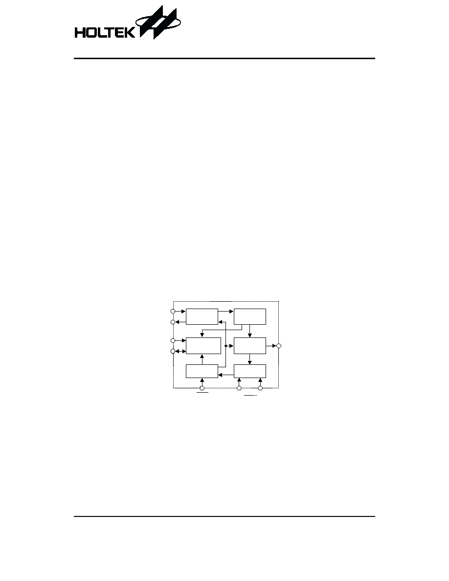
Block Diagram
Note: Address/Data numbers are available in various combinations, refer to the functional description.
Rev. 1.30
1
April 10, 2003
Features
·
Operating voltage: 2V~12V
·
Low power consumption
·
Built-in oscillator needs only 5% resistor
·
0/2/4/8 data selectable
·
2
24
maximum address and data codes
·
Easy interface with an RF or IR medium
·
One time programmable process
·
Data active: D0~D7
·
Minimal external components
·
HT6P20/A/B: 8-pin DIP/SOP package
HT6P20/D: 16-pin DIP/NSOP package
General Description
The HT6P20 is a CMOS LSI encoder designed for re-
mote control system applications. It encodes 24 bits of
information and then serially transmits it via the DOUT
pin upon receipt of transmission enable (DATA pins:
D0~D7) signals. The combination of address and data
bits of the HT6P20 is designed using one time program-
mable process. In addition, the chip offers various pack-
aging for flexible combination of programmable
address/data so as to meet various applications. Its pro-
grammable address/data is transmitted together with
the anti-code bits via RF or infrared transmission me-
dium upon receipt of a trigger signal.
Applications
·
Burglar alarm system
·
Smoke and fire alarm system
·
Garage door controllers
·
Car door controllers
·
Security system
·
Cordless telephones
·
Other remote control systems
O s c i l l a t o r
P r o g r a m m i n g
C i r c u i t
C o n t r o l U n i t
A d d r e s s
C o u n t e r
D a t a L a t c h
V P P
S I O
M i x e r &
D r i v e r
D O U T
O S C 1
O S C 2
P G M
D 0
D 7
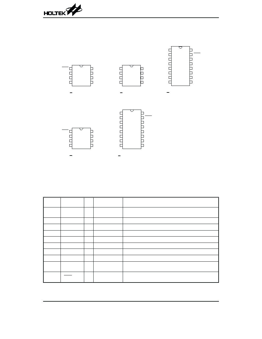
Pin Assignment
Note:
The customer code and control code have been programmed into HT6P20A/B/D by Holtek
¢s factory process.
The 8-pin blank device only allows programming as HT6P20A type and the 16-pin blank device allows pro-
gramming as HT6P20D type.
Pin Description
HT6P20D
Pin No.
Pin Name
I/O
Internal
Connection
Description
16
1~3
D0~D3
I
CMOS IN
Pull-high
Data input and transmission enable (active low)
They can be externally set to VSS or left open.
4
VSS
¾
¾
Negative power supply, ground
5~8
NC
¾
¾
No connection
9
OSC2
O
OSCILLATOR
Oscillator output pin
10
OSC1
I
OSCILLATOR
Oscillator input pin
11
DOUT
O
CMOS OUT
Data serial transmission output
12
VDD
¾
¾
Positive power supply
13
VPP
I
¾
Programming power supply, V
DD
for normal operation
14
SIO
I/O
CMOS
IN/OUT
Programming address/control code input and mode code out-
put for mode verification
15
PGM
I
CMOS IN
Pull-high
Program mode control pin, active low
HT6P20 Series
Rev. 1.30
2
April 10, 2003
1
2
3
4
8
7
6
5
S I O
V P P
V D D
D O U T
P G M
V S S
O S C 2
O S C 1
2 4 - A d d r e s s
0 - D a t a
2 0 - A d d r e s s
4 - D a t a
1 6
1 5
1 4
1 3
1 2
1 1
1 0
9
1
2
3
4
5
6
7
8
D 0
P G M
S I O
V P P
V D D
D O U T
O S C 1
O S C 2
D 1
D 2
D 3
V S S
N C
N C
N C
N C
1
2
3
4
8
7
6
5
N C
V D D
D O U T
O S C 1
D 0
D 1
V S S
O S C 2
2 2 - A d d r e s s
2 - D a t a
B l a n k d e v i c e
B l a n k d e v i c e
1 6
1 5
1 4
1 3
1 2
1 1
1 0
9
1
2
3
4
5
6
7
8
D 0
P G M
S I O
V P P
V D D
D O U T
O S C 1
O S C 2
D 1
D 2 / N C
D 3 / N C
V S S
D 4 / N C
D 5 / N C
D 6 / N C
D 7 / N C
H T 6 P 2 0 A
8 D I P / S O P
H T 6 P 2 0 B
8 D I P / S O P
H T 6 P 2 0 D
1 6 D I P / N S O P
H T 6 P 2 0
1 6 D I P / N S O P
1
2
3
4
8
7
6
5
S I O
V P P
V D D
D O U T
P G M
V S S
O S C 2
O S C 1
H T 6 P 2 0
8 D I P / S O P
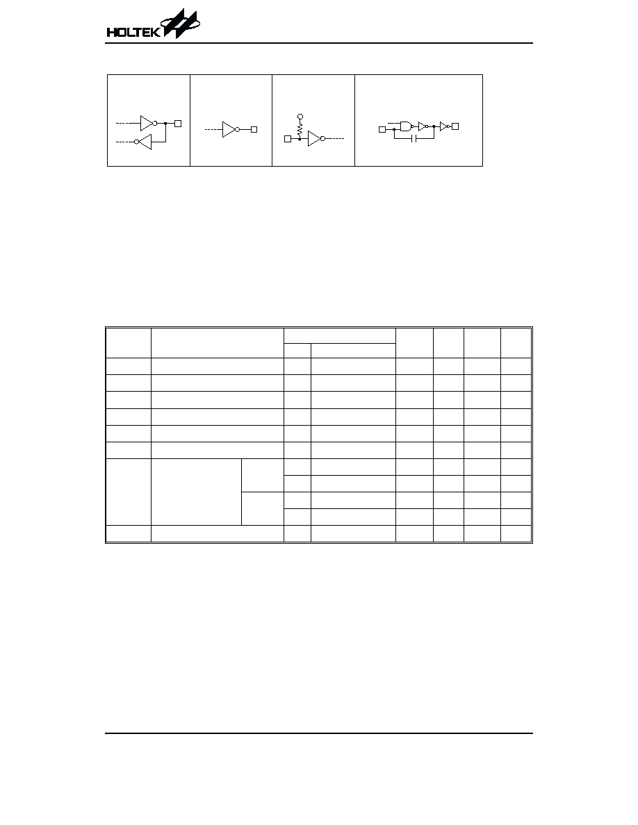
Approximate internal connection circuits
Absolute Maximum Ratings
Supply Voltage .........................................
-0.3V to 12V
Storage Temperature ............................
-50°C to 125°C
Input Voltage..............................V
SS
-0.3V to V
DD
+0.3V
Operating Temperature...........................
-20°C to 75°C
Note: These are stress ratings only. Stresses exceeding the range specified under
²Absolute Maximum Ratings² may
cause substantial damage to the device. Functional operation of this device at other conditions beyond those
listed in the specification is not implied and prolonged exposure to extreme conditions may affect device reliabil-
ity.
Electrical Characteristics
Ta=25
°C
Symbol
Parameter
Test Conditions
Min.
Typ.
Max.
Unit
V
DD
Conditions
V
DD
Operating Voltage
¾
¾
2
¾
12
V
I
STB
Standby Current
12V
Oscillator stops
¾
1
2
mA
I
DD
Operating Current
12V
No load, f
OSC
=3kHz
¾
200
400
mA
V
IH
²H² Input Voltage
¾
¾
0.8V
DD
¾
V
DD
V
V
IL
²L² Input Voltage
¾
¾
0
¾
0.2V
DD
V
R
PH
D0~D7 Pull-high Resistance
12V
¾
¾
150
300
k
W
I
DOUT
Output Current
Source
5V
0.9V
DD
-2
-5
¾
mA
12V
0.9V
DD
-6.5
-15
¾
mA
Sink
5V
0.1V
DD
2
5
¾
mA
12V
0.1V
DD
6
15
¾
mA
f
OSC
Oscillator Frequency
12V
R
OSC
=1.4M
W
¾
3
¾
kHz
HT6P20 Series
Rev. 1.30
3
April 10, 2003
C M O S I N / O U T
C M O S I N
P u l l - h i g h
O S C I L L A T O R
O S C 1
O S C 2
C M O S O U T
V
D D
Programming Timing of the HT6P20D (B0~B3=1010)
HT6P20 Series
Rev. 1.30
4
April 10, 2003
Functional Description
Programming
The HT6P20 is a one time programmable encoding inte-
grated circuit. The programmable codes consist of 4-bit
control codes and 24-bit address codes. Before using the
device, first program the internal 4 control bits and 24 ad-
dress bits. Then, to program the address and control
codes, connect the PGM pin to VSS, allowing the SIO pin
to receive control and address codes from the continu-
ously transmitting programming kit. The control codes
(B0~B3) and address timing are respectively shown on
the Table and the Figure for Programming Timing. In the
programming process, the mode bit (B0) has to be pro-
grammed first. The 0/2/4/8 data number is selected by the
address along with the data format bits (B1,B2). The
HT6P20, in addition, provides a polarity bit (B3) to select
the polarity of the output data.
Various packages of the HT6P20 offer programmable
combinations of address/data to meet various applica-
tion needs.
Table 1: Control Code
·
Mode control (B0)
B0
Function
0
Not programmed
1
Programmed
·
Address and data format (B1,B2)
B2
B1
Code Format
0
0
A0~A23
0
1
A0~A21 + D1~D0
1
0
A0~A19 + D3~D0
1
1
A0~A15 + D7~D0
·
Polarity control (B3)
B3
Data Output Polarity
0
Negative polarity
1
Positive polarity
The HT6P20A/D can be programmed by the SIO pins.
The HT6P20B, on the other hand, is programmed for
2-data and positive polarity application.
O S C 2
( 3 k H z )
P G M
S I O
B 0
B 1
B 2
B 3
A 0
A 1
A 2
A 3
A 1 8 A 1 9 A 2 0 A 2 1 A 2 2 A 2 3
P r o g r a m m i n g
P r o g r a m m i n g
b i t
N o t e : ( 1 ) B 0 ~ B 3 a r e c o n t r o l c o d e s
( 2 ) A 0 ~ A 2 3 a r e a d d r e s s c o d e s
( 3 ) A 2 0 ~ A 2 3 s t a n d s f o r d o n ' t c a r e f o r t h e H T 6 P 2 0 D
1
0
1
0
0
1
0
0
1
0
X
X
X
X
( 5 ) 0 : " L o w " ; 1 : " H i g h " ; X : D o n ' t c a r e
1
( 4 ) S I O m u s t b e s e t t o " H i g h " d u r i n g C a n d B 0 p e r i o d s
C
Programming timing for the HT6P20D
B 0
B 1
B 2
B 3
P o l a r i t y c o n t r o l
A d d r e s s a n d d a t a f o r m a t
M o d e c o n t r o l
Normal Operation
The HT6P20 encodes and transmits address/data to a decoder upon receipt of a trigger signal. The address codes of
the HT6P20A are always transmitted as long as power (VDD) is supplied. The transmission function of the HT6P20B/D
is enabled by the D0~D7 pins (active low). The following is the transmission timing of the HT6P20:
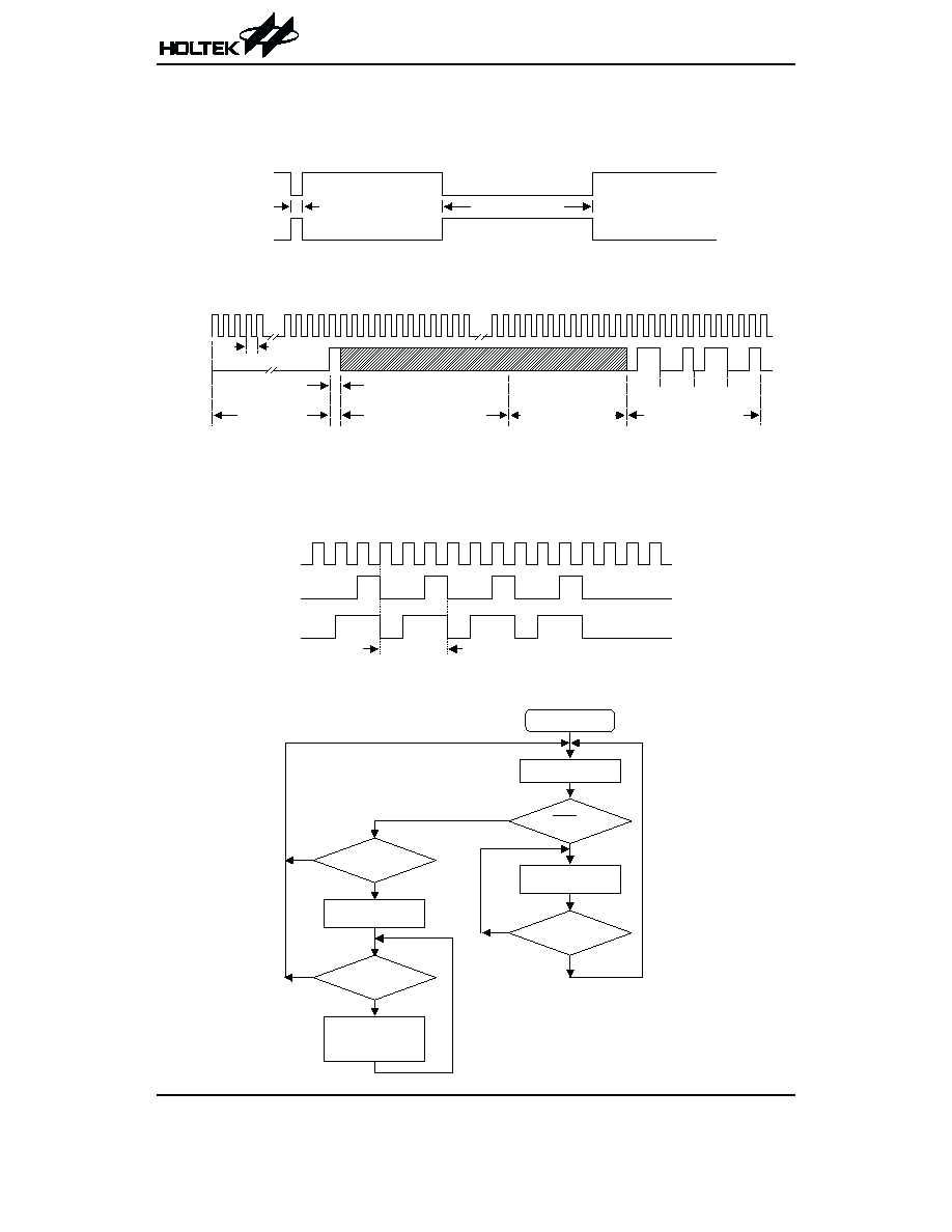
A complete code word of the HT6P20D consists of 3 periods as shown below.
The HT6P20A/B/D detects the logic state of the internal programmed address and the external data pins, and then trans-
mits the detected information during the code period. Each address/data bit can be set to one of the following two logic
states:
Flowchart
HT6P20 Series
Rev. 1.30
5
April 10, 2003
a n t i - c o d e p e r i o d
( 4 b i t s )
p i l o t p e r i o d
( 2 3 c l o c k s )
a d d r e s s c o d e p e r i o d
d a t a c o d e p e r i o d
1 / 3 b i t
( A 0 ~ A 1 9 , 6 0 c l o c k s )
( D 3 ~ D 0 , 1 2 c l o c k s )
0
0
1
1
f o s c
D O U T
1 c l o c k
A complete code word for the HT6P20D
E n c o d e r
D O U T
< 1 w o r d
D 0 ~ D 7
> 1 w o r d
Transmission timing
" O n e "
" Z e r o "
f o s c
A d d r e s s /
D a t a b i t
S t a n d b y m o d e
T r a n s m i s s i o n
e n a b l e d ?
N o
N o
Y e s
Y e s
A d d r e s s / d a t a w o r d s
t r a n s m i t t e d
T r a n s m i s s i o n
s t i l l e n a b l e d
A d d r e s s / d a t a w o r d s
t r a n s m i t t e d
c o n t i n u o u s l y
P o w e r o n
P G M = 0 ?
N o
Y e s
P r o g r a m m i n g
m o d e
N o
Y e s
P r o g r a m m i n g
c o m p l e t e d ?
N o t e : O n e t i m e p r o g r a m m a b l e
Document Outline
- þÿ
- þÿ
- þÿ
- þÿ
- þÿ
- þÿ
- þÿ
- þÿ
- þÿ
- þÿ
- þÿ
- þÿ