 | –≠–ª–µ–∫—Ç—Ä–æ–Ω–Ω—ã–π –∫–æ–º–ø–æ–Ω–µ–Ω—Ç: HT7022A | –°–∫–∞—á–∞—Ç—å:  PDF PDF  ZIP ZIP |
Document Outline
- ˛ˇ
- ˛ˇ
- ˛ˇ
- ˛ˇ
- ˛ˇ
- ˛ˇ
- ˛ˇ
- ˛ˇ
- ˛ˇ
- ˛ˇ
- ˛ˇ
- ˛ˇ
HT7022A
2.2V Voltage Detector
Output Type Selection Table
V
DD
V
DD
>V
DET
(+)
V
DD
£V
DET
(-)
Type
V
OUT
A
Hi-Z
VSS
Rev. 1.10
1
April 20, 2004
General Description
The HT7022A is a three-terminal low power voltage de-
tector implemented in CMOS technology. It detects a
particular fixed voltage 2.2V. The voltage detector con-
sists of a high-precision and low power consumption
standard voltage source, a comparator, hysteresis cir-
cuit, and an output driver. CMOS technology ensures
low power consumption.
Although designed primarily as fixed voltage detectors,
these devices can be used with external components to
detect user specified threshold voltages (NMOS open
drain type only).
Features
∑
Low detectable voltage 2.2V
∑
Low power consumption
∑
Low temperature coefficient
∑
Built-in high-stability reference source
∑
Built-in hysteresis characteristic
∑
TO-92 and SOT-89 package
Applications
∑
Battery checkers
∑
Power failure detectors
∑
Microcomputer reset
∑
Battery memory backup
∑
Non-volatile RAM signal storage protectors
Block Diagram
N Channel Open Drain Output (Normal Open; Active Low)
A Type
Pin Assignment
HT7022A
Rev. 1.10
2
April 20, 2004
G N D
V O U T
V D D
V
R E F
V
O U T
V
I N
V
D E T
V
H Y S
V
D E T
¥ 1 . 0 5
D a s h l i n e
S o l i d l i n e
V
I N
f r o m L
O
Æ H
I
V
I N
f r o m H
I
Æ L
O
O U T V D D V S S
H T 7 0 2 2 A
T O - 9 2
O U T
V D D
V S S
S O T - 8 9
F r o n t V i e w
B o t t o m V i e w
H T 7 0 2 2 A

Pad Assignment
Chip size: 2032
¥ 1321 (mm)
2
* The IC substrate should be connected to VDD in the PCB layout artwork.
Pad Coordinates
Unit:
mm
Pad No.
X
Y
1
-434.34
394.97
2
120.65
461.01
3
774.70
412.75
Absolute Maximum Ratings
Supply Voltage ............................V
SS
-0.3V to V
SS
+13V
Output Voltage ...........................V
SS
-0.3V to V
DD
+0.3V
Output Current......................................................50mA
Storage Temperature ............................
-50∞C to 125∞C
Power Consumption ..........................................200mW
Operating Temperature...........................
-40∞C to 85∞C
Note: These are stress ratings only. Stresses exceeding the range specified under
≤Absolute Maximum Ratings≤ may
cause substantial damage to the device. Functional operation of this device at other conditions beyond those
listed in the specification is not implied and prolonged exposure to extreme conditions may affect device reliabil-
ity.
Electrical Characteristics
Ta=25
∞C
Symbol
Parameter
Test Conditions
Min.
Typ.
Max.
Unit
V
DD
Conditions
V
DET
Hi
ÆLo Detectable Voltage
æ
æ
2.09
2.2
2.31
V
Lo
ÆHi Detectable Voltage
æ
æ
2.132
2.31
2.541
V
V
HYS
Hysteresis Width
æ
æ
0.02V
DET
0.05V
DET
0.1V
DET
V
I
DD
Operating Current
3.2V
No load
æ
1.8
4
mA
V
DD
Operating Voltage
æ
æ
1.6
æ
12
V
I
OL
Output Sink Current
2V
V
OUT
=0.2V
0.5
1
æ
mA
D
D
V
T
DET
a
Temperature Coefficient
æ
0
∞C<Ta<70∞C
æ
±0.9
æ
mV/
∞C
HT7022A
Rev. 1.10
3
April 20, 2004
1
2
3
( 0 , 0 )
O
U
T
V
D
D
V
S
S

HT7022A
Rev. 1.10
4
April 20, 2004
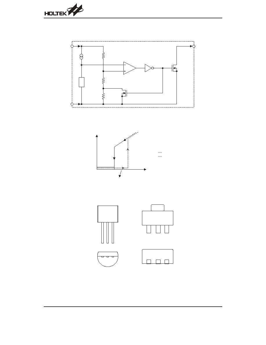
Functional Description
The HT7022A is a voltage detector equipped with a high
stability voltage reference which is connected to the
negative input of a comparator
æ denoted as V
REF
in the
following figure for NMOS output voltage detector.
When the voltage drop to the positive input of the com-
parator (i,e,V
B
) is higher than V
REF
, VOUT goes high,
M1 turns off, and V
B
is expressed as V
BH
=V
DD
¥
(R
B
+R
C
) / (R
A
+R
B
+R
C
). If V
DD
is decreased so that V
B
falls to a value less than V
REF
, the comparator output in-
verts from high to low, V
OUT
goes low, V
C
is high, M1
turns on, RC is bypassed, and V
B
becomes:
V
BL
=V
DD
¥R
B
/ (R
A
+R
B
), which is less than V
BH.
By so
doing, the comparator output will stay low to prevent the
circuit from oscillating when V
B
ª V
REF.
If V
DD
falls below the minimum operating voltage, the
output becomes undefined. When VDD goes from low to
V
DD
¥ R
B
/ (R
A
+R
B
) > V
REF
, the comparator output and
V
OUT
goes high.
The detectable voltage is defined as:
V
DET
(
-) =
R + R + R
R + R
A
B
C
B
C
¥ V
REF
The release voltage is defined as:
V
DET
(+) =
R + R
R
A
B
B
¥ V
REF
The hysteresis width is:
V
HYS
= V
DET
(+)
- V
DET
(
-)
The figure demonstrates the NMOS output type with
positive output polarity (V
OUT
is normally open, active
low).
V
S S
V
D D
R
A
R
B
R
C
M 1
M N
C o m p a r a t o r
V
O U T
R
L
V
R E F
V
B
V
C
NMOS Output Voltage Detector
Application Circuits
Microcomputer Reset Circuit
Normally a reset circuit is required to protect the micro-
computer system from malfunctions due to power line
interruptions. The following examples show how differ-
ent output configurations perform a reset function in var-
ious systems.
∑
NMOS open drain output application for separate
power supply
∑
NMOS open drain output application with R-C delay
H T 7 0 2 2 A
V
D D
V
S S
V
O U T
M i c r o -
c o m p u t e r
C
R
V
D D 2
V
D D 1
R E S E T
H T 7 0 2 2 A
V
S S
V
O U T
M i c r o -
c o m p u t e r

HT7022A
Rev. 1.10
5
April 20, 2004
Power-on Reset Circuit
With several external components, the HT7022A can be
used to perform a power-on reset function as shown:
Change of Detectable Voltage
If the required voltage is not found in the standard prod-
uct selection table, it is possible to change it by using ex-
ternal resistance dividers or diodes.
∑
Varying the detectable voltage with a resistance di-
vider
Detectable voltage =
R + R
R
A
B
B
¥ V
DET
Hysteresis width =
R + R
R
A
B
B
¥ V
HYS
∑
Varying the detectable voltage with a diode
Detectable Voltage = V
f1
+V
f2
+V
DET
Malfunction Analysis
The following circuit demonstrates the way a circuit ana-
lyzes malfunctions by monitoring the variation or spike
noise of power supply voltage.
Charge Monitoring Circuit
The following circuit shows a charged monitor for pro-
tection against battery deterioration by overcharging.
When the voltage of the battery is higher than the set de-
tectable voltage, the transistor turns on to bypass the
charge current, protecting the battery from overcharg-
ing.
H T 7 0 2 2 A
V
O U T
V
S S
R
D
V
I N
V
D D
C
t
V
D D
t
V
O U T
V
O U T
V
S S
H T 7 0 2 2 A
V
S S
V
I N
V
S S
V
O U T
V
D D
R
A
R
B
H T 7 0 2 2 A
V
D D
V
I N
V
S S
V f 1
V f 2
V
O U T
V
S S
H T 7 0 2 2 A
V
O U T
V
S S
V
D D
V
S S
H T 7 0 2 2 A
V
D D
V
O U T
V
S S
L o a d
B A T T
S o l a r
C e l l
T r