 | ÐлекÑÑоннÑй компоненÑ: HT7733 | СкаÑаÑÑ:  PDF PDF  ZIP ZIP |
Äîêóìåíòàöèÿ è îïèñàíèÿ www.docs.chipfind.ru
HT77XX
PFM Step-up DC/DC Converter
Selection Table
Part No.
Output Voltage
Package
Marking
HT7727
2.7V
TO-92
SOT-89
SOT-25
HT77XX (for TO-92)
HT77XX# (for SOT-89)
77XX# (for SOT-25)
HT7730
3.0V
HT7733
3.3V
HT7737
3.7V
HT7750
5.0V
Note:
²XX² stands for output voltages.
Only lead free devices are available.
²#² stands for lead free devices. For the TO-92 package, there will be a
²#² mark at the end of the date code.
Rev 1.10
1
March 7, 2006
Features
·
Low start-up voltage: 0.6V (Typ.)
·
High efficiency: 85% (Typ.)
·
High output voltage accuracy:
±2.5%
·
Output voltage: 2.7V, 3.0V, 3.3V, 3.7V, 5.0V
·
Ultra low supply current I
DD2
: 4
mA (Typ.)
·
Low ripple and low noise
·
Low shutdown current: 0.5
mA (Typ.)
·
TO-92, SOT-89 and SOT-25 package
Applications
·
Palmtops/PDAs
·
Portable communicators/Smartphones
·
Cameras/Camcorders
·
Battery-powered equipment
General Description
The HT77XX series is a set of PFM step-up DC/DC con-
verter with high efficiency and low ripple. The series fea-
tures extremely low start-up voltage and high output
voltage accuracy. They require only three external com-
ponents to provide a fixed output voltage of 2.7V, 3.0V,
3.3V, 3.7V or 5.0V. CMOS technology ensures ultra low
supply current and makes them ideal for bat-
tery-operated applications powered from one or more
cells.
The HT77XX consists of an oscillator, a PFM control cir-
cuit, a driver transistor, a reference voltage unit, and a
high speed comparator. They employ pulse frequency
modulation (PFM) for minimum supply current and rip-
ple at light output loading. These devices are available
in space saving TO-92, SOT-89 and SOT-25 packages.
For SOT-25 package, it also build-in a chip enable func-
tion to reduce power consumption during shutdown
mode.
Technical Document
·
Tools Information
·
FAQs
·
Application Note
Block Diagram
Pin Assignment
Pin Description
Pin No.
Pin Name
Description
TO-92
SOT-25
SOT-89
¾
1
¾
CE
Chip enable pin, high active
2
2
2
VOUT
DC/DC converter output monitoring pin
¾
3
¾
NC
No connection
1
4
1
GND
Ground pin
3
5
3
LX
Switching pin
Absolute Maximum Ratings
Supply Voltage ..............................V
SS
-0.3V to V
SS
+7V
Storage Temperature ............................
-50°C to 125°C
Power Consumption (*1) .................................. 500mW
Operating Temperature...............................0
°C to 70°C
Power Consumption (*2) .................................. 250mW
Note: These are stress ratings only. Stresses exceeding the range specified under
²Absolute Maximum Ratings² may
cause substantial damage to the device. Functional operation of this device at other conditions beyond those
listed in the specification is not implied and prolonged exposure to extreme conditions may affect device reliabil-
ity.
*1: applied to SOT-89 and TO-92
*2: applied to SOT-25
HT77XX
Rev 1.10
2
March 7, 2006
G N D
S O T - 8 9
F r o n t V i e w
B o t t o m V i e w
S O T - 2 5
C E
V O U T
G N D
V O U T
T o p V i e w
H T 7 7 X X
7 7 X X
T O - 9 2
V O U T
G N D
H T 7 7 X X
L X
V O U T
L X
L X
L X
G N D
N C
C E
V O U T
N C
1
2
3
1
2
3
1
2
3
4
5
V O U T
G N D
V r e f
P F M C o n t r o l
O S C 1 1 5 k H z
B u f f e r
L X
C h i p E n a b l e
C E
Electrical Characteristics
HT7727, +2.7V Output Type
V
IN
=V
OUT
´0.6; I
OUT
=10mA; Ta=25
°C (Unless otherwise specified)
Symbol
Parameter
Test Conditions
Min.
Typ.
Max.
Unit
V
OUT
Output Voltage
¾
2.633
2.7
2.767
V
V
IN
Input Voltage
¾
¾
¾
6
V
V
START
Start-up Voltage
V
IN
: 0
®2V; I
OUT
=1mA
¾
0.6
0.7
V
V
HOLD
Minimum Hold-on Voltage
V
IN
: 2
®0V; I
OUT
=1mA
¾
¾
0.7
V
I
IN
No load Input Current
Measured at no load
¾
10
¾
mA
I
DD1
Supply Current 1
V
IN
=V
OUT
´0.95
Measured at VOUT pin
¾
40
¾
mA
I
DD2
Supply Current 2
V
IN
=V
OUT
+0.5V
Measured at VOUT pin
¾
4
7
mA
I
SHDN
Shutdown Current
V
CE
=V
IL
, V
IN
=V
OUT
´0.95
¾
0.5
¾
mA
I
LEAK
LX Leakage Current
V
IN
=6V
¾
¾
0.9
mA
f
OSC
Maximum Oscillator Frequency
V
IN
=V
OUT
´0.95
Measured at LX pin
¾
115
¾
kHz
h
Efficiency
¾
¾
85
¾
%
D
OSC
Oscillator Duty Cycle
V
IN
=V
OUT
´0.95
Measured at LX pin
65
75
85
%
HT7730, +3.0V Output Type
V
IN
=V
OUT
´0.6; I
OUT
=10mA; Ta=25
°C (Unless otherwise specified)
Symbol
Parameter
Test Conditions
Min.
Typ.
Max.
Unit
V
OUT
Output Voltage
¾
2.925
3
3.075
V
V
IN
Input Voltage
¾
¾
¾
6
V
V
START
Start-up Voltage
V
IN
: 0
®2V; I
OUT
=1mA
¾
0.6
0.7
V
V
HOLD
Min. Hold-on Voltage
V
IN
: 2
®0V; I
OUT
=1mA
¾
¾
0.7
V
I
IN
No load Input Current
Measured at no load
¾
10
¾
mA
I
DD1
Supply Current 1
V
IN
=V
OUT
´0.95
Measured at VOUT pin
¾
48
¾
mA
I
DD2
Supply Current 2
V
IN
=V
OUT
+0.5V
Measured at VOUT pin
¾
4
7
mA
I
SHDN
Shutdown Current
V
CE
=V
IL
, V
IN
=V
OUT
´0.95
¾
0.5
¾
mA
I
LEAK
LX Leakage Current
V
IN
=6V
¾
¾
0.9
mA
f
OSC
Maximum Oscillator Frequency
V
IN
=V
OUT
´0.95
Measured at LX pin
¾
115
¾
kHz
h
Efficiency
¾
¾
85
¾
%
D
OSC
Oscillator Duty Cycle
V
IN
=V
OUT
´0.95
Measured at LX pin
65
75
85
%
HT77XX
Rev 1.10
3
March 7, 2006
HT7733, +3.3V Output Type
V
IN
=V
OUT
´0.6; I
OUT
=10mA; Ta=25
°C (Unless otherwise specified)
Symbol
Parameter
Test Conditions
Min.
Typ.
Max.
Unit
V
OUT
Output Voltage
¾
3.218
3.3
3.382
V
V
IN
Input Voltage
¾
¾
¾
6
V
V
START
Start-up Voltage
V
IN
: 0
®2V; I
OUT
=1mA
¾
0.6
0.7
V
V
HOLD
Min. Hold-on Voltage
V
IN
: 2
®0V; I
OUT
=1mA
¾
¾
0.7
V
I
IN
No load Input Current
Measured at no load
¾
10
¾
mA
I
DD1
Supply Current 1
V
IN
=V
OUT
´0.95
Measured at VOUT pin
¾
60
¾
mA
I
DD2
Supply Current 2
V
IN
=V
OUT
+0.5V
Measured at VOUT pin
¾
4
7
mA
I
SHDN
Shutdown Current
V
CE
=V
IL
, V
IN
=V
OUT
´0.95
¾
0.5
¾
mA
I
LEAK
LX Leakage Current
V
IN
=6V
¾
¾
0.9
mA
f
OSC
Maximum Oscillator Frequency
V
IN
=V
OUT
´0.95
Measured at LX pin
¾
115
¾
kHz
h
Efficiency
¾
¾
85
¾
%
D
OSC
Oscillator Duty Cycle
V
IN
=V
OUT
´0.95
Measured at LX pin
65
75
85
%
HT7737, +3.7V Output Type
V
IN
=V
OUT
´0.6; I
OUT
=10mA; Ta=25
°C (Unless otherwise specified)
Symbol
Parameter
Test Conditions
Min.
Typ.
Max.
Unit
V
OUT
Output Voltage
¾
3.608
3.7
3.793
V
V
IN
Input Voltage
¾
¾
¾
6
V
V
START
Start-up Voltage
V
IN
: 0
®2V; I
OUT
=1mA
¾
0.6
0.7
V
V
HOLD
Min. Hold-on Voltage
V
IN
: 2
®0V; I
OUT
=1mA
¾
¾
0.7
V
I
IN
No load Input Current
Measured at no load
¾
10
¾
mA
I
DD1
Supply Current 1
V
IN
=V
OUT
´0.95
Measured at VOUT pin
¾
64
¾
mA
I
DD2
Supply Current 2
V
IN
=V
OUT
+0.5V
Measured at VOUT pin
¾
4
7
mA
I
SHDN
Shutdown Current
V
CE
=V
IL
, V
IN
=V
OUT
´0.95
¾
0.5
¾
mA
I
LEAK
LX Leakage Current
V
IN
=6V
¾
¾
0.9
mA
f
OSC
Maximum Oscillator Frequency
V
IN
=V
OUT
´0.95
Measured at LX pin
¾
115
¾
kHz
h
Efficiency
¾
¾
85
¾
%
D
OSC
Oscillator Duty Cycle
V
IN
=V
OUT
´0.95
Measured at LX pin
65
75
85
%
HT77XX
Rev 1.10
4
March 7, 2006
HT7750, +5.0V Output Type
V
IN
=V
OUT
´0.6; I
OUT
=10mA; Ta=25
°C (Unless otherwise specified)
Symbol
Parameter
Test Conditions
Min.
Typ.
Max.
Unit
V
OUT
Output Voltage
¾
4.875
5
5.125
V
V
IN
Input Voltage
¾
¾
¾
6
V
V
START
Start-up Voltage
V
IN
: 0
®2V; I
OUT
=1mA
¾
0.7
0.8
V
V
HOLD
Min. Hold-on Voltage
V
IN
: 2
®0V; I
OUT
=1mA
¾
¾
0.7
V
I
IN
Current Consumption
Measured at no load
¾
10
¾
mA
I
DD1
Supply Current 1
V
IN
=V
OUT
´0.95
Measured at VOUT pin
¾
85
¾
mA
I
DD2
Supply Current 2
V
IN
=V
OUT
+0.5V
Measured at VOUT pin
¾
4
7
mA
I
SHDN
Shutdown Current
V
CE
=V
IL
, V
IN
=V
OUT
´0.95
¾
0.5
¾
mA
I
LEAK
LX Leakage Current
V
IN
=6V
¾
¾
0.9
mA
f
OSC
Maximum Oscillator Frequency
V
IN
=V
OUT
´0.95
Measured at LX pin
¾
115
¾
kHz
h
Efficiency
¾
¾
85
¾
%
D
OSC
Oscillator Duty Cycle
V
IN
=V
OUT
´0.95
Measured at LX pin
65
75
85
%
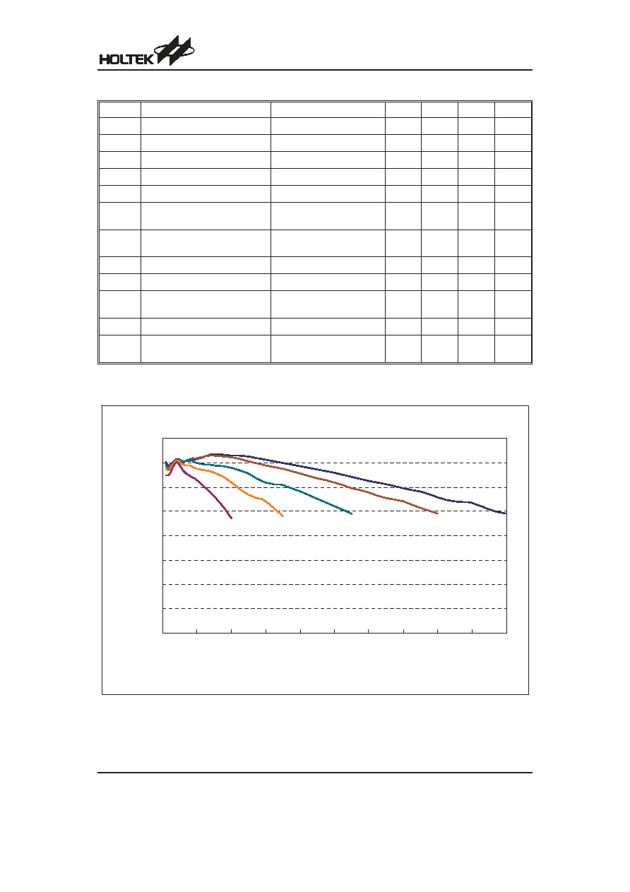
Typical Performance Characteristics
L=220
mH, C=47mF
HT7730 Efficiency vs. Output Current
HT77XX
Rev 1.10
5
March 7, 2006
5 0
5 5
6 0
6 5
7 0
7 5
8 0
8 5
9 0
0
1 0
2 0
3 0
4 0
5 0
6 0
7 0
8 0
9 0
1 0 0
O u t p u t C u r r e n t ( m A )
E
f
f
i
c
i
e
n
c
y
(
%
)
V
I N
= 0 . 9 V
V
I N
= 1 . 2 V
V
I N
= 1 . 5 V
V
I N
= 1 . 8 V
V
I N
= 2 . 0 V
L=220
mH, C=47mF
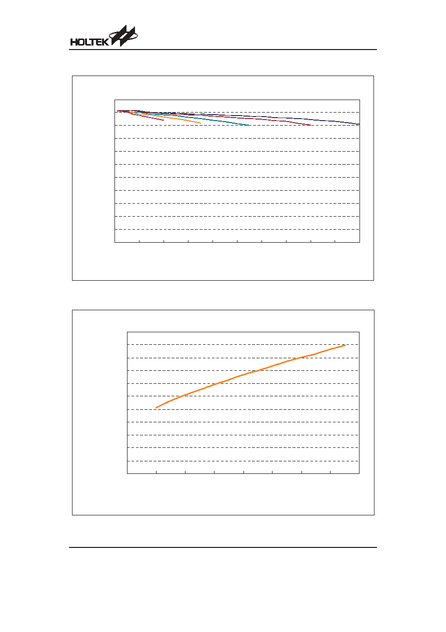
HT7730 Output Voltage vs. Output Current
L=220
mH, C=47mF
HT7730 Maximum Oscillator Frequency vs. Temperature
HT77XX
Rev 1.10
6
March 7, 2006
O u t p u t C u r r e n t ( m A )
O
u
t
p
u
t
V
o
l
t
a
g
e
(
V
)
V
I N
= 0 . 9 V
V
I N
= 1 . 2 V
V
I N
= 1 . 5 V
V
I N
= 1 . 8 V
V
I N
= 2 . 0 V
2
2 . 1
2 . 2
2 . 3
2 . 4
2 . 5
2 . 6
2 . 7
2 . 8
2 . 9
3
3 . 1
0
1 0
2 0
3 0
4 0
5 0
6 0
7 0
8 0
9 0
1 0 0
4 0
5 0
6 0
7 0
8 0
9 0
1 0 0
1 1 0
1 2 0
1 3 0
1 4 0
1 5 0
- 6 0
- 4 0
- 2 0
0
2 0
4 0
6 0
8 0
1 0 0
T e m p e r a t u r e ( ° C )
M
a
x
i
m
u
m
O
s
c
i
l
l
a
t
o
r
F
r
e
q
u
e
n
c
y
(
k
H
z
)
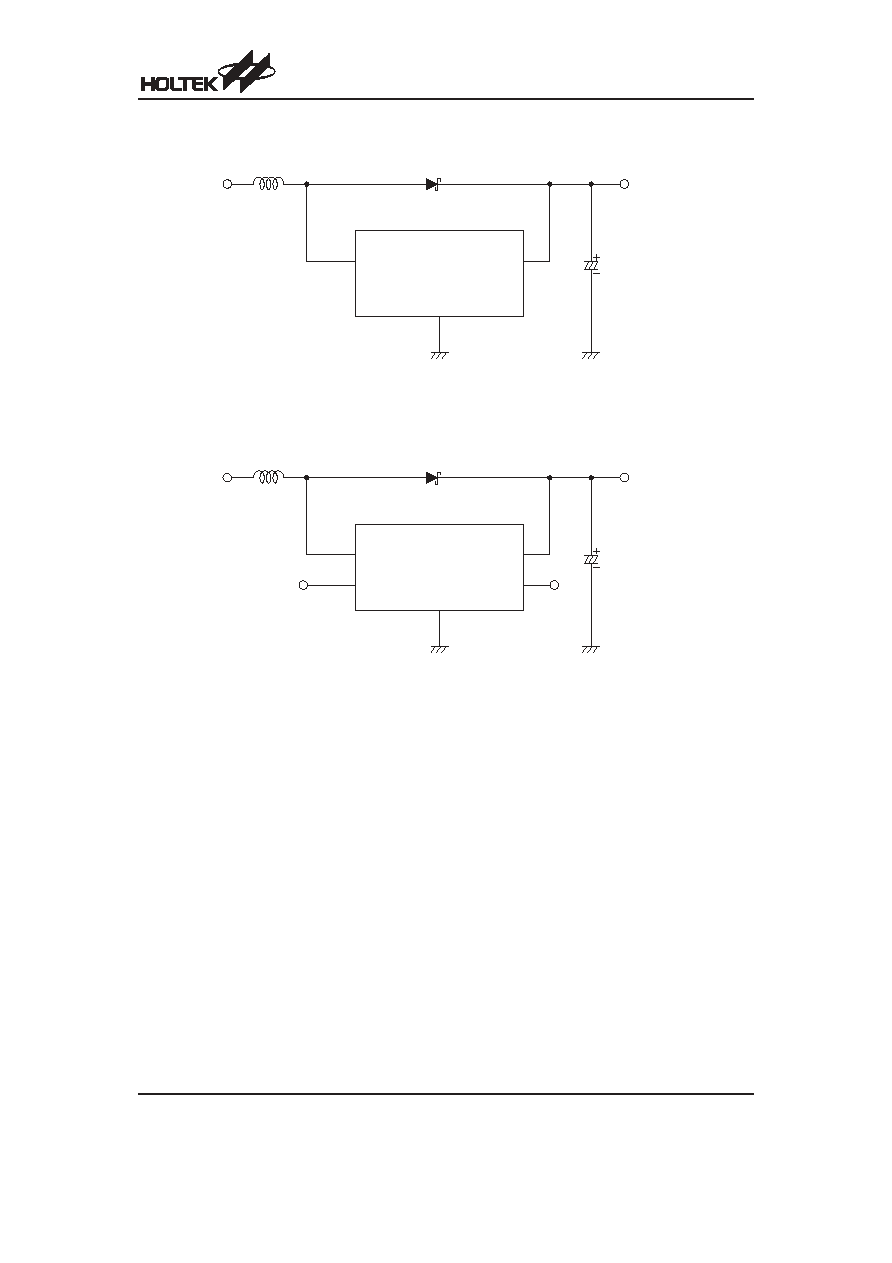
Application Circuits
Note:
For the SOT-25 package, when CE is pulled low, the internal blocks of the device, such as the reference band
gap, gain block, and all feedback and control circuitry will be switched off. The boost converter
¢s output, VOUT,
will be at a value one Schottky diode voltage drop below the input voltage and the LX pin remains in a high im-
pedance condition. The output capacitor and load at VOUT determine the rate at which VOUT decays.
HT77XX
Rev 1.10
7
March 7, 2006
S u m i d a C D - 5 4
V
I N
L X
V O U T
H T 7 7 X X
S e r i e s
G N D
2 2 m F
V
O U T
T O - 9 2 / S O T - 8 9
1 0 0 m H
I N 5 8 1 9
S u m i d a C D - 5 4
V
I N
L X
V O U T
H T 7 7 X X
S e r i e s
G N D
2 2 m F
V
O U T
S O T - 2 5
1 0 0 m H
I N 5 8 1 9
C E
N C
Package Information
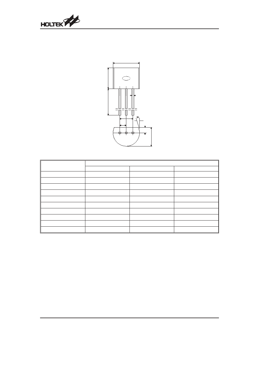
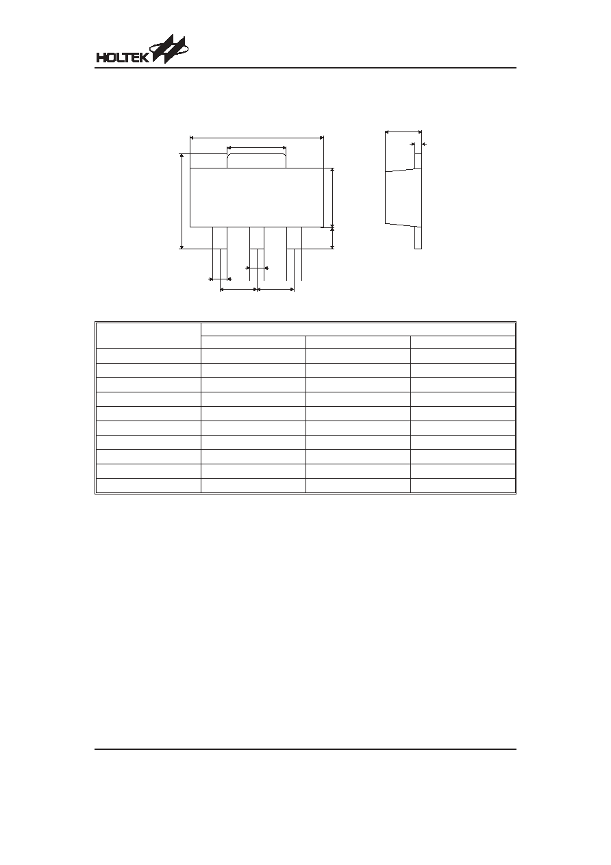
3-pin TO-92 Outline Dimensions
Symbol
Dimensions in mil
Min.
Nom.
Max.
A
170
¾
200
B
170
¾
200
C
500
¾
¾
D
11
¾
20
E
90
¾
110
F
45
¾
55
G
45
¾
65
H
130
¾
160
I
8
¾
18
a
4
°
¾
6
°
HT77XX
Rev 1.10
8
March 7, 2006
A
B
C
E
F
G
H
D
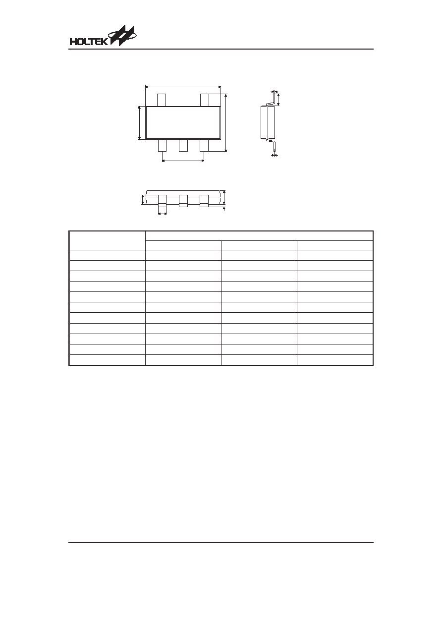
3-pin SOT-89 Outline Dimensions
Symbol
Dimensions in mil
Min.
Nom.
Max.
A
173
¾
181
B
64
¾
72
C
90
¾
102
D
35
¾
47
E
155
¾
167
F
14
¾
19
G
17
¾
22
H
¾
59
¾
I
55
¾
63
J
14
¾
17
HT77XX
Rev 1.10
9
March 7, 2006
A
E
B
C
D
H
G
F
I
J
5-pin SOT-25 Outline Dimensions
Symbol
Dimensions in mm
Min.
Nom.
Max.
A
1.00
¾
1.30
A1
¾
¾
0.10
A2
0.70
¾
0.90
b
0.35
¾
0.50
C
0.10
¾
0.25
D
2.70
¾
3.10
E
1.40
¾
1.80
e
¾
1.90
¾
H
2.60
¾
3
L
0.37
¾
¾
q
1
°
¾
9
°
HT77XX
Rev 1.10
10
March 7, 2006
D
H
E
e
A 2
b
A 1
A
C
L
q
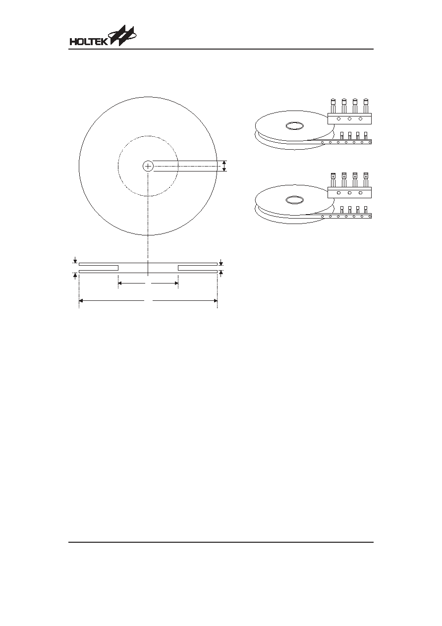
Product Tape and Reel Specifications
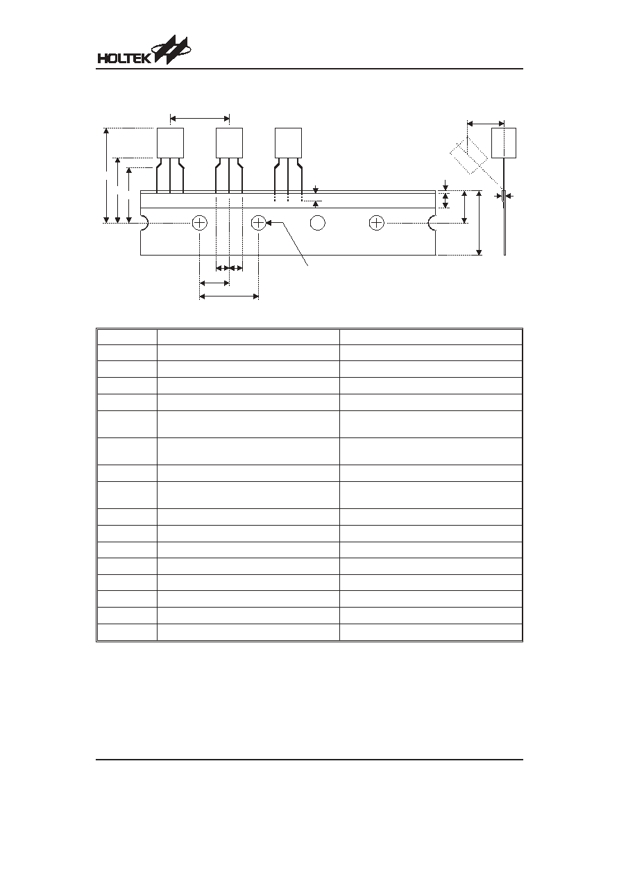
TO-92 Reel Dimensions (Unit: mm)
HT77XX
Rev 1.10
11
March 7, 2006
5 8
P a c k a g e U p , F l a t S i d e U p
P a c k a g e U p , F l a t S i d e D o w n
3 6 0
8 8
3 0
4 3
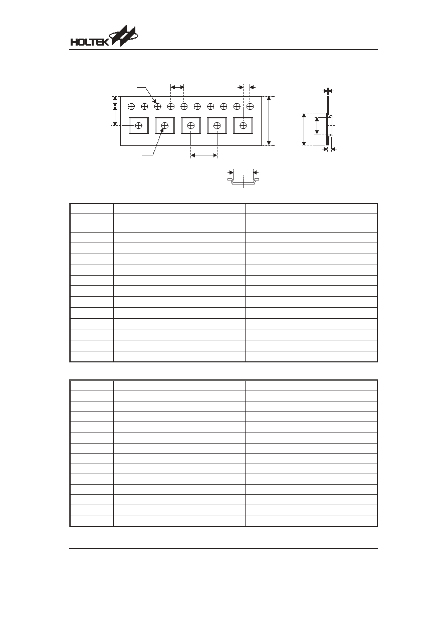
SOT-89 & SOT-25 Reel Dimensions
SOT-89
Symbol
Description
Dimensions in mm
A
Reel Outer Diameter
180
±1.0
B
Reel Inner Diameter
62
±1.5
C
Spindle Hole Diameter
12.75+0.15
D
Key Slit Width
1.9
±0.15
T1
Space Between Flange
12.4+0.2
T2
Reel Thickness
17
-0.4
SOT-25
Symbol
Description
Dimensions in mm
A
Reel Outer Diameter
178
±1.0
B
Reel Inner Diameter
62
±1.0
C
Spindle Hole Diameter
13.0
±0.2
D
Key Slit Width
2.5
±0.25
T1
Space Between Flange
8.4+1.5
-0.0
T2
Reel Thickness
11.4+1.5
HT77XX
Rev 1.10
12
March 7, 2006
A
C
B
T 1
T 2
D
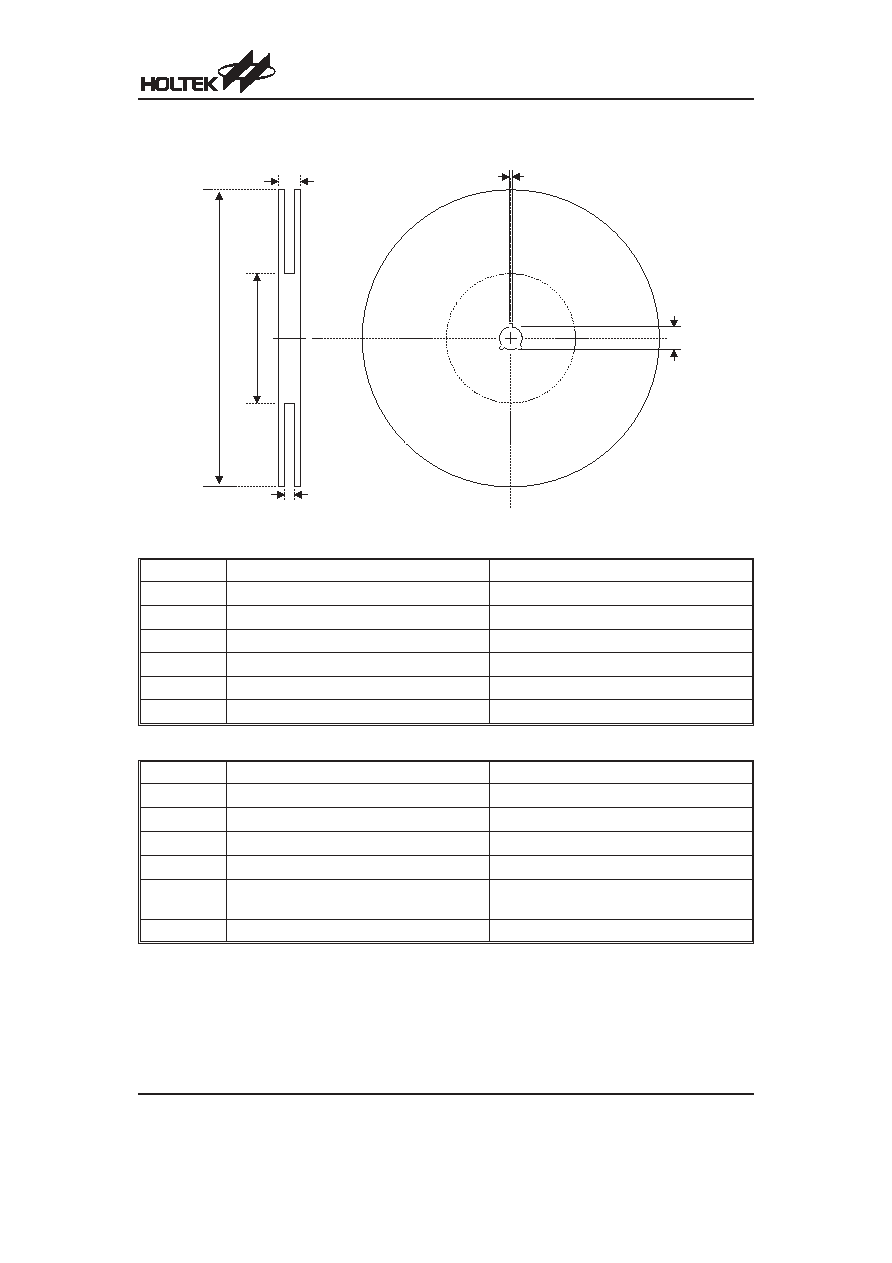
TO-92 Carrier Tape Dimensions
TO-92
Symbol
Description
Dimensions in mm
I1
Taped Lead Length
(2.5)
P
Component Pitch
12.7
±1.0
P
0
Perforation Pitch
12.7
±0.3
P
2
Component to Perforation (Length Direction)
6.35
±0.4
F
1
Lead Spread
2.5+0.4
-0.1
F
2
Lead Spread
2.5+0.4
-0.1
Dh
Component Alignment
0
±0.1
W
Carrier Tape Width
18.0+1.0
-0.5
W
0
Hold-down Tape Width
6.0
±0.5
W
1
Perforation Position
9.0
±0.5
W
2
Hold-down Tape Position
(0.5)
H
0
Lead Clinch Height
16.0
±0.5
H
1
Component Height
Less than 24.7
D
0
Perforation Diameter
4.0
±0.2
t
Taped Lead Thickness
0.7
±0.2
H
Component Base Height
19.0
±0.5
Note:
Thickness less than 0.38
±0.05mm~0.5mm
P0 Accumulated pitch tolerance:
±1mm/20pitches.
( ) Bracketed figures are for reference only.
HT77XX
Rev 1.10
13
March 7, 2006
F 1 F 2
P 2
P 0
D 0
W 2
W 0
W
W 1
P
H 0
H
H 1
t
D h
l 1
SOT-89 & SOT-25 Carrier Tape Dimensions
SOT-89
Symbol
Description
Dimensions in mm
W
Carrier Tape Width
12.0+0.3
-0.1
P
Cavity Pitch
8.0
±0.1
E
Perforation Position
1.75
±0.1
F
Cavity to Perforation (Width Direction)
5.5
±0.05
D
Perforation Diameter
1.5+0.1
D1
Cavity Hole Diameter
1.5+0.1
P0
Perforation Pitch
4.0
±0.1
P1
Cavity to Perforation (Length Direction)
2.0
±0.10
A0
Cavity Length
4.8
±0.1
B0
Cavity Width
4.5
±0.1
K0
Cavity Depth
1.8
±0.1
t
Carrier Tape Thickness
0.30
±0.013
C
Cover Tape Width
9.3
SOT-25
Symbol
Description
Dimensions in mm
W
Carrier Tape Width
8.0
±0.3
P
Cavity Pitch
4.0
E
Perforation Position
1.75
F
Cavity to Perforation (Width Direction)
3.5
±0.05
D
Perforation Diameter
1.5+0.1
D1
Cavity Hole Diameter
1.5+0.1
P0
Perforation Pitch
4.0
P1
Cavity to Perforation (Length Direction)
2.0
A0
Cavity Length
3.15
B0
Cavity Width
3.2
K0
Cavity Depth
1.4
t
Carrier Tape Thickness
0.20
±0.03
C
Cover Tape Width
5.3
HT77XX
Rev 1.10
14
March 7, 2006
P
D 1
W
P 1
P 0
D
E
F
t
K 0
B 0
A 0
C

HT77XX
Rev 1.10
15
March 7, 2006
Copyright
Ó 2006 by HOLTEK SEMICONDUCTOR INC.
The information appearing in this Data Sheet is believed to be accurate at the time of publication. However, Holtek as-
sumes no responsibility arising from the use of the specifications described. The applications mentioned herein are used
solely for the purpose of illustration and Holtek makes no warranty or representation that such applications will be suitable
without further modification, nor recommends the use of its products for application that may present a risk to human life
due to malfunction or otherwise. Holtek
¢s products are not authorized for use as critical components in life support devices
or systems. Holtek reserves the right to alter its products without prior notification. For the most up-to-date information,
please visit our web site at http://www.holtek.com.tw.
Holtek Semiconductor Inc. (Headquarters)
No.3, Creation Rd. II, Science Park, Hsinchu, Taiwan
Tel: 886-3-563-1999
Fax: 886-3-563-1189
http://www.holtek.com.tw
Holtek Semiconductor Inc. (Taipei Sales Office)
4F-2, No. 3-2, YuanQu St., Nankang Software Park, Taipei 115, Taiwan
Tel: 886-2-2655-7070
Fax: 886-2-2655-7373
Fax: 886-2-2655-7383 (International sales hotline)
Holtek Semiconductor Inc. (Shanghai Sales Office)
7th Floor, Building 2, No.889, Yi Shan Rd., Shanghai, China 200233
Tel: 021-6485-5560
Fax: 021-6485-0313
http://www.holtek.com.cn
Holtek Semiconductor Inc. (Shenzhen Sales Office)
43F, SEG Plaza, Shen Nan Zhong Road, Shenzhen, China 518031
Tel: 0755-8346-5589
Fax: 0755-8346-5590
ISDN: 0755-8346-5591
Holtek Semiconductor Inc. (Beijing Sales Office)
Suite 1721, Jinyu Tower, A129 West Xuan Wu Men Street, Xicheng District, Beijing, China 100031
Tel: 010-6641-0030, 6641-7751, 6641-7752
Fax: 010-6641-0125
Holmate Semiconductor, Inc. (North America Sales Office)
46712 Fremont Blvd., Fremont, CA 94538
Tel: 510-252-9880
Fax: 510-252-9885
http://www.holmate.com
Document Outline
- þÿ
- þÿ
- þÿ
- þÿ
- þÿ
- þÿ
- þÿ
- þÿ
- þÿ
- þÿ
- þÿ
- þÿ
- þÿ
- þÿ