 | ÐлекÑÑоннÑй компоненÑ: HT82K95EE | СкаÑаÑÑ:  PDF PDF  ZIP ZIP |
HT82K95EE/HT82K95AE --
USB Multimedia Keyboard Encoder 8-Bit MCU

HT82K95EE/HT82K95AE
USB Multimedia Keyboard Encoder 8-Bit MCU
Rev. 1.00
1
February 15, 2006
General Description
This device is an 8-bit high performance RISC architec-
ture microcontroller designed for USB product applica-
tions. It is particularly suitable for use in products such
as keyboards. A HALT feature is included to reduce
power consumption. The mask version HT82K95AE is
fully pin and functionally compatible with the OTP ver-
sion HT82K95EE device.
There are two dice in the HT82K95EE/HT82K95AE
package: one is the HT82K95E/HT82K95A MCU, the
other is a 128
´8 bits EEPROM used for data memory
purpose. The two dice are wire-bonded to form
HT82K95EE/HT82K95AE.
Features
·
Operating voltage:
f
SYS
=6M/12MHz: 4.2V~5.5V
·
Low voltage reset function
·
32 bidirectional I/O lines (max.)
·
8-bit programmable timer/event counter with over-
flow interrupt
·
16-bit programmable timer/event counter and over-
flow interrupts
·
Crystal oscillator (6MHz or 12MHz)
·
Watchdog Timer
·
PS2 and USB modes supported
·
USB1.1 low speed function
·
3 endpoints supported (endpoint 0 included)
·
4096
´15 program memory ROM
·
160
´8 data memory RAM
·
128
´8 data EEPROM
·
All I/O ports support wake-up options
·
HALT function and wake-up feature reduce power
consumption
·
8-level subroutine nesting
·
Up to 0.33
ms instruction cycle with 12MHz system
clock at V
DD
=5V
·
Bit manipulation instruction
·
15-bit table read instruction
·
63 powerful instructions
·
All instructions in one or two machine cycles
·
20/28-pin SOP package
Technical Document
·
Tools Information
·
FAQs
·
Application Note
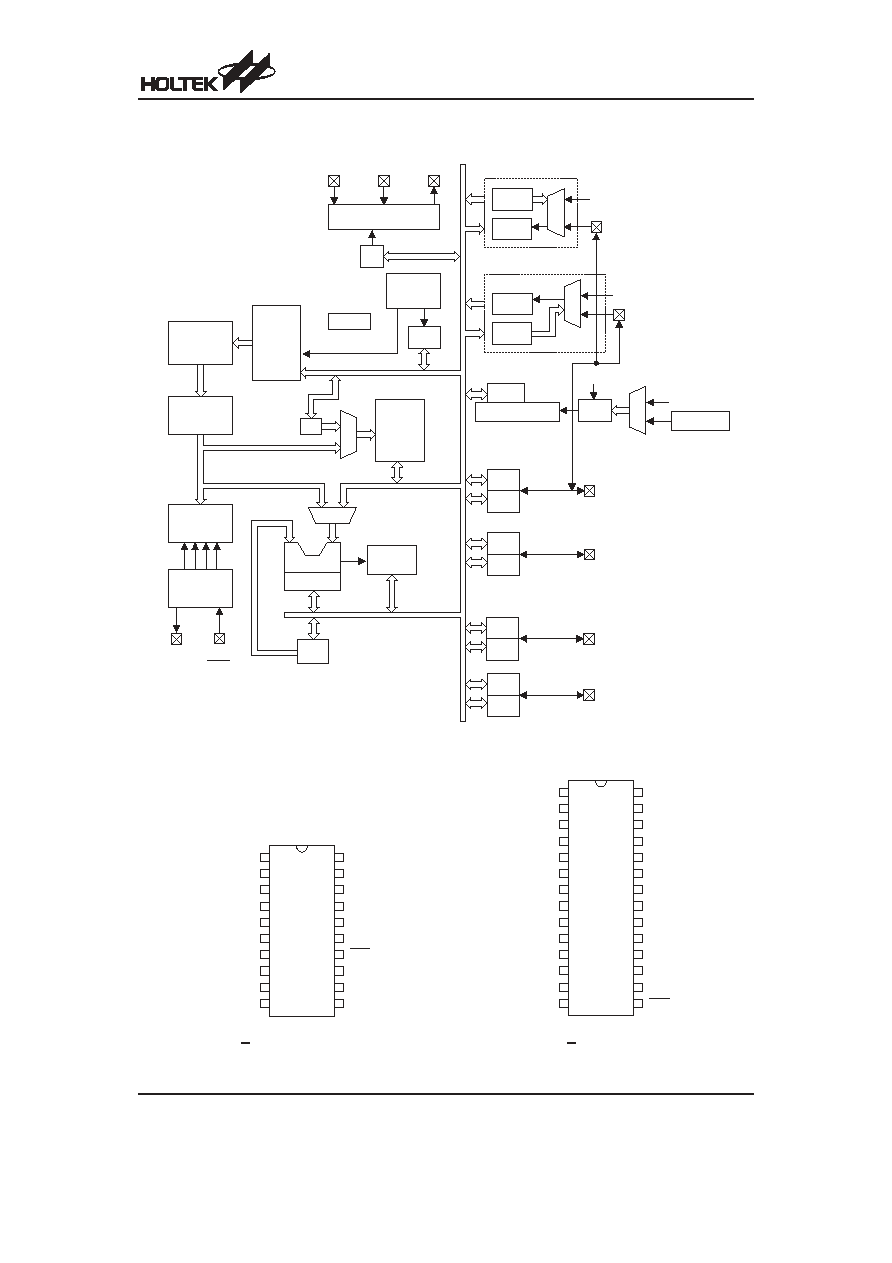
Block Diagram
Pin Assignment
HT82K95EE/HT82K95AE
Rev. 1.00
2
February 15, 2006
O S C 2
O S C 1
R E S
V D D
M U X
T M R 0 C
T M R 0
V S S
P r o g r a m
R O M
P r o g r a m
C o u n t e r
I n t e r r u p t
C i r c u i t
S T A C K
I N T C
D a t a
M e m o r y
I n s t r u c t i o n
R e g i s t e r
M
U
X
I n s t r u c t i o n
D e c o d e r
S T A T U S
A L U
S h i f t e r
T i m i n g
G e n e r a t o r
A C C
M
U
X
M P
S Y S C L K / 4
W D T S
W D T
W D T O S C
W D T P r e s c a l e r
M
U
X
E N / D I S
P D C
P O R T D
P D 0 ~ P D 7
P B C
P O R T B
P B 0 ~ P B 5
P B 6 / S C L
P B 7 / S D A
P B
P A C
P O R T A
P A 0 ~ P A 5
P A 6 / T M R 0
P A 7 / T M R 1
P A
P D
P C
P O R T C
P C 0 ~ P C 7
P C C
T M R 1 C
T M R 1
M
U
X
P A 7 / T M R 1
f
S Y S
/ 4
f
S Y S
/ 4
P A 6 / T M R 0
U S B 1 . 1
P S 2
B P
U S B D + / C L K U S B D - / D A T A
V 3 3 O
P A 6
P A 7
2 0
1 9
1 8
1 7
1 6
1 5
1 4
1 3
1 2
1 1
1
2
3
4
5
6
7
8
9
1 0
H T 8 2 K 9 5 E E / H T 8 2 K 9 5 A E
2 0 S O P - A / S S O P - A
P A 3
P A 2
P A 1
P A 0
P C 0
P D 4
V D D
V 3 3 O
U S B D + / C L K
U S B D - / D A T A
P A 4
P A 5
P A 6 / T M R 0
P A 7 / T M R 1
O S C 1
O S C 2
R E S
V S S
P B 7 / S D A
P B 6 / S C L
2 8
2 7
2 6
2 5
2 4
2 3
2 2
2 1
2 0
1 9
1 8
1 7
1 6
1 5
1
2
3
4
5
6
7
8
9
1 0
1 1
1 2
1 3
1 4
H T 8 2 K 9 5 E E / H T 8 2 K 9 5 A E
2 8 S O P - A
P C 3
V D D
V 3 3 O
U S B D + / C L K
U S B D - / D A T A
P B 0
P B 1
P B 2
P B 3
P B 4
P B 5
P B 6 / S C L
P B 7 / S D A
V S S
P C 2
P C 0
P A 0
P A 1
P A 2
P A 3
P C 4
P A 4
P A 5
P A 6 / T M R 0
P A 7 / T M R 1
O S C 1
O S C 2
R E S
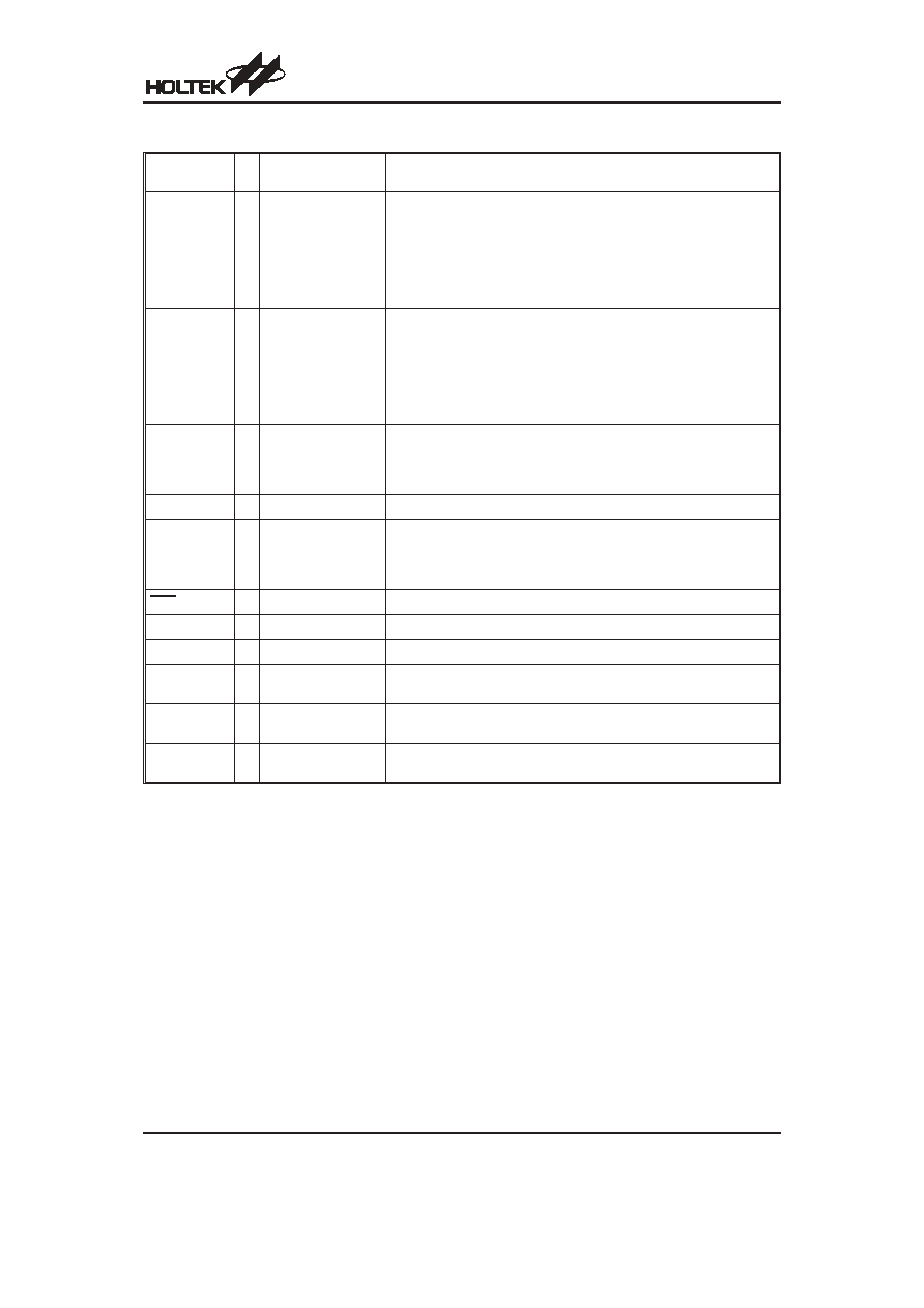
Pin Description
Pin Name
I/O
ROM Code
Option
Description
PA0~PA5
PA6/TMR0
PA7/TMR1
I/O
Pull-high
Wake-up
CMOS/NMOS/PMOS
Bidirectional 8-bit input/output port. Each bit can be configured as a
wake-up input by ROM code option. The input or output mode is con-
trolled by PAC (PA control register).
Pull-high resistor options: PA0~PA7
CMOS/NMOS/PMOS options: PA0~PA7
Wake up options: PA0~PA7
PA6 and PA7 are pin-shared with TMR0 and TMR1 input, respectively.
PB0~PB5
PB6/SCL
PB7/SDA
I/O
Pull-high
Wake-up
Bidirectional 8-bit input/output port. Software instructions determine the
CMOS output or Schmitt trigger input with pull-high resistor (determined
by pull-high options).
Wake-up options: PB0~PB5
Falling edge wake-up options: PB6, PB7
PB6 is wire-bonded with SCL pad of the Data EEPROM
PB7 is wire-bonded with SDA pad of the Data EEPROM
PD0~PD7
I/O
Pull-high
Wake-up
Bidirectional I/O lines. Software instructions determine the CMOS out-
put or Schmitt trigger input with pull-high resistor (determined by
pull-high options).
Wake-up options: PD0~PD7
VSS
¾
¾
Negative power supply, ground
PC0~PC7
I/O
Pull-high
Wake-up
Bidirectional I/O lines. Software instructions determine the CMOS out-
put or Schmitt trigger input with pull-high resistor (determined by
pull-high options).
Wake-up options: PC0~PC7
RES
I
¾
Schmitt trigger reset input. Active low
VDD
¾
¾
Positive power supply
V33O
O
¾
3.3V regulator output
USBD+/CLK
I/O
¾
USBD+ or PS2 CLK I/O line
USB or PS2 function is controlled by software control register
USBD-/DATA
I/O
¾
USBD- or PS2 DATA I/O line
USB or PS2 function is controlled by software control register
OSC1
OSC2
I
O
¾
OSC1, OSC2 are connected to a 6MHz or 12MHz Crystal/resonator
(determined by software instructions) for the internal system clock.
Absolute Maximum Ratings
Supply Voltage ...........................V
SS
-0.3V to V
SS
+6.0V
Storage Temperature ............................
-50°C to 125°C
Input Voltage..............................V
SS
-0.3V to V
DD
+0.3V
Operating Temperature...............................0
°C to 70°C
Note: These are stress ratings only. Stresses exceeding the range specified under
²Absolute Maximum Ratings² may
cause substantial damage to the device. Functional operation of this device at other conditions beyond those
listed in the specification is not implied and prolonged exposure to extreme conditions may affect device reliabil-
ity.
HT82K95EE/HT82K95AE
Rev. 1.00
3
February 15, 2006
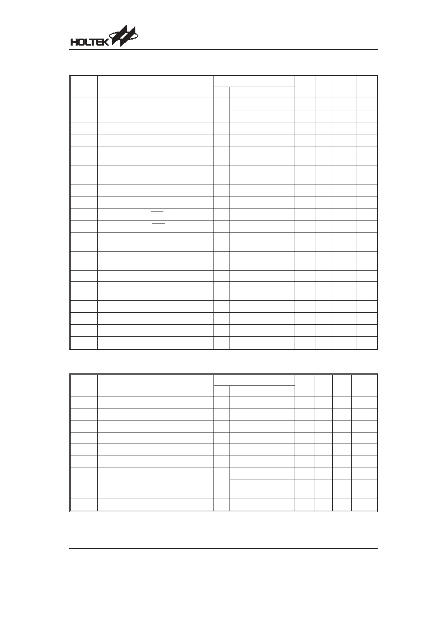
D.C. Characteristics
Ta=25
°C
Symbol
Parameter
Test Conditions
Min.
Typ.
Max.
Unit
V
DD
Conditions
V
DD
Operating Voltage
¾
f
SYS
=6MHz
4.2
¾
5.5
V
f
SYS
=12MHz
4.2
¾
5.5
V
I
DD1
Operating Current (6MHz Crystal)
5V
No load, f
SYS
=6MHz
¾
6.5
12
mA
I
DD2
Operating Current (12MHz Crystal)
5V
No load, f
SYS
=12MHz
¾
7.5
16
mA
I
STB1
Standby Current (WDT Enabled)
5V
No load, system HALT,
USB suspend
¾
¾
250
mA
I
STB2
Standby Current (WDT Disabled)
5V
No load, system HALT,
USB suspend
¾
¾
230
mA
V
IL1
Input Low Voltage for I/O Ports
5V
¾
0
¾
0.8
V
V
IH1
Input High Voltage for I/O Ports
5V
¾
2
¾
5
V
V
IL2
Input Low Voltage (RES)
5V
¾
0
¾ 0.4V
DD
V
V
IH2
Input High Voltage (RES)
5V
¾
0.9V
DD
¾
V
DD
V
I
OL1
I/O Port Sink Current for PA1~PA7, PB, PC,
PD
5V
V
OL
=3.4V
10
15
20
mA
I
OL2
I/O Port Sink Current for PA1~PA7, PB, PC,
PD
5V
V
OL
=0.4V
2
4
8
mA
I
OL3
I/O Port Sink Current for PA0
5V
V
OL
=0.4V
7
10
13
mA
I
OH1
I/O Port Source Current for PA1~PA7, PB,
PC, PD
5V
V
OH
=3.4V
-2
-4
-8
mA
I
OH2
I/O Port Source Current for PA0
5V
V
OH
=3.4V
-12
-18
-24
mA
R
PH
Pull-high Resistance for PA, PB, PC, PD
5V
¾
25
50
80
k
W
V
LVR
Low Voltage Reset
¾
¾
3
3.4
4.0
V
V
V33O
3.3V Regulator Output
5V
I
V33O
=
-5mA
3.0
3.3
3.6
V
A.C. Characteristics
Ta=25
°C
Symbol
Parameter
Test Conditions
Min.
Typ. Max.
Unit
V
DD
Conditions
f
SYS
System Clock (Crystal OSC)
5V
¾
6
¾
12
MHz
f
TIMER
Timer I/P Frequency (TMR)
5V
¾
0
¾
12
MHz
t
WDTOSC
Watchdog Oscillator
5V
¾
15
31
70
ms
t
WDT1
Watchdog Time-out Period (WDT OSC)
5V
Without WDT prescaler
4
8
16
ms
t
WDT2
Watchdog Time-out Period (System Clock)
¾ Without WDT prescaler
¾
1024
¾
t
SYS
t
RES
External Reset Low Pulse Width
¾
¾
1
¾
¾
ms
t
SST
System Start-up Timer Period
¾
Wake-up from HALT
¾
1024
¾
t
SYS
Power-up, Watchdog
Time-out from normal
¾
1024
¾
t
WDTOSC
t
INT
Interrupt Pulse Width
¾
¾
1
¾
¾
ms
HT82K95EE/HT82K95AE
Rev. 1.00
4
February 15, 2006
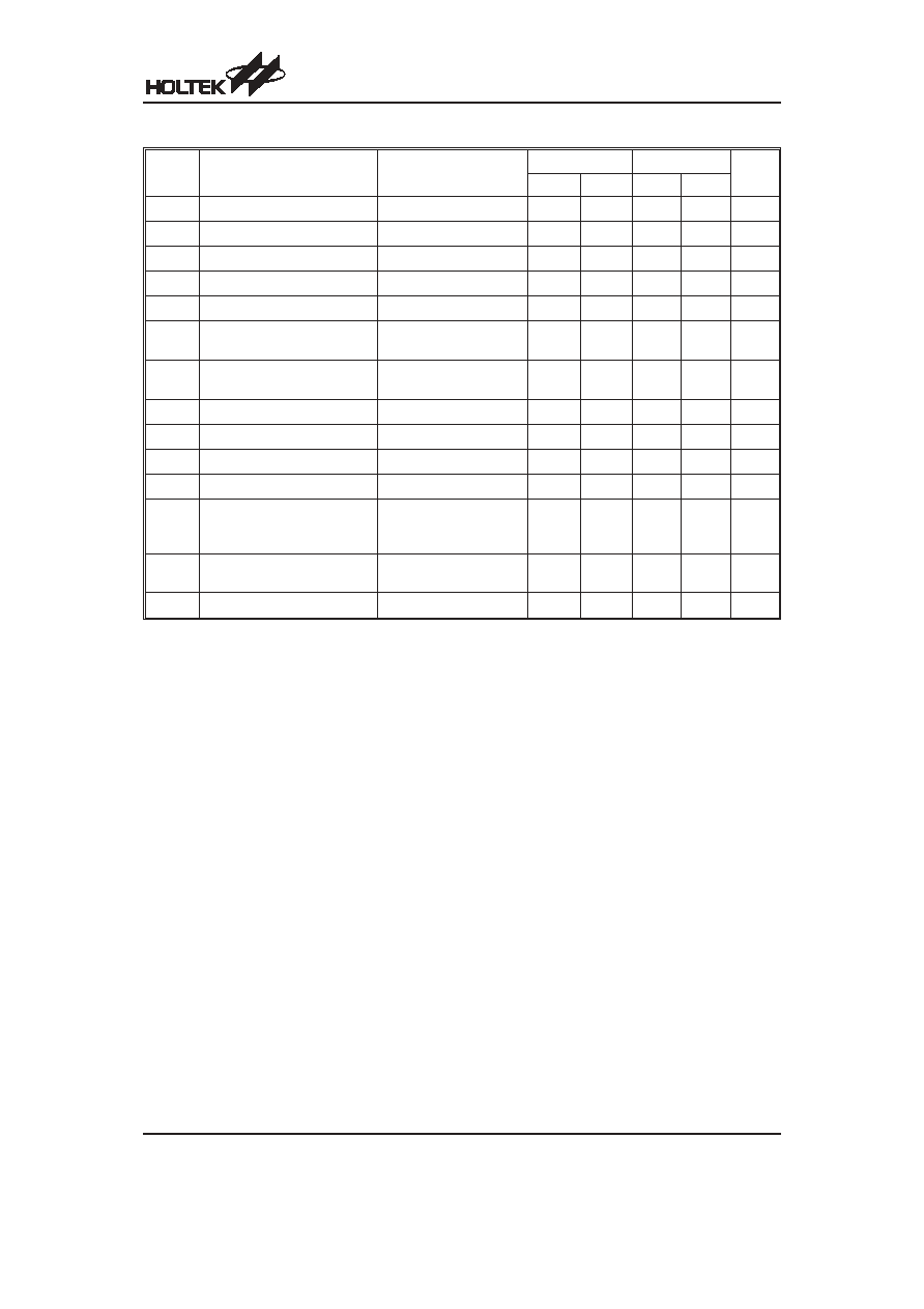
EEPROM A.C. Characteristics
Ta=25
°C
Symbol
Parameter
Remark
Standard Mode*
V
CC
=5V
±10%
Unit
Min.
Max.
Min.
Max.
f
SK
Clock Frequency
¾
¾
100
¾
400
kHz
t
HIGH
Clock High Time
¾
4000
¾
600
¾
ns
t
LOW
Clock Low Time
¾
4700
¾
1200
¾
ns
t
r
SDA and SCL Rise Time
Note
¾
1000
¾
300
ns
t
f
SDA and SCL Fall Time
Note
¾
300
¾
300
ns
t
HD:STA
START Condition Hold Time
After this period the first
clock pulse is generated
4000
¾
600
¾
ns
t
SU:STA
START Condition Setup Time
Only relevant for repeated
START condition
4000
¾
600
¾
ns
t
HD:DAT
Data Input Hold Time
¾
0
¾
0
¾
ns
t
SU:DAT
Data Input Setup Time
¾
200
¾
100
¾
ns
t
SU:STO
STOP Condition Setup Time
¾
4000
¾
600
¾
ns
t
AA
Output Valid from Clock
¾
¾
3500
¾
900
ns
t
BUF
Bus Free Time
Time in which the bus must
be free before a new trans-
mission can start
4700
¾
1200
¾
ns
t
SP
Input Filter Time Constant
(SDA and SCL Pins)
Noise suppression time
¾
100
¾
50
ns
t
WR
Write Cycle Time
¾
¾
5
¾
5
ms
Note:
These parameters are periodically sampled but not 100% tested
* The standard mode means V
CC
=2.2V to 5.5V
For relative timing, refer to timing diagrams
HT82K95EE/HT82K95AE
Rev. 1.00
5
February 15, 2006
Document Outline
- þÿ
- þÿ
- þÿ
- þÿ
- þÿ
- þÿ
- þÿ
- þÿ
- þÿ
- þÿ
- þÿ
- þÿ
- þÿ
- þÿ
- þÿ
- þÿ
- þÿ