 | ÐлекÑÑоннÑй компоненÑ: HT83006 | СкаÑаÑÑ:  PDF PDF  ZIP ZIP |
Äîêóìåíòàöèÿ è îïèñàíèÿ www.docs.chipfind.ru
HT83XXX
Q-Voice
TM
Selection Table
Body
HT83003
HT83006
HT83009
HT83018
HT83036
HT83048
HT83072
Voice ROM Size
64K-bit
128K-bit
192K-bit
384K-bit
768K-bit
1024K-bit
1536K-bit
Voice Length
3 sec
6 sec
9 sec
18 sec
36 sec
48 sec
72 sec
Rev. 0.10
1
August 25, 2003
Features
·
Operating voltage: 2.4V~5.0V
·
Up to 1
ms (0.5ms) instruction cycle with 4MHz (8MHz)
system clock
·
System clock: 4MHz~8MHz (2.4V)
·
RC oscillator for system clock
·
Eight I/O pins
·
2K
´14-bit program ROM
·
80
´8-bit RAM
·
Two 8-bit programmable timer counter with 8-stage
prescaler and one time base counter
·
Watchdog Timer
·
4-level subroutine nesting
·
HALT function and wake-up feature reduce power
consumption
·
PWM circuit direct drive speaker or output by
transistor
·
32-pin DIP package
Applications
·
Intelligent educational leisure products
·
Alert and warning systems
·
Sound effect generators
General Description
The HT83XXX series are 8-bit high performance
microcontroller with voice synthesizer and tone genera-
tor. The HT83XXX is designed for applications on multi-
ple I/Os with sound effects, such as voice and melody. It
can provide various sampling rates and beats, tone lev-
els, tempos for speech synthesizer and melody genera-
tor.
The HT83XXX is excellent for versatile voice and sound
effect product applications. The efficient MCU instruc-
tions allow users to program the powerful custom appli-
cations. The system frequency of HT83XXX can be up
to 8MHz under 2.4V and include a HALT function to re-
duce power consumption.
Preliminary
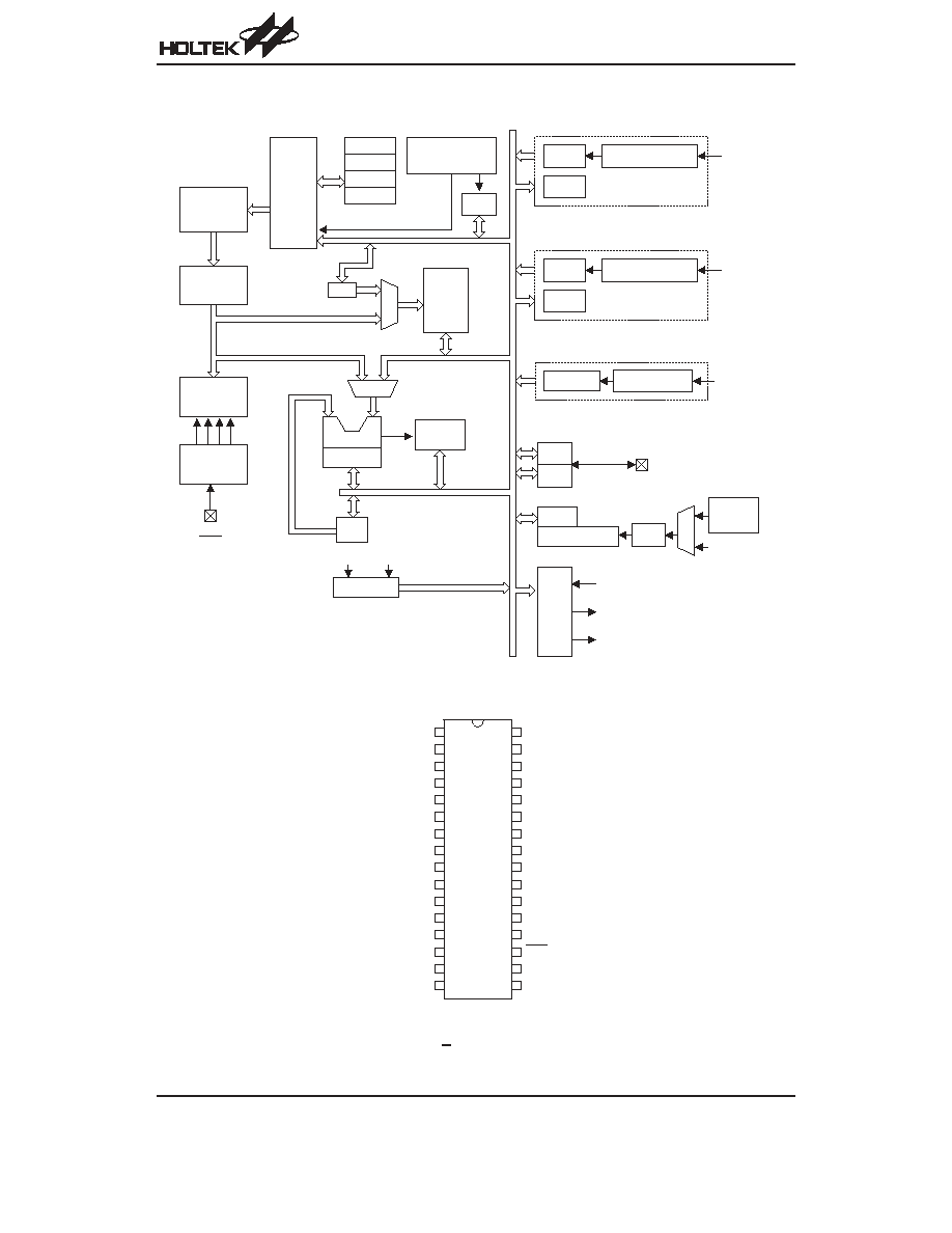
Block Diagram
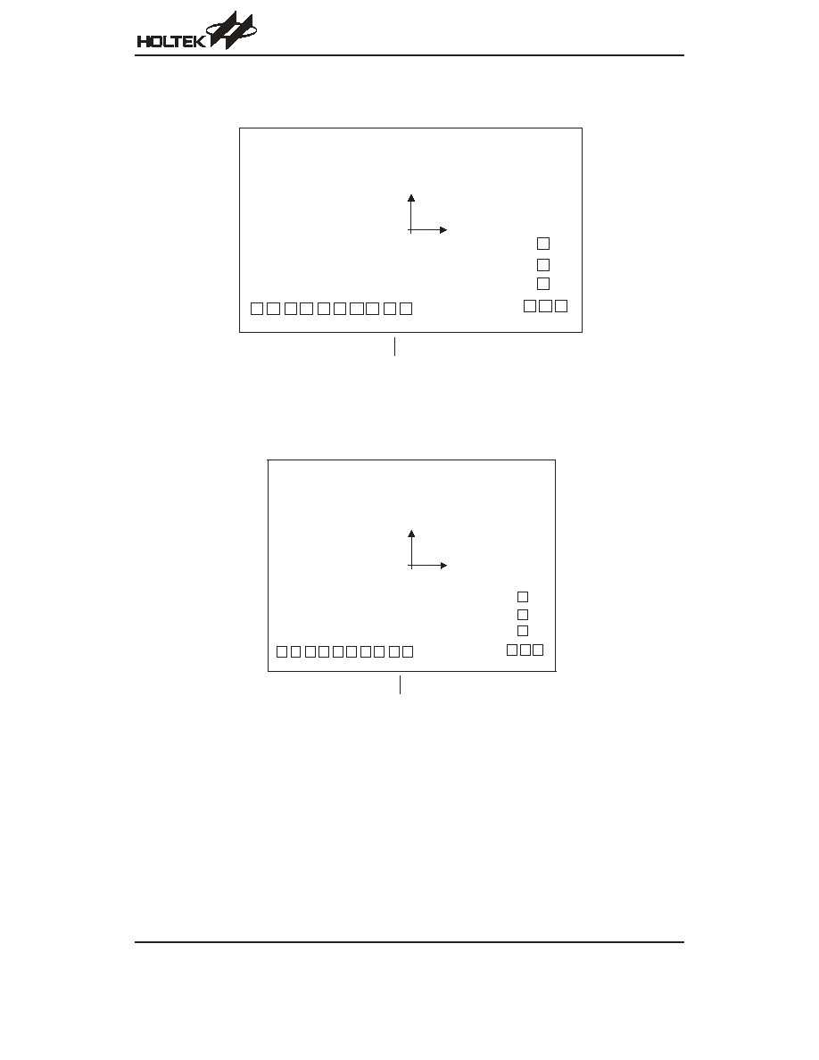
Pin Assignment
HT83XXX
Rev. 0.10
2
August 25, 2003
Preliminary
P r o g r a m
C o u n t e r
P r o g r a m
R O M
I n s t r u c t i o n
R e g i s t e r
I n s t r u c t i o n
D e c o d e r
T i m i n g
G e n e r a t i o n
O S C 1
R E S
V D D
V S S
I n t e r r u p t
C i r c u i t
I N T C
M P 0
M
U
X
M U X
D A T A
M e m o r y
A L U
S h i f t e r
S T A T U S
A C C
T M R 0
T M R 0 C
S Y S C L K
8 - b i t
L V D / L V R
P A C
P A
P O R T A
P A 0 ~ P A 7
S T A C K 2
S T A C K 3
S T A C K 0
S T A C K 1
S Y S C L K / 4
H A L T
E N / D I S
T i m e B a s e
S Y S C L K / 1 0 2 4
W D T S
W D T P r e s c a l e r
¸ 2 5 6
W D T R C
O S C
M
U
X
S Y S C L K / 4
P W M
S Y S C L K
P W M 1
P W M 2
8 - s t a g e P r e s c a l e r
T M R 1
T M R 1 C
S Y S C L K
8 - b i t
8 - s t a g e P r e s c a l e r
1
2
3
4
5
6
7
8
9
1 0
1 1
1 2
1 3
1 4
1 5
1 6
H T 8 3 0 0 3 / H T 8 3 0 0 6 / H T 8 3 0 0 9 / H T 8 3 0 1 8
H T 8 3 0 3 6 / H T 8 3 0 4 8 / H T 8 3 0 7 2
3 2 D I P - A
3 2
3 1
3 0
2 9
2 8
2 7
2 6
2 5
2 4
2 3
2 2
2 1
2 0
1 9
1 8
1 7
N C
N C
N C
N C
N C
N C
P W M 2
P W M 1
V D D A
V D D
V S S A
V S S
O S C 1
R E S
P A 7
P A 6
N C
N C
N C
N C
N C
N C
N C
N C
N C
N C
P A 0
P A 1
P A 2
P A 3
P A 4
P A 5
Pad Assignment
HT83003/HT83006/HT83009
Chip size: 2220
´ 1355 (mm)
2
* The IC substrate should be connected to VSS in the PCB layout artwork.
HT83018/HT83036
Chip size: 2220
´ 1660 (mm)
2
* The IC substrate should be connected to VSS in the PCB layout artwork.
HT83XXX
Rev. 0.10
3
August 25, 2003
Preliminary
( 0 , 0 )
2
3
4
5
6
7
8
9
1 0
1 1 1 2 1 3
1 4
1 5
1 6
1
V
D
D
V
S
S
V
S
S
A
O
S
C
1
R
E
S
P
A
7
P
A
6
P
A
5
P
A
4
P
A
3
P
A
2
P
A
1
P
A
0
P W M 2
P W M 1
V D D A
1 3
1 2
1 1
1 4
( 0 , 0 )
V
D
D
V
S
S
V
S
S
A
O
S
C
1
R
E
S
P
A
7
P
A
6
P
A
5
P
A
4
P
A
3
P
A
2
P
A
1
P
A
0
1
2
3
4
5
6
7
8
9 1 0
1 5
1 6
P W M 2
P W M 1
V D D A
HT83048/HT83072
Chip size: 2220
´ 2335 (mm)
2
* The IC substrate should be connected to VSS in the PCB layout artwork.
Pad Coordinates
HT83003/HT83006/HT83009
Pad No.
X
Y
Pad No.
X
Y
1
-982.145
-508.050
9
-135.205
-508.050
2
-876.845
-508.050
10
-31.229
-508.050
3
-766.245
-508.050
11
758.645
-490.400
4
-666.245
-508.050
12
858.645
-490.400
5
-555.645
-508.050
13
958.645
-490.400
6
-455.645
-508.050
14
841.895
-345.550
7
-345.045
-508.050
15
841.895
-224.050
8
-245.045
-508.050
16
841.895
-85.450
HT83018/HT83036
Pad No.
X
Y
Pad No.
X
Y
1
-982.145
-660.550
9
-135.205
-660.550
2
-876.845
-660.550
10
-31.229
-660.550
3
-766.245
-660.550
11
758.645
-642.900
4
-666.245
-660.550
12
858.645
-642.900
5
-555.645
-660.550
13
958.645
-642.900
6
-455.645
-660.550
14
841.895
-498.050
7
-345.045
-660.550
15
841.895
-376.550
8
-245.045
-660.550
16
841.895
-237.950
HT83XXX
Rev. 0.10
4
August 25, 2003
Preliminary
( 0 , 0 )
1
2
3
4
5
6
7
8
9
1 1 1 2 1 3
1 4
1 5
1 6
P W M 2
P W M 1
V D D A
V
D
D
V
S
S
V
S
S
A
O
S
C
1
R
E
S
P
A
7
P
A
6
P
A
5
P
A
4
P
A
3
P
A
2
P
A
1
P
A
0
HT83048/HT83072
Pad No.
X
Y
Pad No.
X
Y
1
-982.145
-998.050
9
-135.205
-998.050
2
-876.845
-998.050
10
-31.229
-998.050
3
-766.245
-998.050
11
758.645
-980.400
4
-666.245
-998.050
12
858.645
-980.400
5
-555.645
-998.050
13
958.645
-980.400
6
-455.645
-998.050
14
841.895
-835.550
7
-345.045
-998.050
15
841.895
-714.050
8
-245.045
-998.050
16
841.895
-575.450
Pad Description
Pad Name
I/O
Mask Option
Description
PA0~PA7
I/O
Wake-up,
Pull-high
or None
Bidirectional 8-bit I/O port. Each bit can be configured as a wake-up input
by mask option. Software instructions determine the CMOS output or
Schmitt trigger input with or without pull-high resistor (mask option).
VSS
¾
¾
Negative power supply, ground
VDD
¾
¾
Positive power supply
VSSA
¾
¾
PWM negative power supply, ground
VDDA
¾
¾
PWM positive power supply, ground
RES
I
¾
Schmitt trigger reset input, active low
OSC1
¾
RC
OSC1 is connected to an RC network for the internal system clock.
PWM1, PWM2
O
¾
PWM output for driving a external transistor or speaker
Absolute Maximum Ratings
Supply Voltage ..........................V
SS
+2.4V to V
SS
+5.2V
Storage Temperature ...........................
-50°C to 125°C
Input Voltage .............................V
SS
-0
.
3V to V
DD
+0.3V
Operating Temperature ..........................
-20°C to 70°C
Note: These are stress ratings only. Stresses exceeding the range specified under
²Absolute Maximum Ratings² may
cause substantial damage to the device. Functional operation of this device at other conditions beyond those
listed in the specification is not implied and prolonged exposure to extreme conditions may affect device reliabil-
ity.
D.C. Characteristics
Symbol
Parameter
Test Conditions
Min.
Typ.
Max.
Unit
V
DD
Conditions
V
DD
Operating Voltage
¾
¾
2.4
¾
5.2
V
I
STB
Standby Current
3V
No load, system HALT
¾
1
¾
mA
I
DD
Operating Current
3V
No load, f
SYS
=4MHz
¾
1.2
1.5
mA
I
OL
I/O Port Sink Current
3V
V
OL
=0.3V
17
¾
¾
mA
I
OH
I/O Port Source Current
3V
V
OH
=2.7V
-12
¾
¾
mA
I
O
PWM Source Current
3V
V
OL
=0.3V
121
¾
¾
mA
I
O
PWM Source Current
3V
V
OH
=2.7V
-81
¾
¾
mA
V
IL1
Input Low Voltage (RES)
3V
¾
¾
1.5
¾
V
V
IH1
Input High Voltage (RES)
3V
¾
¾
2.2
¾
V
f
SYS
System Frequency
3V
R
OSC
=100k
W
3.7
4.0
4.5
MHz
R
OSC
=62k
W
7.4
8.0
8.6
HT83XXX
Rev. 0.10
5
August 25, 2003
Preliminary
Document Outline
- þÿ
- þÿ
- þÿ
- þÿ
- þÿ
- þÿ
- þÿ
- þÿ
- þÿ
- þÿ
- þÿ
- þÿ
- þÿ
- þÿ
- þÿ
- þÿ