 | ÐлекÑÑоннÑй компоненÑ: HT86576 | СкаÑаÑÑ:  PDF PDF  ZIP ZIP |
Äîêóìåíòàöèÿ è îïèñàíèÿ www.docs.chipfind.ru
HT86XXX
Voice Synthesizer 8-Bit MCU
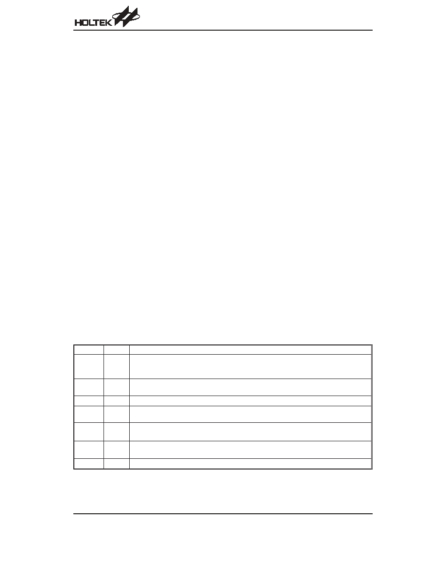
Selection Table
Body
HT86072
HT86144
HT86192
HT86384
HT86576
HT86768
Voice ROM size
1536K-bit
3072K-bit
4096K-bit
8192K-bit
12288K-bit
16392K-bit
Voice length
72 sec
144 sec
192 sec
384 sec
576 sec
768 sec
Note:
* Voice length is estimated by 21K-bit data rate
Rev. 1.70
1
May 6, 2004
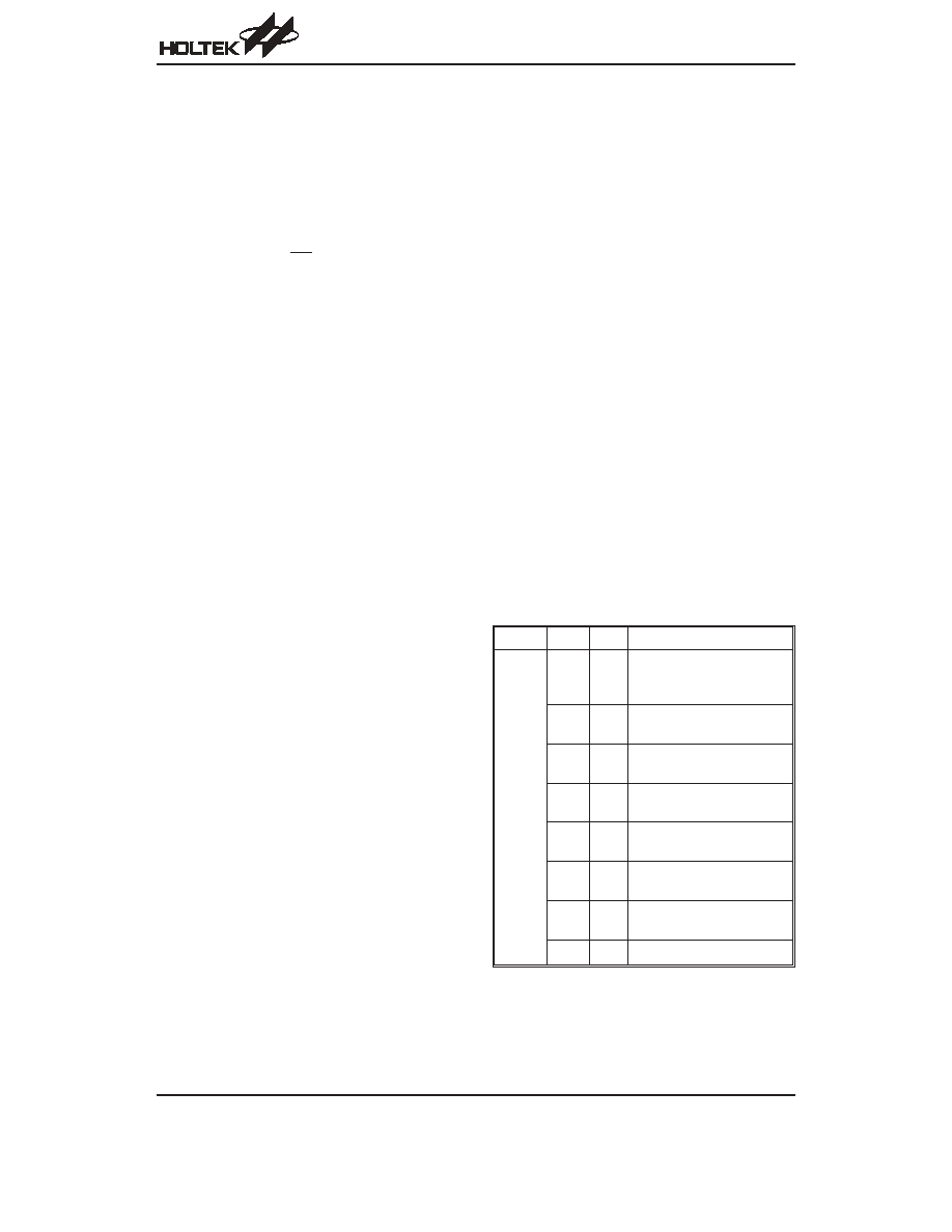
Features
·
Operating voltage: 2.4V~5.2V
·
System clock: 4MHz~8MHz
·
Crystal or RC oscillator for system clock
·
23 I/O pins with 4 shared pins included
·
8K
´16-bit program ROM
·
208
´8-bit RAM
·
One external interrupt input
·
Three 16-bit programmable timer counter and over-
flow interrupts
·
12-bit high quality D/A output by transistor or
HT82V733
·
Built-in voice ROM in various capacity
·
One optional 32768Hz crystal oscillator for RTC time
base (8-bit counter with 3-bit prescaler)
·
Watchdog Timer
·
8-level subroutine nesting
·
HALT function and wake-up feature reduce power
consumption
·
Up to 1
ms (0.5ms) instruction cycle with 4MHz (8MHz)
system clock
·
Support 16-bit table read instruction (TBLP, TBHP)
·
63 powerful and efficient instructions
·
HT86072/144/192/384: 28-pin SOP, 100-pin QFP
package
·
HT86576/768: 32-pin SOP, 100-pin QFP package
Applications
·
Intelligent educational leisure products
·
Alert and warning systems
·
High end leisure product controllers
·
Sound effect generators
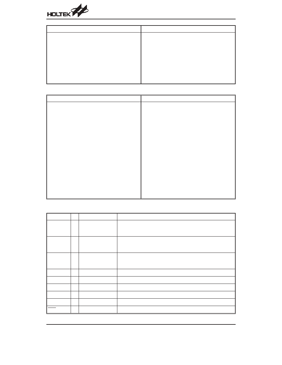
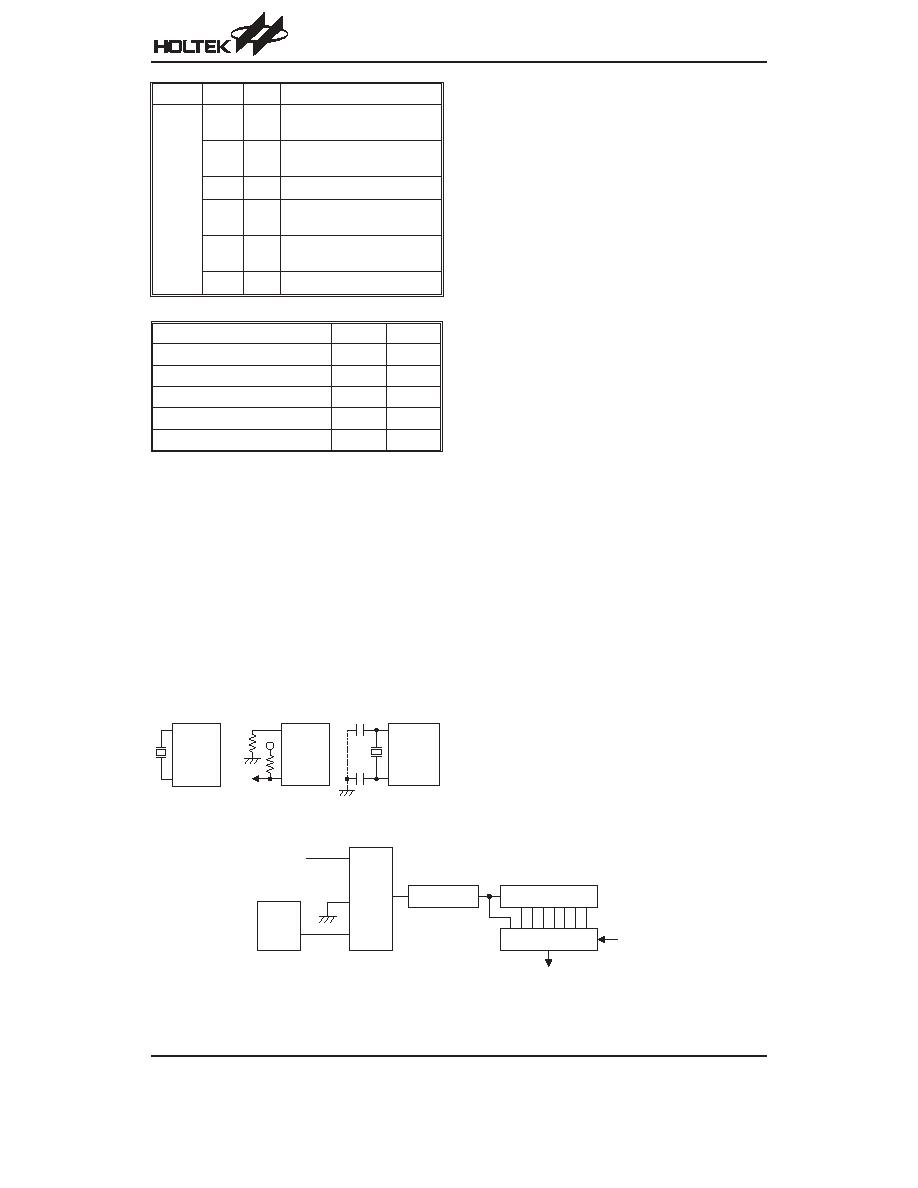
General Description
The HT86XXX series are 8-bit high performance
microcontroller with voice synthesizer and tone genera-
tor. The HT86XXX is designed for applications on multi-
ple I/Os with sound effects, such as voice and melody. It
can provide various sampling rates and beats, tone lev-
els, tempos for speech synthesizer and melody genera-
tor. It has a single built-in high quality, D/A output. There
is an external interrupt which can be triggered with fall-
ing edge pulse or falling/rising edge pulse.
The HT86XXX is excellent for versatile voice and sound
effect product applications. The efficient MCU instruc-
tions allow users to program the powerful custom appli-
cations. The system frequency of HT86XXX can be up
to 8MHz under 2.4V and include a HALT function to re-
duce power consumption.
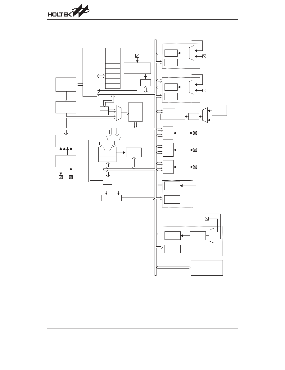
Block Diagram
HT86XXX
Rev. 1.70
2
May 6, 2004
P r o g r a m
C o u n t e r
P r o g r a m
R O M
I n s t r u c t i o n
R e g i s t e r
I n s t r u c t i o n
D e c o d e r
T i m i n g
G e n e r a t i o n
O S C 2
O S C 1
R E S
V D D
V S S
I n t e r r u p t
C i r c u i t
I N T C
M P 0
M P 1
M
U
X
M U X
D A T A
M e m o r y
A L U
S h i f t e r
S T A T U S
A C C
T M R 1
T M R 1 C
M
U
X
S Y S C L K / 4
P C 5 / T M R 1
W D T S
W D T P r e s c a l e r
¸ 2 5 6
W D T R C
O S C
1 6 b i t
T M R 0
T M R 0 C
M
U
X
S Y S C L K / 4
P C 4 / T M R 0
1 6 b i t
S T A C K 2
S T A C K 3
S T A C K 4
S T A C K 5
S T A C K 6
S T A C K 7
P C C
P C
P O R T C
P C 0 ~ P C 6
P B C
P B
P O R T B
P B 0 ~ P B 7
L V D / L V R
T M R 2
I N T
P A C
P A
P O R T A
P A 0 ~ P A 7
T M R 3 C
T M R 3
3 2 7 6 8 H z C r y s t a l
( X I N a n d X O U T )
M
U
X
S Y S C L K / 4
8 - s t a g e
P r e s c a l e r
T M R 2 C
S Y S C L K / 4
S T A C K 0
S T A C K 1
1 2 - b i t
D / A
3 - b i t
V o l u m e
C o n t r o l
M
U
X
S Y S C L K / 4
H A L T
E N / D I S
1 6 - b i t
8 - b i t
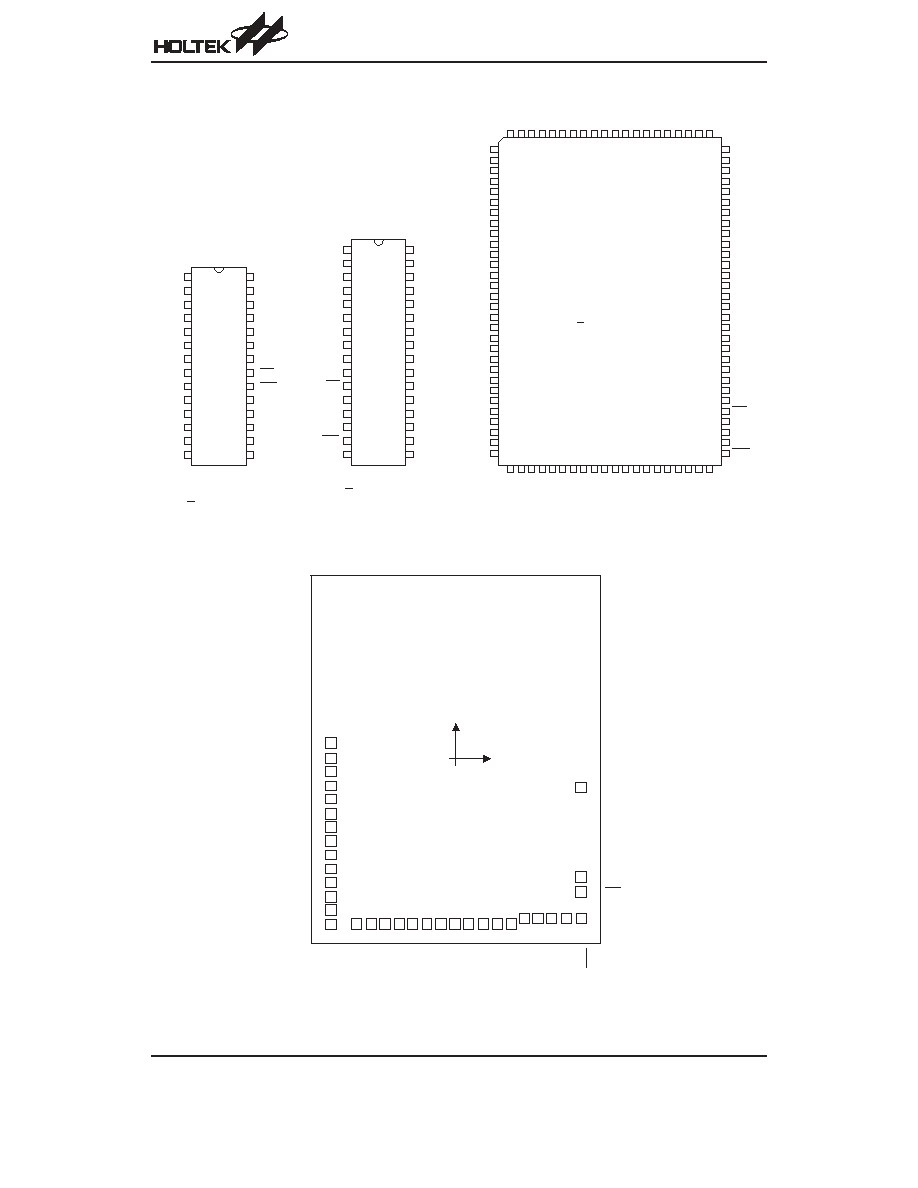
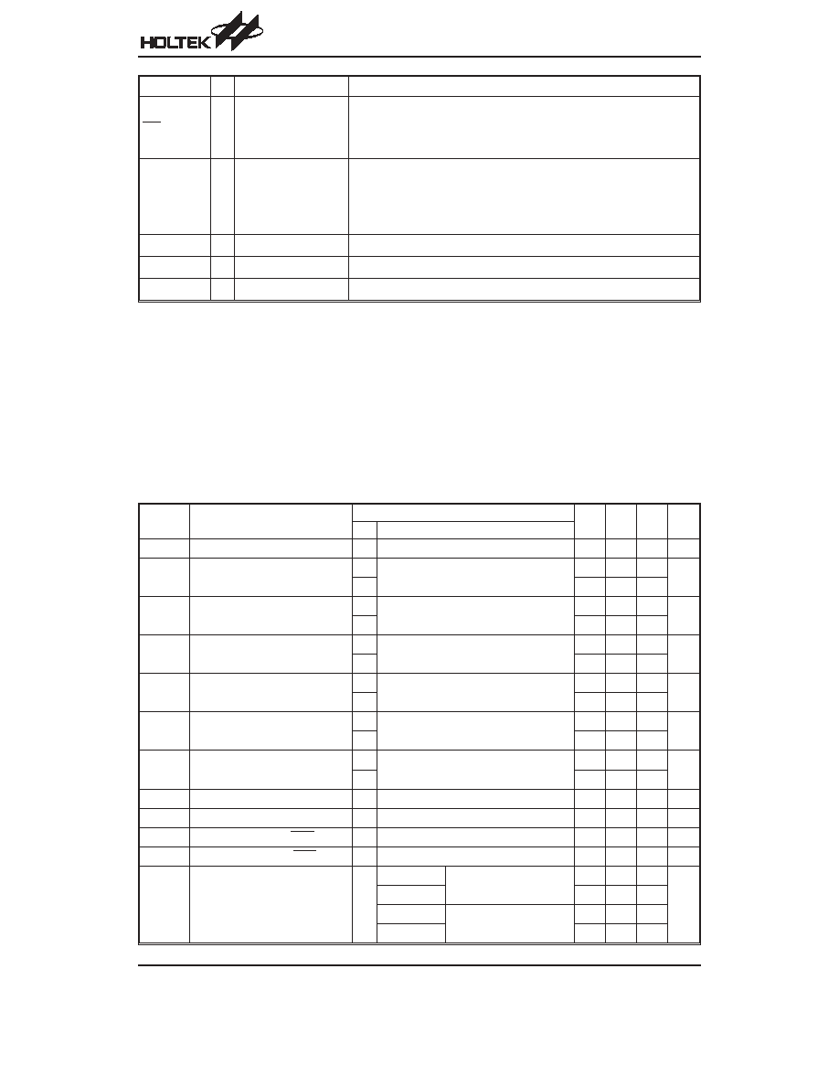
Pin Assignment
Pad Assignment
HT86072
Chip size: 2215´2830 (mm)
2
* The IC substrate should be connected to VSS in the PCB layout artwork.
HT86XXX
Rev. 1.70
3
May 6, 2004
2 8
2 7
2 6
2 5
2 4
2 3
2 2
2 1
2 0
1 9
1 8
1 7
1 6
1 5
1
2
3
4
5
6
7
8
9
1 0
1 1
1 2
1 3
1 4
H T 8 6 0 7 2 / H T 8 6 1 4 4
H T 8 6 1 9 2 / H T 8 6 3 8 4
2 8 S O P - A
N C
N C
N C
N C
P A 7
P A 6
P A 5
P A 4
P A 3
P A 2
P A 1
P A 0
N C
V S S
N C
N C
N C
N C
N C
O S C 2
O S C 1
I N T
R E S
A U D
T E S T
V D D A
V D D
V S S A
1
2
3
4
5
6
7
8
9
1 0
1 1
1 2
1 3
1 4
1 5
1 6
1 7
1 8
1 9
2 0
2 1
2 2
2 3
2 4
2 5
2 6
2 7
2 8
2 9
3 0
3 1 3 2 3 3 3 4 3 5 3 6 3 7 3 8 3 9 4 0 4 1 4 2 4 3 4 4 4 5 4 6 4 7 4 8 4 9 5 0
8 1
8 2
8 3
8 4
8 5
8 6
8 7
8 8
8 9
9 0
9 1
9 2
9 3
9 4
9 5
9 6
9 7
9 8
9 9
1 0 0
8 0
7 9
7 8
7 7
7 6
7 5
7 4
7 3
7 2
7 1
7 0
6 9
6 8
6 7
6 6
6 5
6 4
6 3
6 2
6 1
6 0
5 9
5 8
5 7
5 6
5 5
5 4
5 3
5 2
5 1
H T 8 6 0 7 2 / H T 8 6 1 4 4
H T 8 6 1 9 2 / H T 8 6 3 8 4
H T 8 6 5 7 6 / H T 8 6 7 6 8
1 0 0 Q F P - A
N C
N C
N C
N C
N C
N C
N C
N C
N C
N C
N C
N C
N C
N C
N C
N C
P A 7
P A 6
P A 5
P A 4
P A 3
P A 2
P A 1
P A 0
P B 7
N C
N C
N C
N C
P B 6
A
U
D
T
E
S
T
V
D
D
A
V
D
D
V
S
S
A
V
S
S
P
C
0
P
C
1
P
C
2
P
C
3
P
C
4
P
C
5
P
C
6
/
X
I
N
X
O
U
T
P
B
0
P
B
1
P
B
2
P
B
3
P
B
4
P
B
5
N C
N C
N C
N C
N C
N C
N C
N C
N C
N C
N C
N C
N C
N C
N C
N C
N C
N C
N C
N C
O S C 2
N C
N C
O S C 1
N C
I N T
N C
N C
N C
R E S
N
C
N
C
N
C
N
C
N
C
N
C
N
C
N
C
N
C
N
C
N
C
N
C
N
C
N
C
N
C
N
C
N
C
N
C
N
C
N
C
1
2
3
4
5
6
7
8
9
1 0
1 1
1 2
1 3
1 4
1 5
1 6
1 7
1 8
1 9
2 0
3 2
3 1
3 0
2 9
2 8
2 7
2 6
2 5
2 4
2 3
2 2
2 1
H T 8 6 5 7 6 / H T 8 6 7 6 8
3 2 S O P - B
P A 5
P A 4
P A 3
P A 2
P A 1
P A 0
N C
V S S
V D D
A U D
I N T
N C
N C
N C
R E S
O S C 1
P A 7
P A 6
N C
N C
N C
N C
N C
N C
N C
N C
N C
N C
N C
N C
N C
O S C 2
1
2
3
4
5
6
7
8
9
1 0
1 1
1 2
1 3
1 4
1 5 1 6 1 7 1 8 1 9 2 0 2 1 2 2 2 3 2 4 2 5 2 6 2 7 2 8 2 9 3 0 3 1
3 2
3 3
3 4
P A 7
P A 6
P A 5
P A 4
P A 3
P A 2
P A 1
P A 0
P B 7
P B 6
P B 5
P B 4
P B 3
P B 2
( 0 , 0 )
R
E
S
T
E
S
T
A
U
D
V
D
D
A
V
D
D
V
S
S
A
V
S
S
P
C
0
P
C
1
P
C
2
P
C
3
P
C
4
P
C
5
P
C
6
/
X
I
N
X
O
U
T
P
B
0
P
B
1
O S C 2
O S C 1
I N T
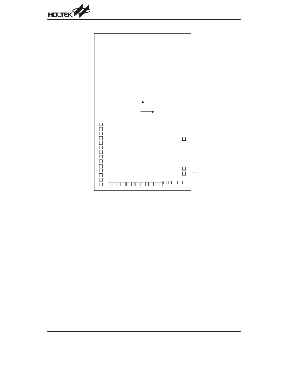
HT86144
Chip size: 2215
´3635 (mm)
2
* The IC substrate should be connected to VSS in the PCB layout artwork.
HT86XXX
Rev. 1.70
4
May 6, 2004
( 0 , 0 )
1
2
3
4
5
6
7
8
9
1 0
1 1
1 2
1 3
1 4
1 5 1 6 1 7 1 8 1 9 2 0 2 1 2 2 2 3 2 4 2 5 2 6 2 7 2 8 2 9 3 0 3 1
3 2
3 3
3 4
P A 7
P A 6
P A 5
P A 4
P A 3
P A 2
P A 1
P A 0
P B 7
P B 6
P B 5
P B 4
P B 3
P B 2
A
U
D
T
E
S
T
V
D
D
A
V
D
D
V
S
S
A
V
S
S
P
C
0
P
C
1
P
C
2
P
C
3
P
C
4
P
C
5
P
C
6
/
X
I
N
X
O
U
T
P
B
0
P
B
1
R
E
S
O S C 2
O S C 1
I N T
HT86192
Chip size: 2215
´4175 (mm)
2
* The IC substrate should be connected to VSS in the PCB layout artwork.
HT86XXX
Rev. 1.70
5
May 6, 2004
1
2
3
4
5
6
7
8
9
1 0
1 1
1 2
1 3
1 4
1 5 1 6 1 7 1 8 1 9 2 0 2 1 2 2 2 3 2 4 2 5 2 6 2 7 2 8 2 9 3 0 3 1
3 4
3 3
3 2
( 0 , 0 )
P A 7
P A 6
P A 5
P A 4
P A 3
P A 2
P A 1
P A 0
P B 7
P B 6
P B 5
P B 4
P B 3
P B 2
A
U
D
T
E
S
T
V
D
D
A
V
D
D
V
S
S
A
V
S
S
P
C
0
P
C
1
P
C
2
P
C
3
P
C
4
P
C
5
P
C
6
/
X
I
N
X
O
U
T
P
B
0
P
B
1
R
E
S
O S C 2
O S C 1
I N T
HT86384
Chip size: 2215
´6325 (mm)
2
* The IC substrate should be connected to VSS in the PCB layout artwork.
HT86XXX
Rev. 1.70
6
May 6, 2004
P A 7
P A 6
P A 5
P A 4
P A 3
P A 2
P A 1
P A 0
P B 7
P B 6
P B 5
P B 4
P B 3
P B 2
A
U
D
T
E
S
T
V
D
D
A
V
D
D
V
S
S
A
V
S
S
P
C
0
P
C
1
P
C
2
P
C
3
P
C
4
P
C
5
P
C
6
/
X
I
N
X
O
U
T
P
B
0
P
B
1
R
E
S
O S C 2
O S C 1
I N T
( 0 , 0 )
1
2
3
4
5
6
7
8
9
1 0
1 1
1 2
1 3
1 4
1 5 1 6 1 7 1 8 1 9 2 0 2 1 2 2 2 3 2 4 2 5 2 6 2 7 2 8 2 9 3 0 3 1
3 4
3 3
3 2
HT86576
Chip size: 4060
´4740 (mm)
2
* The IC substrate should be connected to VSS in the PCB layout artwork.
HT86XXX
Rev. 1.70
7
May 6, 2004
( 0 , 0 )
1
2
3
4
5
6
7
8
9
1 0 1 1 1 2 1 3 1 4 1 5 1 6 1 7 1 8 1 9 2 0
2 1 2 2 2 3 2 4 2 5 2 6 2 7 2 8 2 9 3 0 3 1 3 2
3 3
3 4
P A 7
P A 6
P A 5
P A 4
P A 3
P A 2
P A 1
P A 0
P B 7
I
N
T
R
E
S
A
U
D
T
E
S
T
V
D
D
A
V
D
D
V
S
S
A
V
S
S
P
C
0
P
C
1
P
C
2
P
C
3
O S C 2
O S C 1
P
C
4
P
C
5
P
C
6
/
X
I
N
X
O
U
T
P
B
0
P
B
1
P
B
2
P
B
3
P
B
4
P
B
5
P
B
6
HT86768
Chip size: 4060
´5805 (mm)
2
* The IC substrate should be connected to VSS in the PCB layout artwork.
HT86XXX
Rev. 1.70
8
May 6, 2004
( 0 , 0 )
1
2
3
4
5
6
7
8
9
1 0 1 1 1 2 1 3 1 4 1 5 1 6 1 7 1 8 1 9 2 0
2 1 2 2 2 3 2 4 2 5 2 6 2 7 2 8 2 9 3 0 3 1 3 2
3 3
3 4
P A 7
P A 6
P A 5
P A 4
P A 3
P A 2
P A 1
P A 0
P B 7
P
C
4
P
C
5
P
C
6
/
X
I
N
X
O
U
T
P
B
0
P
B
1
P
B
2
P
B
3
P
B
4
P
B
5
P
B
6
O S C 2
O S C 1
I
N
T
R
E
S
A
U
D
T
E
S
T
V
D
D
A
V
D
D
V
S
S
A
V
S
S
P
C
0
P
C
1
P
C
2
P
C
3

Pad Coordinates
HT86072
Pad No.
X
Y
Pad No.
X
Y
1
-942.295
118.250
18
-425.400
-1249.300
2
-942.295
7.650
19
-325.400
-1249.300
3
-942.295
-92.350
20
-214.800
-1249.300
4
-942.295
-202.950
21
-114.800
-1249.300
5
-942.295
-302.950
22
-4.200
-1249.300
6
-942.295
-413.550
23
95.800
-1249.300
7
-942.295
-513.550
24
206.400
-1249.300
8
-942.295
-624.150
25
316.215
-1249.350
9
-942.295
-724.150
26
416.415
-1249.350
10
-942.295
-834.750
27
516.415
-1212.300
11
-942.295
-934.750
28
616.415
-1212.300
12
-942.295
-1045.350
29
721.415
-1212.300
13
-942.295
-1145.350
30
833.215
-1212.300
14
-942.295
-1255.950
31
946.426
-1212.300
15
-746.600
-1249.300
32
940.115
-1007.289
16
-636.000
-1249.300
33
940.065
-891.826
17
-536.000
-1249.300
34
940.065
-213.974
HT86144
Pad No.
X
Y
Pad No.
X
Y
1
-942.295
-284.211
18
-425.400
-1651.761
2
-942.295
-394.811
19
-325.400
-1651.761
3
-942.295
-494.811
20
-214.800
-1651.761
4
-942.295
-605.411
21
-114.800
-1651.761
5
-942.295
-705.411
22
-4.200
-1651.761
6
-942.295
-816.011
23
95.800
-1651.761
7
-942.295
-916.011
24
206.400
-1651.761
8
-942.295
-1026.611
25
316.215
-1651.811
9
-942.295
-1126.611
26
416.415
-1651.811
10
-942.295
-1237.211
27
516.415
-1614.761
11
-942.295
-1337.211
28
616.415
-1614.761
12
-942.295
-1447.811
29
721.415
-1614.761
13
-942.295
-1547.811
30
833.215
-1614.761
14
-942.295
-1658.411
31
946.426
-1614.761
15
-746.600
-1651.761
32
940.115
-1409.750
16
-636.000
-1651.761
33
940.065
-1294.287
17
-536.000
-1651.761
34
940.065
-616.435
HT86XXX
Rev. 1.70
9
May 6, 2004

HT86192
Pad No.
X
Y
Pad No.
X
Y
1
-942.295
-553.325
18
-425.400
-1920.875
2
-942.295
-663.925
19
-325.400
-1920.875
3
-942.295
-763.925
20
-214.800
-1920.875
4
-942.295
-874.525
21
-114.800
-1920.875
5
-942.295
-974.525
22
-4.200
-1920.875
6
-942.295
-1085.125
23
95.800
-1920.875
7
-942.295
-1185.125
24
206.400
-1920.875
8
-942.295
-1295.725
25
316.215
-1920.925
9
-942.295
-1395.725
26
416.415
-1920.925
10
-942.295
-1506.325
27
516.415
-1883.875
11
-942.295
-1606.325
28
616.415
-1883.875
12
-942.295
-1716.925
29
721.415
-1883.875
13
-942.295
-1816.925
30
833.215
-1883.875
14
-942.295
-1927.525
31
946.426
-1883.875
15
-746.600
-1920.875
32
940.115
-1678.864
16
-636.000
-1920.875
33
940.065
-1563.401
17
-536.000
-1920.875
34
940.065
-885.549
HT86384
Pad No.
X
Y
Pad No.
X
Y
1
-942.295
-1627.476
18
-425.400
-2995.026
2
-942.295
-1738.076
19
-325.400
-2995.026
3
-942.295
-1838.076
20
-214.800
-2995.026
4
-942.295
-1948.676
21
-114.800
-2995.026
5
-942.295
-2048.676
22
-4.200
-2995.026
6
-942.295
-2159.276
23
95.800
-2995.026
7
-942.295
-2259.276
24
206.400
-2995.026
8
-942.295
-2369.876
25
316.215
-2995.076
9
-942.295
-2469.876
26
416.415
-2995.076
10
-942.295
-2580.476
27
516.415
-2958.026
11
-942.295
-2680.476
28
616.415
-2958.026
12
-942.295
-2791.076
29
721.415
-2958.026
13
-942.295
-2891.076
30
833.215
-2958.026
14
-942.295
-3001.676
31
946.426
-2958.026
15
-746.600
-2995.026
32
940.115
-2753.015
16
-636.000
-2995.026
33
940.065
-2637.552
17
-536.000
-2995.026
34
940.065
-1959.700
HT86576
Pad No.
X
Y
Pad No.
X
Y
1
-1864.850
-1331.600
18
-764.350
-2204.850
2
-1864.850
-1442.200
19
-663.350
-2204.850
3
-1864.850
-1542.200
20
-552.750
-2204.850
4
-1864.850
-1652.800
21
659.200
-2204.850
5
-1864.850
-1752.800
22
769.800
-2204.850
6
-1864.850
-1863.400
23
869.800
-2204.850
7
-1864.850
-1963.400
24
980.400
-2204.850
8
-1864.850
-2074.000
25
1110.300
-2204.900
HT86XXX
Rev. 1.70
10
May 6, 2004
Pad No.
X
Y
Pad No.
X
Y
9
-1864.850
-2174.000
26
1210.500
-2204.900
10
-1618.550
-2204.850
27
1310.510
-2167.850
11
-1518.550
-2204.850
28
1425.500
-2167.850
12
-1407.950
-2204.850
29
1530.500
-2167.850
13
-1307.950
-2204.850
30
1642.300
-2167.850
14
-1197.350
-2204.850
31
1755.511
-2167.850
15
-1097.350
-2204.850
32
1860.559
-2167.850
16
-986.750
-2204.850
33
1859.150
-1935.526
17
-881.025
-2204.850
34
1859.150
-1257.674
HT86768
Pad No.
X
Y
Pad No.
X
Y
1
-1864.850
-1864.100
18
-764.350
-2737.350
2
-1864.850
-1974.700
19
-663.350
-2737.350
3
-1864.850
-2074.700
20
-552.750
-2737.350
4
-1864.850
-2185.300
21
659.200
-2737.350
5
-1864.850
-2285.300
22
769.800
-2737.350
6
-1864.850
-2395.900
23
869.800
-2737.350
7
-1864.850
-2495.900
24
980.400
-2737.350
8
-1864.850
-2606.500
25
1110.300
-2737.400
9
-1864.850
-2706.500
26
1210.500
-2737.400
10
-1618.550
-2737.350
27
1310.510
-2700.350
11
-1518.550
-2737.350
28
1425.500
-2700.350
12
-1407.950
-2737.350
29
1530.500
-2700.350
13
-1307.950
-2737.350
30
1642.300
-2700.350
14
-1197.350
-2737.350
31
1755.511
-2700.350
15
-1097.350
-2737.350
32
1860.559
-2700.350
16
-986.750
-2737.350
33
1859.150
-2468.026
17
-881.025
-2737.350
34
1859.150
-1790.174
Pad Description
Pad Name
I/O
Mask Option
Description
PA0~PA7
I/O
Wake-up,
Pull-high
or None
Bidirectional 8-bit I/O port. Each bit can be configured as a wake-up input
by mask option. Software instructions determine the CMOS output or
Schmitt trigger input with or without pull-high resistor (mask option).
PB0~PB7
I/O
Pull-high
or None
Bidirectional 8-bit I/O port. Software instructions determine the CMOS
output or Schmitt trigger input (pull-high resistor depending on mask op-
tion).
PC0~PC5
PC6/XIN
I/O
Pull-high
or None
Bidirectional 7-bit I/O port. Software instructions determine the CMOS
output or Schmitt trigger input (pull-high resistor depending on mask op-
tion). XIN is pin-shared with PC6
XOUT
¾
32kHz RTC
Connected an external 32kHz crystal to XIN and XOUT.
VSS
¾
¾
Negative power supply, ground
VDD
¾
¾
Positive power supply
VDDA
¾
¾
DAC power supply
VSSA
¾
¾
DAC negative power supply, ground
RES
I
¾
Schmitt trigger reset input, active low
HT86XXX
Rev. 1.70
11
May 6, 2004
Pad Name
I/O
Mask Option
Description
INT
I
Falling Edge Trigger
or Falling/Rising Edge
Trigger
External interrupt Schmitt trigger input without pull-high resistor. Choice
falling edge trigger or falling/rising edge trigger by mask option. Falling
edge triggered active on a high to low transition. Rising edge triggered
active on a low to high transition.
OSC1
OSC2
¾
RC or Crystal
OSC1 and OSC2 are connected to an RC network or a crystal (by mask
option) for the internal system clock. In the case of RC operation, OSC2
is the output terminal for 1/4 system clock.
The system clock may come from the crystal, the two pins cannot be
floating.
AUD
O
¾
Audio output for driving a external transistor or for driving HT82V733
NC
¾
¾
No connection
TEST
¾
¾
No connection (open)
Absolute Maximum Ratings
Supply Voltage ..........................V
SS
-0.3V to V
SS
+5.5V
Storage Temperature ...........................
-50°C to 125°C
Input Voltage .............................V
SS
-0
.
3V to V
DD
+0.3V
Operating Temperature ..........................
-20°C to 70°C
Note: These are stress ratings only. Stresses exceeding the range specified under
²Absolute Maximum Ratings² may
cause substantial damage to the device. Functional operation of this device at other conditions beyond those
listed in the specification is not implied and prolonged exposure to extreme conditions may affect device reliabil-
ity.
D.C. Characteristics
Ta=25
°C
Symbol
Parameter
Test Conditions
Min. Typ. Max. Unit
V
DD
Conditions
V
DD
Operating Voltage
¾ f
SYS
=4MHz/8MHz
2.4
¾
5.2
V
I
STB1
Standby Current (Watchdog Off)
3V
No load, system HALT
¾
¾
1
mA
5V
¾
¾
2
I
STB2
Standby Current(Watchdog On)
3V
No load, system HALT
¾
¾
7
mA
5V
¾
¾
10
I
DD
Operating Current (Crystal OSC)
3V
No load, f
SYS
=4MHz
¾
¾
3
mA
5V
¾
¾
7
I
OL
I/O Port Sink Current
3V
V
OL
=0.1V
DD
¾
4
¾
mA
5V
¾
10
¾
I
OH
I/O Port Source Current
3V
V
OH
=0.9V
DD
¾
-2
¾
mA
5V
¾
-5
¾
I
O
AUD Source Current
3V
V
OH
=0.9V
DD
¾
-3
¾
mA
5V
¾
-6
¾
V
IL1
Input Low Voltage for I/O Ports
3V
¾
¾
1.3
¾
V
V
IH1
Input High Voltage for I/O Ports
3V
¾
¾
1.8
¾
V
V
IL2
Reset Low Voltage (RES)
3V
¾
¾
1.5
¾
V
V
IH2
Reset High Voltage (RES)
3V
¾
¾
2.4
¾
V
f
SYS
System Frequency
3V
R
OSC
=100k
W For HT86072, HT86144,
HT86192, HT86384 only
¾
4.0
¾
MHz
R
OSC
=62k
W
¾
8.0
¾
R
OSC
=240k
W For HT86576, HT86768
only
¾
4.0
¾
R
OSC
=150k
W
¾
8.0
¾
HT86XXX
Rev. 1.70
12
May 6, 2004
Symbol
Parameter
Test Conditions
Min. Typ. Max. Unit
V
DD
Conditions
R
PH
Pull-high Resistance
3V
¾
20
60
100
k
W
5V
10
30
50
A.C. Characteristics
Ta=25
°C
Symbol
Parameter
Test Conditions
Min. Typ. Max. Unit
V
DD
Conditions
f
SYS1
System Clock (RC OSC)
¾ 2.4V~5.2V
4
¾
8
MHz
f
SYS2
System Clock (Crystal OSC)
¾ 2.4V~5.2V
4
¾
8
MHz
f
TIMER
Timer Input Frequency
¾ 2.4V~5.2V
0
¾
8
MHz
t
WDTOSC
Watchdog Oscillator Period
3V
¾
45
90
180
ms
5V
¾
32
65
130
ms
t
WDT1
W a t c h d o g T i m e - o u t P e r i o d
(WDT OSC)
3V
Without WDT prescaler
11
23
46
ms
5V
8
17
33
ms
t
WDT2
Watchdog Time-out Period (Sys-
tem Clock)
¾ Without WDT prescaler
¾ 1024 ¾
t
SYS
t
WDT3
Watchdog Time-out Period (RTC
OSC)
¾ Without WDT prescaler
¾ 7.812 ¾
ms
t
RES
External Reset Low Pulse Width
¾
¾
1
¾
¾
ms
t
SST
System Start-up Timer Period
¾ Wake-up from HALT
¾ 1024 ¾
t
SYS
t
INT
Interrupt Pulse Width
¾
¾
1
¾
¾
ms
Characteristics Curves
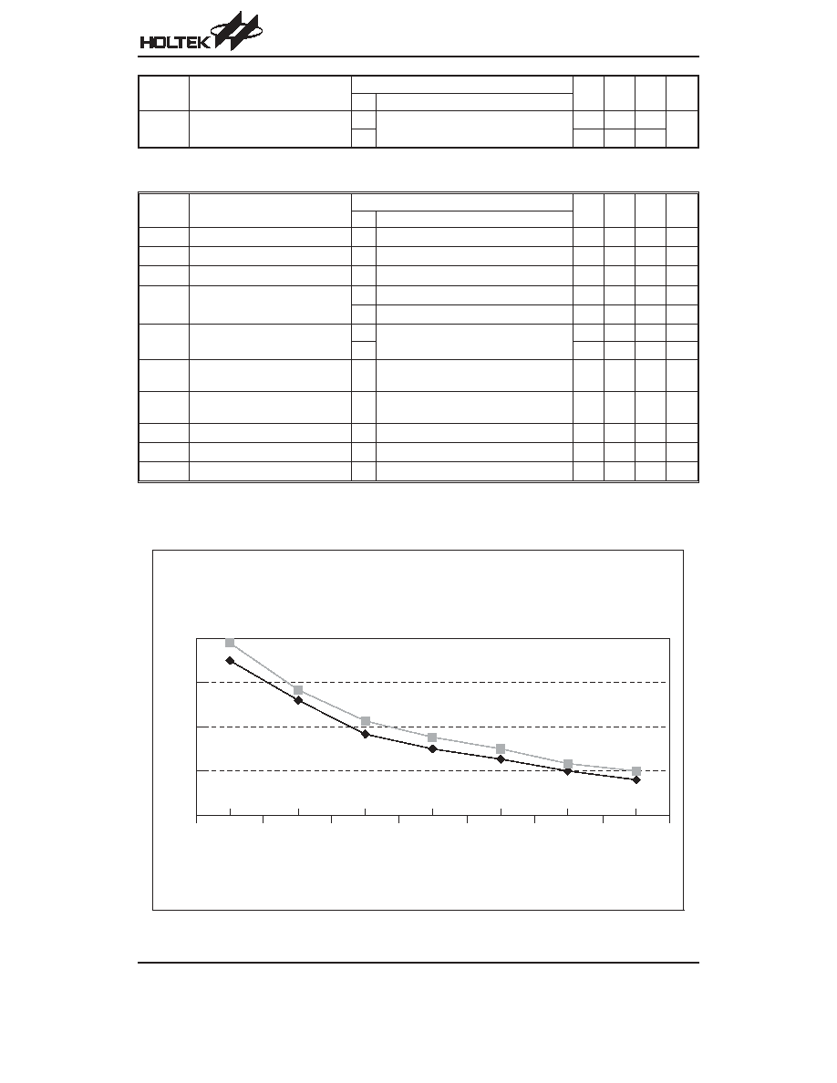
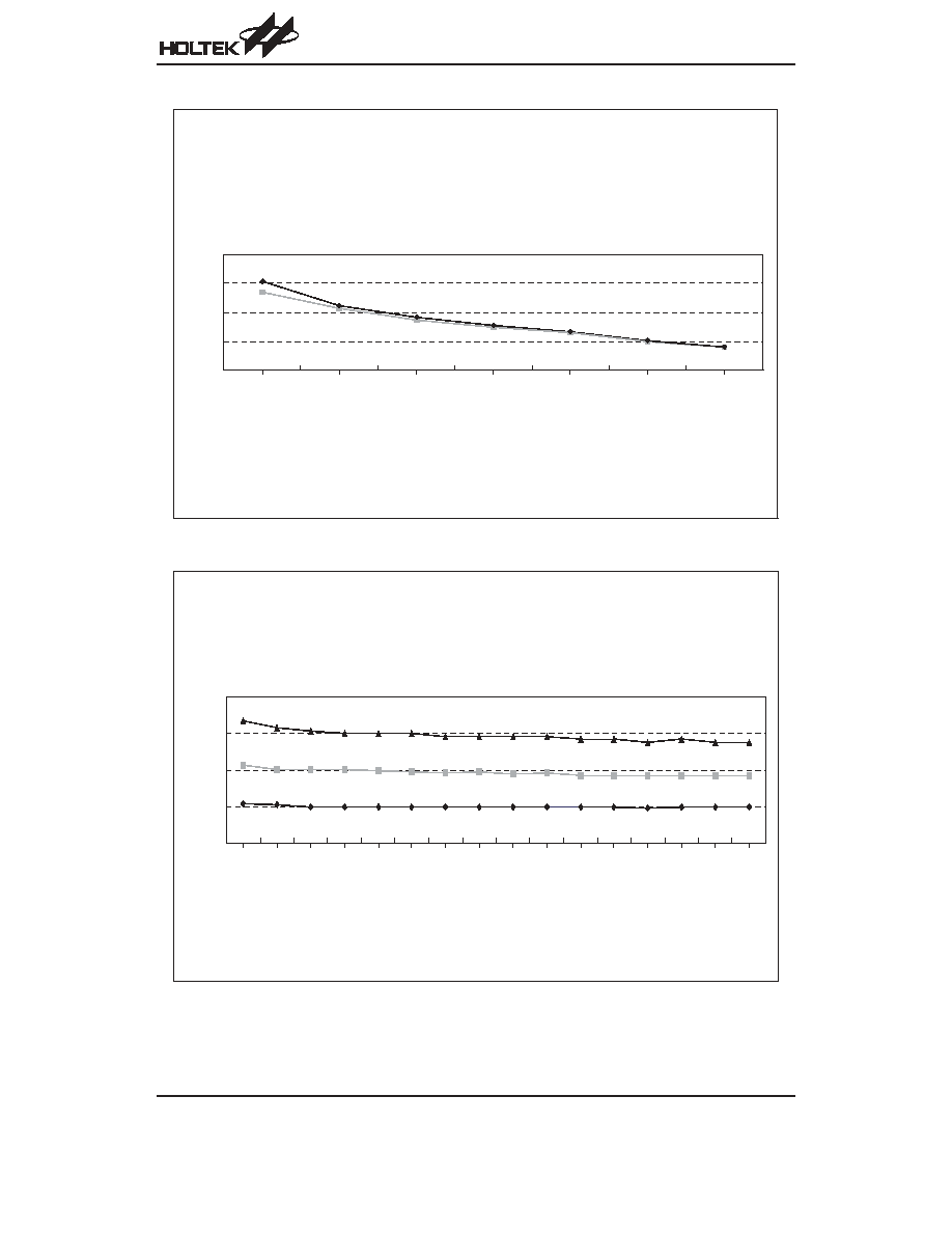
HT86072/HT86144/HT86192/HT86384 R vs. F Characteristics Curve
HT86XXX
Rev. 1.70
13
May 6, 2004
H T 8 6 0 7 2 / H T 8 6 1 4 4 / H T 8 6 1 9 2 / H T 8 6 3 8 4 R v s . F C h a r t
F
r
e
q
u
e
n
c
y
(
M
H
z
)
1 0
8
6
4
2
R ( k W )
4 . 5 V
3 . 0 V
1 1 5
1 0 5
9 5
8 5
7 5
6 5
5 5
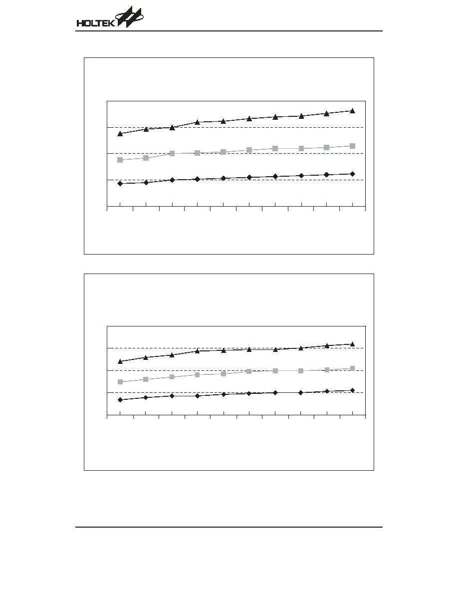
HT86072/HT86144/HT86192/HT86384 V vs. F Characteristics Curve
HT86XXX
Rev. 1.70
14
May 6, 2004
H T 8 6 0 7 2 / H T 8 6 1 4 4 / H T 8 6 1 9 2 / H T 8 6 3 8 4 V v s . F C h a r t ( F o r 3 . 0 V )
V
D D
( V )
F
r
e
q
u
e
n
c
y
(
M
H
z
)
1 0
8
6
4
2
2 . 4
2 . 7
3
3 . 3
3 . 6
3 . 9
4 . 2
4 . 8
5 . 2
H T 8 6 0 7 2 / H T 8 6 1 4 4 / H T 8 6 1 9 2 / H T 8 6 3 8 4 V v s . F C h a r t ( F o r 4 . 5 V )
V
D D
( V )
F
r
e
q
u
e
n
c
y
(
M
H
z
)
1 0
8
6
4
2
4 . 5
8 M H z / 6 2 k W
6 M H z / 7 7 k W
4 M H z / 1 0 5 k W
2 . 4
2 . 7
3
3 . 3
3 . 6
3 . 9
4 . 2
4 . 8
5 . 2
4 . 5
8 M H z / 6 9 k W
6 M H z / 8 4 k W
4 M H z / 1 1 5 k W
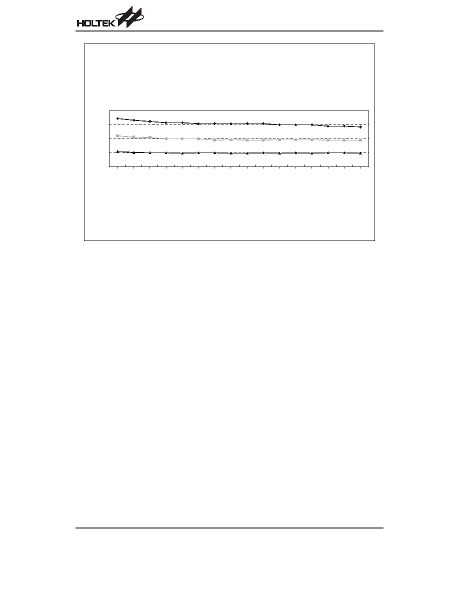
HT86576/HT86768 R vs. F Characteristics Curve
HT86576/HT86768 V vs. F Characteristics Curve
HT86XXX
Rev. 1.70
15
May 6, 2004
H T 8 6 5 7 6 / H T 8 6 7 6 8 R v s . F C h a r t
R ( k W )
F
r
e
q
u
e
n
c
y
(
M
H
z
)
1 5 0
1 8 0
2 0 0
2 2 0
2 4 0
2 7 0
3 0 0
1 0
8
6
4
2
3 . 0 V
4 . 5 V
H T 8 6 5 7 6 / H T 8 6 7 6 8 V v s . F C h a r t ( F o r 3 . 0 V )
V
D D
( V )
F
r
e
q
u
e
n
c
y
(
M
H
z
)
1 0
8
6
4
2
2 . 4
2 . 6
2 . 8
3
3 . 2
3 . 4
3 . 6
3 . 8
4
4 . 2
4 . 4
4 . 6
4 . 8
5
5 . 2
8 M H z / 1 5 5 k W
4 M H z / 2 7 9 k W
6 M H z / 1 9 3 k W
4 . 5
HT86XXX
Rev. 1.70
16
May 6, 2004
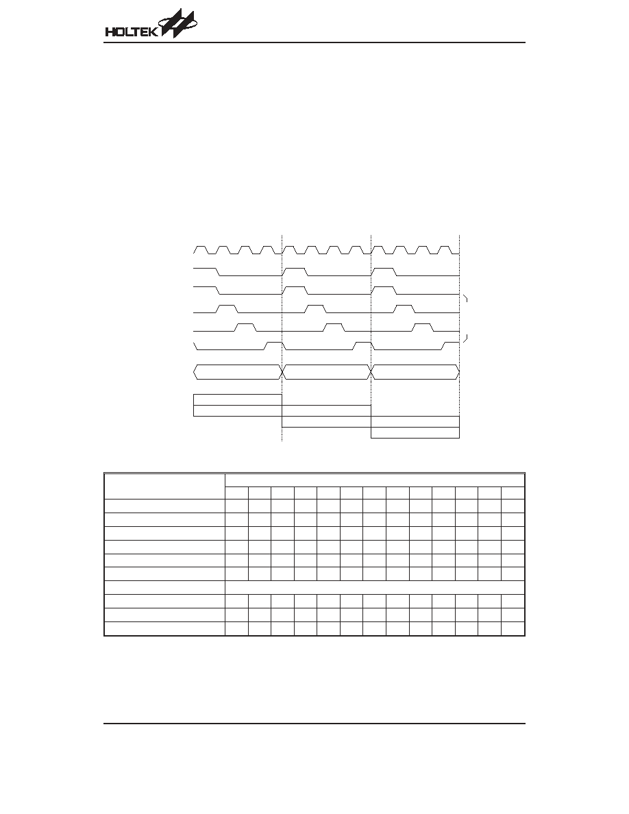
H T 8 6 5 7 6 / H T 8 6 7 6 8 V v s . F C h a r t ( F o r 4 . 5 V )
V
D D
( V )
F
r
e
q
u
e
n
c
y
(
M
H
z
)
1 0
8
6
4
2
2 . 4
2 . 6
2 . 8
3
3 . 2
3 . 4
3 . 6
3 . 8
4
4 . 2
4 . 4
4 . 6
4 . 8
5
5 . 2
4 . 5
8 M H z / 1 4 7 k W
4 M H z / 2 7 5 k W
6 M H z / 1 9 2 k W
HT86XXX
Rev. 1.70
17
May 6, 2004
Functional Description
Execution Flow
The system clock for the HT86XXX series is derived
from either a crystal or an RC oscillator. It is internally di-
vided into four non-overlapping clocks. One instruction
cycle consists of four system clock cycles.
Instruction fetching and execution are pipelined in such
a way that a fetch takes one instruction cycle while de-
coding and execution takes the next instruction cycle.
However, the pipelining scheme causes each instruc-
tion to effectively execute within one cycle. If an instruc-
tion changes the program counter, two cycles are
required to complete the instruction.
Program Counter
- PC
The 13-bit program counter (PC) controls the sequence
in which the instructions stored in program ROM are ex-
ecuted.
After accessing a program memory word to fetch an in-
struction code, the contents of the program counter are
incremented by one. The program counter then points
to the memory word containing the next instruction
code.
When executing a jump instruction, conditional skip ex-
ecution, loading PCL register, subroutine call, initial re-
set, internal interrupt, external interrupt or return from
Mode
Program Counter
*12
*11
*10
*9
*8
*7
*6
*5
*4
*3
*2
*1
*0
Initial Reset
0
0
0
0
0
0
0
0
0
0
0
0
0
External or Serial Input Interrupt
0
0
0
0
0
0
0
0
0
0
1
0
0
Timer/Event Counter 0 Overflow
0
0
0
0
0
0
0
0
0
1
0
0
0
Timer/Event Counter 1 Overflow
0
0
0
0
0
0
0
0
0
1
1
0
0
Timer Counter 2 Overflow
0
0
0
0
0
0
0
0
1
0
0
0
0
Timer Counter 3 Overflow
0
0
0
0
0
0
0
0
1
0
1
0
0
Skip
PC+2
Loading PCL
*12
*11
*10
*9
*8
@7
@6
@5
@4
@3
@2
@1
@0
Jump, Call Branch
#12
#11
#10
#9
#8
#7
#6
#5
#4
#3
#2
#1
#0
Return from Subroutine
S12
S11
S10
S9
S8
S7
S6
S5
S4
S3
S2
S1
S0
Program Counter
Note: *12~*0: Program counter bits
S12~S0: Stack register bits
#12~#0: Instruction code bits
@7~@0: PCL bits
T 1
T 2
T 3
T 4
T 1
T 2
T 3
T 4
T 1
T 2
T 3
T 4
F e t c h I N S T ( P C )
E x e c u t e I N S T ( P C - 1 )
F e t c h I N S T ( P C + 1 )
E x e c u t e I N S T ( P C )
F e t c h I N S T ( P C + 2 )
E x e c u t e I N S T ( P C + 1 )
P C
P C + 1
P C + 2
S y s t e m C l o c k
O S C ( R C o n l y )
P C
P 1
P 2
P 3
P 4
I n t e r n a l
P h a s e
C l o c k s
Execution Flow
HT86XXX
Rev. 1.70
18
May 6, 2004
subroutine, the PC manipulates the program transfer by
loading the address corresponding to each instruction.
The conditional skip is activated by instruction. Once the
condition is met, the next instruction, fetched during the
current instruction execution, is discarded and a dummy
cycle takes its place while the correct instruction is ob-
tained.
The lower byte of the program counter (PCL) is a
read/write register (06H). Moving data into the PCL per-
forms a short jump. The destination must be within 256
locations.
When a control transfer takes place, an additional
dummy cycle is required.
Program Memory
- ROM
The program memory stores the program instructions
that are to be executed. It also includes data, table and
interrupt entries, addressed by the program counter
along with the table pointer. The program memory size
for HT86XXX is 8192
´16 bits. Certain locations in the
program memory are reserved for special usage:
·
Location 000H
This area is reserved for program initialization. The
program always begins execution at location 000H
each time the system is reset.
·
Location 004H
This area is reserved for the external interrupt service
program. If the INT input pin is activated, and the inter-
rupt is enabled and the stack is not full, the program
will jump to location 004H and begins execution.
·
Location 008H
This area is reserved for the 16-bit Timer/Event Coun-
ter 0 interrupt service program. If a timer interrupt re-
sults from a Timer/Event Counter 0 overflow, and if the
interrupt is enabled and the stack is not full, the pro-
gram will jump to location 008H and begins execution.
·
Location 00CH
This area is reserved for the 16-bit Timer/Event Coun-
ter 1 interrupt service program. If a timer interrupt re-
sults from a Timer/Event Counter 1 overflow, and if the
interrupt is enabled and the stack is not full, the pro-
gram will jump to location 00CH and begins execu-
tion.
·
Location 010H
This area is reserved for the 16-bit Timer Counter 2 in-
terrupt service program. If a timer interrupt results
from a Timer Counter 2 overflow, and if the interrupt is
enabled and the stack is not full, the program will jump
to location 010H and begins execution.
·
Location 014H
This area is reserved for the 8-bit Timer Counter 3 in-
terrupt service program. If a timer interrupt results
from a Timer Counter 3 overflow, and if the interrupt is
enabled and the stack is not full, the program will jump
to location 014H and begins execution.
Table location
Any location in the ROM space can be used as look up
tables. The instructions TABRDC [m] (used for any
bank) and TABRDL [m] (only used for last page of pro-
gram ROM) transfer the contents of the lower-order byte
to the specified data memory [m], and the higher-order
byte to TBLH (08H). Only the destination of the
lower-order byte in the table is well-defined. The
higher-order bytes of the table word are transferred to
the TBLH. The table higher-order byte register (TBLH)
is read only.
The table pointer (TBHP, TBLP) is a read/write register,
which indicates the table location. Because TBHP is un-
known after power on reset, TBHP must be set speci-
fied.
Instruction
Table Location
*12
*11
*10
*9
*8
*7
*6
*5
*4
*3
*2
*1
*0
TABRDC [m]
P12
P11
P10
P9
P8
@7
@6
@5
@4
@3
@2
@1
@0
TABRDL [m]
1
1
1
1
1
@7
@6
@5
@4
@3
@2
@1
@0
Table Location
Note: *12~*0: Current program ROM table
@7~@0: Write @7~@0 to TBLP pointer register
P12~P8: Write P12~P8 to TBHP pointer register
0 0 0 0 H
0 0 0 4 H
0 0 0 8 H
P r o g r a m
R O M
1 F F F H
0 0 0 C H
I n i t i a l A d d r e s s
E x t e r n a l I n t e r r u p t S u b r o u t i n e
T i m e r 0 I n t e r r u p t S u b r o u t i n e
T i m e r 1 I n t e r r u p t S u b r o u t i n e
T i m e r 2 I n t e r r u p t S u b r o u t i n e
T i m e r 3 I n t e r r u p t S u b r o u t i n e ( R T C )
0 0 1 0 H
0 0 1 4 H
0 0 1 5 H
Program Memory

HT86XXX
Rev. 1.70
19
May 6, 2004
Stack Register
- Stack
The stack register is a special part of the memory used
to save the contents of the program counter (PC). This
stack is organized into eight levels. It is neither part of
the data nor part of the program space, and cannot be
read or written to. Its activated level is indexed by a
stack pointer (SP) and cannot be read or written to. At a
subroutine call or interrupt acknowledgment, the con-
tents of the program counter are pushed onto the stack.
The program counter is restored to its previous value
from the stack at the end of subroutine or interrupt rou-
tine, which is signaled by return instruction (RET or
RETI). After a chip resets, SP will point to the top of the
stack.
The interrupt request flag will be recorded but the ac-
knowledgment will be inhibited when the stack is full and
a non-masked interrupt takes place. After the stack
pointer is decremented (by RET or RETI), the interrupt
request will be serviced. This feature prevents stack
overflow and allows programmers to use the structure
more easily. In a similar case, if the stack is full and a
²CALL² is subsequently executed, stack overflow oc-
curs and the first entry is lost.
Data Memory
- RAM
The data memory is designed with 208
´8 bits. The data
memory is further divided into two functional groups,
namely, special function registers (00H~2AH) and gen-
eral purpose user data memory (30H~FFH). Although
most of them can be read or be written to, some are read
only.
The special function registers include an indirect ad-
dressing register (R0:00H), memory pointer register
(MP0:01H), accumulator (ACC:05H), program counter
lower-order byte register (PCL:06H), table pointer
( T B L P : 0 7 H ) , t a b l e h i g h e r - o r d e r b y t e r e g i s t e r
(TBLH:08H), status register (STATUS:0AH), interrupt
control register 0 (INTC:0BH), Timer/Event Counter 0
(TMR0H:0CH,TMR0L:0DH), Timer/Event Counter 0
control register (TMR0C:0EH), Timer/Event Counter 1
(TMR1H:0FH, TMR1L:10H), Timer/Event Counter 1
c o n t r o l r e g i s t e r ( T M R 1 C : 1 1 H ) , I / O r e g i s t e r s
(PA:12H,PB:14H,PC:16H), I/O control registers
(PAC:13H,PBC:15H,PCC:17H), voice ROM address
l a t c h 0 [ 2 3 : 0 ] ( L A T C H 0 H : 1 8 H , L A T C H 0 M : 1 9 H ,
LATCH0L:1AH), voice ROM address latch1[23:0]
(LATCH1H:1BH, LATCH1M:1CH, LATCH1L:1DH), in-
terrupt control register 1 (INTCH:1EH), table pointer
higher-order byte register (TBHP:1FH), Timer Counter
2 (TMR2H:20H, TMR2L:21H), Timer Counter 2 control
register (TMR2C:22H), Timer Counter 3 (TMR3L:24H),
Timer Counter 3 control register (TMR3C:25H), voice
c o n t r o l r e g i s t e r ( V O I C E C : 2 6 H ) , D A C o u t p u t
( D A H : 2 7 H , D A L : 2 8 H ) , v o l u m e c o n t r o l r e g i s t e r
( V O L : 2 9 H ) , v o i c e R O M l a t c h d a t a r e g i s t e r
(LATCHD:2AH).
The general purpose data memory, addressed from
30H~FFH, is used for data and control information un-
der instruction commands.
The areas in the RAM can directly handle the arithmetic,
logic, increment, decrement, and rotate operations. Ex-
cept some dedicated bits, each bit in the RAM can be
set and reset by
²SET [m].i² and ²CLR [m].i². They are
also indirectly accessible through the memory pointer
register 0 (MP0:01H) or the Memory Pointer register 1
(MP1:03H).
Address RAM Mapping
Read/Write
Description
00H
R0
R/W
Indirect addressing register 0
01H
MP0
R/W
Memory pointer 0
02H
R1
R/W
Indirect addressing register 1
03H
MP1
R/W
Memory pointer 1
04H
Unused
05H
ACC
R/W
Accumulator
06H
PCL
R/W
Program counter lower-order byte address
07H
TBLP
R/W
Table pointer lower-order byte address
08H
TBLH
R
Table higher-order byte content register
09H
WDTS
R/W
Watchdog Timer option setting register
0AH
STATUS
R/W
Status register
0BH
INTC
R/W
Interrupt control register 0
0CH
TMR0H
R/W
Timer/Event counter 0 higher-byte register
0DH
TMR0L
R/W
Timer/Event counter 0 lower-byte register
0EH
TMR0C
R/W
Timer/Event counter 0 control register

HT86XXX
Rev. 1.70
20
May 6, 2004
Address RAM Mapping
Read/Write
Description
0FH
TMR1H
R/W
Timer/Event counter 1 higher-byte register
10H
TMR1L
R/W
Timer/Event counter 1 lower-byte register
11H
TMR1C
R/W
Timer/Event counter 1 control register
12H
PA
R/W
Port A I/O data register
13H
PAC
R/W
Port A I/O control register
14H
PB
R/W
Port B I/O data register
15H
PBC
R/W
Port B I/O control register
16H
PC
R/W
Port C I/O data register
17H
PCC
R/W
Port C I/O control register
18H
LATCH0H
R/W
Voice ROM address latch 0 [A23~A16]
19H
LATCH0M
R/W
Voice ROM address latch 0 [A15~A8]
1AH
LATCH0L
R/W
Voice ROM address latch 0 [A7~A0]
1BH
LATCH1H
R/W
Voice ROM address latch 1 [A23~A16]
1CH
LATCH1M
R/W
Voice ROM address latch 1 [A15~A8]
1DH
LATCH1L
R/W
Voice ROM address latch 1 [A7~A0]
1EH
INTCH
R/W
Interrupt control register 1
1FH
TBHP
R/W
Table pointer higher-order byte register
20H
TMR2H
R/W
Timer Counter 2 higher-byte register
21H
TMR2L
R/W
Timer Counter 2 lower-byte register
22H
TMR2C
R/W
Timer Counter 2 control register
23H
Unused
24H
TMR3L
R/W
Timer Counter 3 lower-byte register
25H
TMR3C
R/W
Timer Counter 3 control register
26H
VOICEC
R/W
Voice control register
27H
DAL
R/W, higher-nibble
available only
DAC output data D3~D0 to DAL7~DAL4
28H
DAH
R/W
DAC output data D11~D4 to DAH7~DAH0
29H
VOL
R/W, higher-nibble
available only
Volume control register, and volume controlled by VOL7~VOL5
2AH
LATCHD
R
Voice ROM data register
2BH~2FH Unused
30H~FFH User data RAM
R/W
User data RAM
HT86XXX
Rev. 1.70
21
May 6, 2004
Indirect Addressing Register
Location 00H and 02H are indirect addressing registers
that are not physically implemented. Any read/write op-
eration of [00H] and [02H] accesses the RAM pointed to
by MP0 (01H) and MP1 (03H) respectively. Reading lo-
cation 00H or 02H indirectly returns the result 00H.
While, writing it indirectly leads to no operation.
The function of data movement between two indirect ad-
dressing registers is not supported. The memory pointer
registers, MP0 and MP1, are both 8-bit registers used to
access the RAM by combining the corresponding indi-
rect addressing registers.
Accumulator
- ACC (05H)
The accumulator (ACC) is related to the ALU opera-
tions. It is also mapped to location 05H of the RAM and
is capable of operating with immediate data. The data
movement between two data memory locations must
pass through the ACC.
Arithmetic and Logic Unit
- ALU
This circuit performs 8-bit arithmetic and logic opera-
tions and provides the following functions:
·
Arithmetic operations (ADD, ADC, SUB, SBC, DAA)
·
Logic operations (AND, OR, XOR, CPL)
·
Rotation (RL, RR, RLC, RRC)
·
Increment and Decrement (INC, DEC)
·
Branch decision (SZ, SNZ, SIZ, SDZ etc)
Status Register
- STATUS (0AH)
This 8-bit STATUS register (0AH) consists of a zero flag
(Z), carry flag (C), auxiliary carry flag (AC), overflow flag
(OV), power down flag (PD), watchdog time-out flag
(TO). It also records the status information and controls
the operation sequence.
Except the TO and PD flags, bits in the status register
can be altered by instructions similar to other registers.
Data written into the status register does not alter the TO
or PD flags. Operations related to the status register,
however, may yield different results from those in-
tended. The TO and PD flags can only be changed by a
Watchdog Timer overflow, chip power-up, or clearing
the Watchdog Timer and executing the
²HALT² instruc-
tion. The Z, OV, AC, and C flags reflect the status of the
latest operations.
On entering the interrupt sequence or executing the
subroutine call, the status register will not be automati-
cally pushed onto the stack. If the contents of the status
is important, and if the subroutine is likely to corrupt the
status register, the programmer should take precautions
and save it properly.
Interrupts
The HT86XXX provides an external interrupt, three
16-bit programmable timer interrupts, and an 8-bit pro-
grammable timer interrupt. The Interrupt Control regis-
ters (INTC:0BH, INTCH:1EH) contain the interrupt
control bits to set to enable/disable and the interrupt re-
quest flags.
Once an interrupt subroutine is serviced, all other inter-
rupts will be blocked (by clearing the EMI bit). This
scheme may prevent any further interrupt nesting. Other
interrupt requests may happen during this interval but
only the interrupt request flag is recorded. If a certain in-
terrupt needs servicing within the service routine, the
EMI bit and the corresponding INTC/INTCH bit may be
set to allow interrupt nesting. If the stack is full, the inter-
rupt request will not be acknowledged, even if the re-
lated interrupt is enabled, until the SP is decremented. If
immediate service is desired, the stack must be pre-
vented from becoming full.
Labels
Bits
Function
C
0
C is set if an operation results in a carry during an addition operation or if a borrow does not
take place during a subtraction operation; otherwise C is cleared. C is also affected by a rotate
through carry instruction.
AC
1
AC is set if an operation results in a carry out of the low nibbles in addition or no borrow from the
high nibble into the low nibble in subtraction; otherwise AC is cleared.
Z
2
Z is set if the result of an arithmetic or logical operation is zero; otherwise Z is cleared.
OV
3
OV is set if an operation results in a carry into the highest-order bit but not a carry out of the
highest-order bit, or vice versa; otherwise OV is cleared.
PD
4
PD is cleared by system power-up or executing the
²CLR WDT² instruction. PD is set by exe-
cuting the
²HALT² instruction.
TO
5
TO is cleared by system power-up or executing the
²CLR WDT² or ²HALT² instruction. TO is
set by a WDT time-out.
¾
6, 7
Unused bit, read as
²0²
Status Register
HT86XXX
Rev. 1.70
22
May 6, 2004
As an interrupt is serviced, a control transfer occurs by
pushing the program counter onto the stack and then
branching to subroutines at the specified location(s) in
the program memory. Only the program counter is
pushed onto the stack. The programmer must save the
contents of the register or status register (STATUS) in
advance if they are altered by an interrupt service pro-
gram which corrupts the desired control sequence.
External interrupt is triggered by a high-to-low/
low-to-high transition of INT pin which sets the related
interrupt request flag (EIF:bit 4 of INTC). When the inter-
rupt is enabled, and the stack is not full and the external
interrupt is active, a subroutine call to location 04H will
occur. The interrupt request flag (EIF) and EMI bits will
be cleared to disable other interrupts.
The internal Timer/Event Counter 0 interrupt is initial-
ized by setting the Timer/Event counter 0 interrupt re-
quest flag (T0F:bit 5 of INTC), caused by a Timer/Event
Counter 0 overflow. When the interrupt is enabled, and
the stack is not full and the T0F bit is set, a subroutine
call to location 08H will occur. The related interrupt re-
quest flag (T0F) will be reset and the EMI bit cleared to
disable further interrupts.
The internal Timer/Event Counter 1 interrupt is initial-
ized by setting the Timer/Event Counter 1 interrupt re-
quest flag (T1F:bit 6 of INTC), caused by a Timer/Event
Counter 1 overflow. When the interrupt is enabled, and
the stack is not full and the T1F bit is set, a subroutine
call to location 0CH will occur. The related interrupt re-
quest flag (T1F) will be reset and the EMI bit cleared to
disable further interrupts.
The internal Timer Counter 2 interrupt is initialized by
setting the Timer Counter 2 interrupt request flag
(T2F:bit 0 of INTCH), caused by a Timer Counter 2 over-
flow. When the interrupt is enabled, and the stack is not
full and the T2F bit is set, a subroutine call to location
10H will occur. The related interrupt request flag (T2F)
will be reset and the EMI bit cleared to disable further in-
terrupts.
The internal Timer Counter 3 interrupt is initialized by
setting the Timer Counter 3 interrupt request flag
(T3F:bit 1 of INTCH), caused by a Timer Counter 3 over-
flow. When the interrupt is enabled, and the stack is not
full and the T3F bit is set, a subroutine call to location
14H will occur. The related interrupt request flag (T3F)
will be reset and the EMI bit cleared to disable further in-
terrupts.
During the execution of an interrupt subroutine, other in-
terrupt acknowledges are held until the RETI instruction
is executed or the EMI bit and the related interrupt con-
trol bit are set to 1 (of course, if the stack is not full). To
return from the interrupt subroutine, the RET or RETI in-
struction may be invoked. RETI will set the EMI bit to en-
able an interrupt service, but RET will not.
Interrupts occurring in the interval between the rising
edges of two consecutive T2 pulses, will be serviced on
the latter of the two T2 pulses, if the corresponding inter-
rupts are enabled. In the case of simultaneous requests,
the following table shows the priority that is applied.
These can be masked by resetting the EMI bit.
The Timer/Event Counter 0/1 interrupt request flag
(T0F/T1F) which enables Timer/Event Counter 0/1 con-
trol bit (ET0I/ET1I), the Timer Counter 2/3 interrupt re-
quest flag (T2F/T3F) which enables Timer Counter 2/3
control bit (ET2I/ET3I), and external interrupt request
flag (EIF) which enables external interrupt control bit
(EEI) form the interrupt control register (INTC:0BH and
INTCH:1EH). EMI, EEI, ET0I, ET1I, ET2I, and ET3I are
used to control the enabling/disabling of interrupts.
These bits prevent the requested interrupt begin ser-
viced. Once the interrupt request flags (T0F, T1F, T2F,
T3F, EIF) are set, they will remain in the INTC/INTCH
register until the interrupts are serviced or cleared by a
software instruction.
It is recommended that application programs do not use
CALL subroutines within an interrupt subroutine. Inter-
rupts often occur in an unpredictable manner or need to
be serviced immediately in some applications. If only
one stack is left and the interrupt enable is not well con-
trolled, once a CALL subroutine if used in the interrupt
subroutine will corrupt the original control sequence.
Register Bit No. Label
Function
INTC
(0BH)
0
EMI
Controls the master (global)
interrupt
(1= enabled; 0= disabled)
1
EEI
Controls the external interrupt
(1= enabled; 0= disabled)
2
ET0I
Controls the timer 0 interrupt
(1= enabled; 0= disabled)
3
ET1I
Controls the timer 1 interrupt
(1= enabled; 0= disabled)
4
EIF
External interrupt request flag
(1= active; 0= inactive)
5
T0F
Timer 0 request flag
(1= active; 0= inactive)
6
T1F
Timer 1 request flag
(1= active; 0= inactive)
7
¾
Unused bit, read as
²0²
INTC0 Register
HT86XXX
Rev. 1.70
23
May 6, 2004
Register Bit No. Label
Function
INTCH
(1EH)
0
ET2I
Controls the timer 2 interrupt
(1= enabled; 0= disabled)
1
ET3I
Controls the timer 3 interrupt
(1= enabled; 0= disabled)
2, 3
¾ Unused bit, read as ²0²
4
T2F
Timer 2 interrupt request flag
(1= active; 0= inactive)
5
T3F
Timer 3 interrupt request flag
(1= active; 0= inactive)
6, 7
¾ Unused bit, read as ²0²
INTC1 Register
Interrupt Source
Priority
Vector
External Interrupt
1
04H
Timer/Event Counter 0 Overflow
2
08H
Timer/Event Counter 1 Overflow
3
0CH
Timer Counter 2 Overflow
4
10H
Timer Counter 3 Overflow
5
14H
Oscillator Configuration
The HT86XXX provides two types of oscillator circuit for
the system clock, i.e., RC oscillator and crystal oscilla-
tor. No matter what type of oscillator, the signal is used
for the system clock. The HALT mode stops the system
oscillator and ignores external signal to conserve power.
If the RC oscillator is used, an external resistor between
OSC1 and VSS is required, and the range of the resis-
tance should be from 30k
W to 680kW. The system clock,
divided by 4, is available on OSC2 with pull-high resis-
tor, which can be used to synchronize external logic.
The RC oscillator provides the most cost effective solu-
tion. However, the frequency of the oscillation may vary
with VDD, temperature, and the chip itself due to pro-
cess variations. It is therefore not suitable for timing
sensitive operations where accurate oscillator fre-
quency is desired.
On the other hand, if the crystal oscillator is selected, a
crystal across OSC1 and OSC2 is needed to provide the
feedback and phase shift required for the oscillator, and
no other external components are required. A resonator
may be connected between OSC1 and OSC2 to replace
the crystal and to get a frequency reference, but two ex-
ternal capacitors in OSC1 and OSC2 are required.
There is another oscillator circuit designed for Timer3
¢s
clock source as the RTC time base which is determined
by mask option. If the mask option determines that
Timer3
¢s clock source is from a 32kHz crystal, then a
32kHz crystal should be connected to XIN and XOUT.
Watchdog Timer
- WDT
The WDT clock source is implemented by a dedicated
RC oscillator (WDT oscillator) or instruction clock (sys-
tem clock divided by 4), decided by mask options. This
timer is designed to prevent a software malfunction or
sequence jumping to an unknown location with unpre-
dictable results. The Watchdog Timer can be disabled
by mask option. If the Watchdog Timer is disabled, all
the executions related to the WDT result in no operation.
Once the internal WDT oscillator (RC oscillator with pe-
riod 78
ms normally) is selected, it is first divided by 256
(8-stages) to get the nominal time-out period of approxi-
mately 20 ms. This time-out period may vary with tem-
perature, VDD and process variations. By invoking the
WDT prescaler, longer time-out period can be realized.
Writing data to WS2, WS1, WS0 (bit 2,1,0 of
WDTS(09H)) can give different time-out period.
If WS2, WS1, WS0 all equal to 1, the division ratio is up
to 1:128, and the maximum time-out period is 2.6 sec-
onds.
If the device operates in a noisy environment, using the
on-chip RC oscillator (WDT OSC) is strongly recom-
mended, since the HALT will stop the system clock.
C r y s t a l O s c i l l a t o r
R C O s c i l l a t o r
O S C 1
O S C 2
O S C 2
f
S Y S
/ 4
O S C 1
V
D D
R T C O s c i l l a t o r
X O U T
X I N ( P C 6 )
System Oscillator
S y s t e m C l o c k / 4
8 - b i t C o u n t e r
W D T P r e s c a l e r
7 - b i t C o u n t e r
8 - t o - 1 M U X
W D T T i m e - o u t
W S 0 ~ W S 2
M a s k
O p t i o n
S e l e c t
W D T
O S C
Watchdog Timer
HT86XXX
Rev. 1.70
24
May 6, 2004
The WDT overflow under normal operation will initialize
a
²chip reset² and set the status bit ²TO². Whereas in
the HALT mode, the overflow will initialize a
²warm re -
set
² only the PC and SP are reset to zero. To clear the
contents of the WDT (including the WDT prescaler),
three methods are adopted; external reset (external re-
set (a low level to RES), software instructions, or a HALT
instruction. The software instruction is
²CLR WDT² and
execution of the
²CLR WDT² instruction will clear the
WDT.
WS2
WS1
WS0
Division Ratio
0
0
0
1:1
0
0
1
1:2
0
1
0
1:4
0
1
1
1:8
1
0
0
1:16
1
0
1
1:32
1
1
0
1:64
1
1
1
1:128
WDTS Register
Power Down
- HALT
The HALT mode is initialized by a HALT instruction and
results in the following:
The system oscillator will be turned off but the WDT os-
cillator keeps running (if the WDT oscillator is selected).
·
The contents of the on chip RAM and registers remain
unchanged.
·
WDT and WDT prescaler will be cleared and recount
again.
·
All I/O ports maintain their their original status.
·
The PD flag is set and the TO flag is cleared.
The system can leave the HALT mode by means of an
external reset, an interrupt, an external falling edge sig-
nal on port A or a WDT overflow. An external reset
causes a device initialization and the WDT overflow per-
forms a
²warm reset². By examining the TO and PD
flags, the reason for the chip reset can be determined.
The PD flag is cleared when the system powers-up or
executes the
²CLR WDT² instruction, and is set when
the
²HALT² instruction is executed. The TO flag is set if a
WDT time-out occurs, and causes a wake-up that only
resets the PC and SP. The other maintain their original
status.
The port A wake-up and interrupt methods can be con-
sidered as a continuation of normal execution. Each bit
in port A can be independently selected to wake up the
device by a mask option. Awakening from an I/O port
stimulus, the program will resume execution of the next
instruction. If awakening from an interrupt, two se-
quences may happen. If the related interrupt is disabled
or the interrupt is enabled by the stack is full, the pro-
gram will resume execution at the next instruction. If the
interrupt is enabled and the stack is not full, the regular
interrupt response takes place.
Once a wake-up event occurs, it takes 1024 system
clock period to resume normal operation. In other
words, a dummy cycle period will be inserted after a
wake-up. If the wake-up results from an interrupt ac-
knowledge, the actual interrupt subroutine will be de-
layed by one more cycle. If the wake-up results in next
instruction execution, this will be executed immediately
after a dummy period is finished. If an interrupt request
flag is set to
²1² before entering the HALT mode, the
wake-up function of the related interrupt will be dis-
abled. To minimize power consumption, all I/O pins
should be carefully managed before entering the HALT
status.
Reset
There are 3 ways in which a reset can occur:
·
RES reset during normal operation
·
RES reset during HALT
·
WDT time-out reset during normal operation
The WDT time-out during HALT is different from other
chip reset conditions, since it can perform a
²warm re -
set
² that resets only the PC and SP, leaving the other cir-
cuits in their original state. Some registers remain un-
changed during any other reset conditions. Most
registers are reset to their
²initial condition² when the re-
set conditions are met. By examining the PD flag and
TO flag, the program can distinguish between different
²chip resets².
TO
PD
RESET Conditions
0
0
RES reset during power-up
u
u
RES reset during normal operation
0
1
RES wake-up HALT
1
u
WDT time-out during normal operation
1
1
WDT wake-up HALT
Note:
²u² stands for ²unchanged²
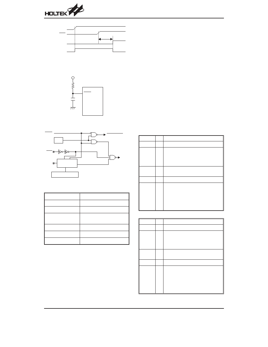
To guarantee that the system oscillator has started and
stabilized, the SST (System Start-up Timer) provides an
extra-delay of 1024 system clock pulses after a system
power up or when awakening from a HALT state.
When a system power up occurs, the SST delay is
added during the reset period. But when the reset co-
mes from the RES pin, the SST delay is disabled. Any
wake-up from HALT will enable the SST delay.
HT86XXX
Rev. 1.70
25
May 6, 2004
Reset Timing Chart
Reset Circuit
Reset Configuration
The function unit chip reset status are shown below.
PC
000H
Interrupt
Disable
Prescaler
Clear
WDT
Clear. After master reset,
WDT begins counting
Timer/event counter
Off
Input/output ports
Input mode
SP
Points to the top of the stack
Timer/Event Counter 0/1
There are four timer counters are implemented in the
HT86XXX. The Timer/Event Counter 0 and 1 contain
16-bit programmable count-up counters whose clock
may come from an external source or the system clock
divided by 4 (T1). Using the internal instruction clock
(T1), there is only one reference time base. The external
clock input allows the user to count external events,
measure time intervals or pulse width, or to generate an
accurate time base.
There are three registers related to Timer/Event Coun-
ter 0; TMR0H (0CH), TMR0L (0DH), TMR0C (0EH).
Writing to TMR0L only writes the data into a low byte
buffer. Writing to TMR0H will write the data and the con-
tents of the low byte buffer into the Timer/Event Counter
0 preload register (16-bit) simultaneously. The
Timer/Event Counter 0 preload register is changed only
by a write to TMR0H operation. Writing to TMR0L will
keep the Timer/Event Counter 0 preload register un-
changed.
Reading TMR0H will also latch the TMR0L into the low
byte buffer to avoid false timing problems. Reading the
TMR0L only returns the value from the low byte buffer
which may be a previously loaded value. In other words,
the low byte of Timer/Event Counter 0 cannot be read di-
rectly. It must read the TMR0H first to ensure that the
low byte contents of Timer/Event Counter 0 are latched
into the buffer.
There are three registers related to the Timer/Event
Counter 1; TMR1H (0FH), TMR1L (10H), TMR1C (11H).
The Timer/Event Counter 1 operates in the same man-
ner as Timer/Event Counter 0.
Label
Bits
Function
¾
0~2 Unused bit, read as
²0²
TE
3
To define the TMR0/TMR1 active
edge of timer/event counter
(0=active on low to high;
1=active on high to low)
TON
4
To enable/disable timer counting
(0=disabled; 1=enabled)
¾
5
Unused bit, read as
²0²
TM0,
TM1
6
7
To define the operating mode
(TMR1, TMR0)
01=Event count mode (external clock)
10=Timer mode (internal clock)
11=Pulse width measurement mode
00=Unused
TMR0C/TMR1C Register
Label
Bits
Function
¾
0~2 Unused bit, read as
²0²
TE
3
To define the TMR0/TMR1 active
edge of timer/event counter
(0=active on low to high;
1=active on high to low)
TON
4
To enable/disable timer counting
(0=disabled; 1=enabled)
¾
5
Unused bit, read as
²0²
TM0,
TM1
6
7
To define the operating mode
(TMR1, TMR0)
01=Unused
10=Timer mode (internal clock)
11=Unused
00=Unused
TMR2C Register
t
S S T
R E S
V D D
S S T T i m e - o u t
C h i p R e s e t
R E S
V
D D
W D T
H A L T
W D T
T i m e - o u t
R e s e t
R E S
C o l d
R e s e t
W a r m R e s e t
P o w e r - o n D e t e c t i n g
S S T
1 0 - s t a g e
R i p p l e C o u n t e r
O S C I
HT86XXX
Rev. 1.70
26
May 6, 2004
The TMR0C is the Timer/Event Counter 0 control regis-
ter, which defines the Timer/Event Counter 0 options.
The Timer/Event Counter 1 has the same options as the
Timer/Event Counter 0 and is defined by TMR1C.
The timer/event counter control registers define the op-
erating mode, counting enable or disable and active
edge.
The TM0, TM1 bits define the operating mode. The
event count mode is used to count external events,
which implies that the clock source comes from an ex-
ternal (TMR0/TMR1 is connected to PC4/PC5) pin. The
timer mode functions as a normal timer with the clock
source coming from the instruction clock. The pulse
width measurement mode can be used to count the high
o r l o w l e v e l d u r a t i o n o f a n e x t e r n a l s i g n a l
(TMR0/TMR1). The counting method is based on the in-
struction clock.
In the event count or timer mode, once the timer/event
counter starts counting, it will count from the current
contents in the timer/event counter to FFFFH. Once an
overflow occurs, the counter is reloaded from the
timer/event counter preload register and generates a
corresponding interrupt request flag (T0F/T1F; bit 5/6 of
INTC) at the same time.
In the pulse width measurement mode with the TON and
TE bits equal to one, once the TMR0/TMR1 has re-
ceived a transient from low to high (or high to low; if the
TE bit is 0) it will start counting until the TMR0/TMR1 re-
turns to the original level and resets TON. The mea-
sured result will remain in the timer/event counter even if
the activated transient occurs again. In other words,
only one cycle measurement can be done. When TON
is set again, the cycle measurement will function again
as long as it receives further transient pulses. Note that,
in this operating mode, the timer/event counter starts
counting not according to the logic level but according to
the transient edges. In the case of counter overflows,
the counter is reloaded from the timer/event counter
preload register and issues the interrupt request just like
in the other two modes.
To enable the counting operation, the Timer ON bit
(TON; bit 4 of TMR0C/TMR1C) should be set to 1. In the
pulse width measurement mode, TON will be cleared
automatically after the measurement cycle is complete.
But in the other two modes TON can only be reset by in-
struction. The overflow of the timer/event counter is one
of the wake-up sources. No matter what the operation
mode is, writing a 0 to ET0I/ET1I can disable the corre-
sponding interrupt service.
In the case of a Timer/Event Counter OFF condition,
writing data to the timer/event counter preload register
will also reload that data to the timer/event counter. But
if the timer/event counter is turned on, data written to the
timer/event counter will only be kept in the timer/event
counter preload register. The timer/event counter will
continue to operate until an overflow occurs.
When the timer/event counter (reading TMR0H/
TMR1H) is read, the clock will be blocked to avoid er-
rors. As this may result in a counting error, this must be
taken into consideration by the programmer.
Timer Counter 2
The timer counter TMR2 is also a 16-bit programmable
count-up counter. It operates in the same manner as
Timer/Event Counter 0/1, but the clock source of TMR2
is from only internal instruction cycle (T1). Therefore
only (TM1,TM0)=(1,0) is allowable.
S y s t e m C l o c k / 4
T M 1
T M 0
T M R 0
T M R 1
T E
T M 1
T M 0
T O N
P u l s e W i d t h
M e a s u r e m e n t
M o d e C o n t r o l
T i m e r / E v e n t C o u n t e r 0 / 1
P r e l o a d R e g i s t e r
T i m e r / E v e n t
C o u n t e r 0 / 1
L o w B y t e
B u f f e r
D a t a B u s
R e l o a d
O v e r f l o w
t o I n t e r r u p t
Timer/Event Counter 0/1
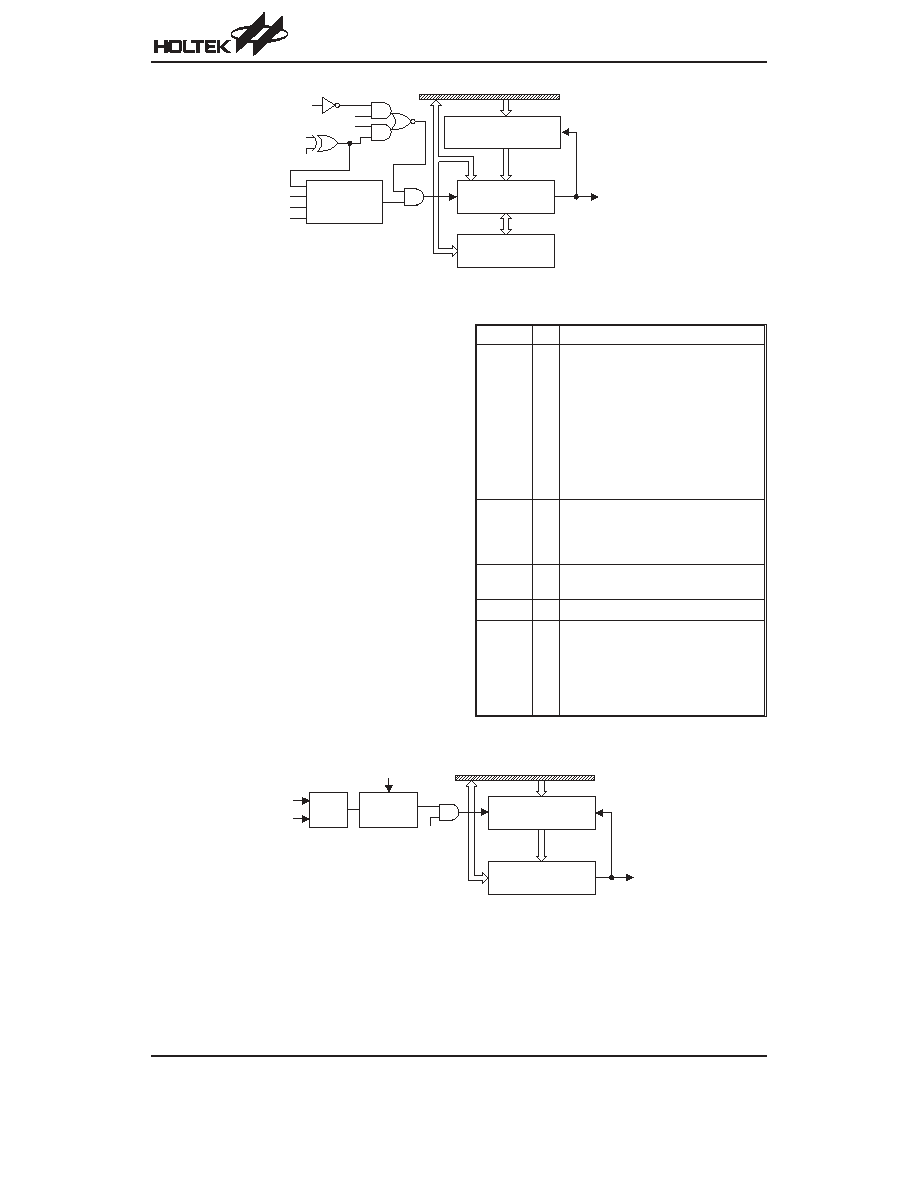
HT86XXX
Rev. 1.70
27
May 6, 2004
Timer Counter 3 (RTC Time Base)
The timer counter TMR3 is an 8-bit programmable
count-up counter. Its counting is as the same manner as
Timer Event Counter 0/1 and Timer Counter 2, but the
clock source of TMR3 can be from internal instruction
cycle (T1) or external 32kHz crystal which is connected
to XIN and XOUT. The TMR3
¢s clock source is deter-
mined by mask option. If the 32kHz crystal is enabled,
then TMR3
¢s clock source is 32kHz which is from XIN
and XOUT. If the 32kHz crystal is disabled, then TMR3
¢s
clock source is internal T1.
The TMR3 is internal clock source only, i.e.
( T M 1 , T M 0 ) = ( 1 , 0 ) . T h e r e i s a 3 - b i t p r e s c a l e r
(TMR3S2,TMR3S1,TMR3S0) which defines different
division ratio of TMR3
¢s clock source.
Label
Bits
Function
TMR3S2,
TMR3S1,
TMR3S0
0~2
To define the operating clock source
(TMR3S2, TMR3S1, TMR3S0)
000: clock source/2
001: clock source/4
010: clock source/8
011: clock source/16
100: clock source/32
101: clock source/64
110: clock source/128
111: clock source/256
TE
3
To define the TMR3 active edge of
timer/event counter
(0=active on low to high;
1=active on high to low)
TON
4
To enable/disable timer counting
(0=disabled; 1=enabled)
¾
5
Unused bit, read as
²0²
TM0,
TM1
6
7
To define the operating mode
(TM1, TM0)
01=Unused
10=Timer mode (internal clock)
11=Unused
00=Unused
TMR3 Register
S y s t e m C l o c k / 4
T M 1
T M 0
T E
T M 1
T M 0
T O N
P u l s e W i d t h
M e a s u r e m e n t
M o d e C o n t r o l
T i m e r / E v e n t C o u n t e r 2
P r e l o a d R e g i s t e r
T i m e r / E v e n t
C o u n t e r 2
L o w B y t e
B u f f e r
D a t a B u s
R e l o a d
O v e r f l o w
t o I n t e r r u p t
G N D
Timer Counter 2
S y s t e m C l o c k / 4
8 - S t a g e
P r e s c a l e r
T i m e r C o u n t e r 3
P r e l o a d R e g i s t e r
D a t a B u s
R e l o a d
O v e r f l o w
t o I n t e r r u p t
T i m e r C o u n t e r 3
T O N
M a s k
O p t i o n
3 2 K C r y s t a l
( T M R 3 S 2 , T M R 3 S 1 , T M R 3 S 0 )
Timer Counter 3

HT86XXX
Rev. 1.70
28
May 6, 2004
The registers states are summarized in the following table.
Register Reset (Power On)
WDT Time-out
(Normal Operation)
RES Reset
(Normal Operation)
RES Reset
(HALT)
WDT Time-out
(HALT)
PC
0000H
0000H
0000H
0000H
0000H
MP0
xxxx xxxx
uuuu uuuu
uuuu uuuu
uuuu uuuu
uuuu uuuu
MP1
xxxx xxxx
uuuu uuuu
uuuu uuuu
uuuu uuuu
uuuu uuuu
ACC
xxxx xxxx
uuuu uuuu
uuuu uuuu
uuuu uuuu
uuuu uuuu
TBLP
xxxx xxxx
uuuu uuuu
uuuu uuuu
uuuu uuuu
uuuu uuuu
TBLH
xxxx xxxx
uuuu uuuu
uuuu uuuu
uuuu uuuu
uuuu uuuu
WDTS
0000 0111
0000 0111
0000 0111
0000 0111
uuuu uuuu
STATUS
--00 xxxx
--1u uuuu
--uu uuuu
--01 uuuu
--11 uuuu
INTC
-000 0000
-000 0000
-000 0000
-000 0000
-uuu uuuu
TMR0H
xxxx xxxx
uuuu uuuu
uuuu uuuu
uuuu uuuu
uuuu uuuu
TMR0L
xxxx xxxx
uuuu uuuu
uuuu uuuu
uuuu uuuu
uuuu uuuu
TMR0C
00-0 1---
00-0 1---
00-0 1---
00-0 1---
uu-u u---
TMR1H
xxxx xxxx
uuuu uuuu
uuuu uuuu
uuuu uuuu
uuuu uuuu
TMR1L
xxxx xxxx
uuuu uuuu
uuuu uuuu
uuuu uuuu
uuuu uuuu
TMR1C
00-0 1---
00-0 1---
00-0 1---
00-0 1---
uu-u u---
PA
1111 1111
1111 1111
1111 1111
1111 1111
uuuu uuuu
PAC
1111 1111
1111 1111
1111 1111
1111 1111
uuuu uuuu
PB
1111 1111
1111 1111
1111 1111
1111 1111
uuuu uuuu
PBC
1111 1111
1111 1111
1111 1111
1111 1111
uuuu uuuu
PC
1111 1111
1111 1111
1111 1111
1111 1111
uuuu uuuu
PCC
1111 1111
1111 1111
1111 1111
1111 1111
uuuu uuuu
TMR2H
xxxx xxxx
uuuu uuuu
uuuu uuuu
uuuu uuuu
uuuu uuuu
TMR2L
xxxx xxxx
uuuu uuuu
uuuu uuuu
uuuu uuuu
uuuu uuuu
TMR2C
00-0 1---
00-0 1---
00-0 1---
00-0 1---
uu-u u---
TMR3L
xxxx xxxx
uuuu uuuu
uuuu uuuu
uuuu uuuu
uuuu uuuu
TMR3C
00-0 1xxx
00-0 1uuu
00-0 1uuu
00-0 1uuu
uu-u uuuu
INTCH
-000 ---0
-000 ---0
-000 ---0
-000 ---0
-uuu ---u
TBHP
---x xxxx
---u uuuu
---u uuuu
---u uuuu
---u uuuu
DAL
xxxx ----
uuuu ----
uuuu ----
uuuu ----
uuuu ----
DAH
xxxx xxxx
uuuu uuuu
uuuu uuuu
uuuu uuuu
uuuu uuuu
VOL
xxx- ----
uuu- ----
uuu- ----
uuu- ----
uuu- ----
VOICEC
0--0 -00-
u--u -uu-
u--u -uu-
u--u -uu-
u--u -uu-
LATCH0H
xxxx xxxx
uuuu uuuu
uuuu uuuu
uuuu uuuu
uuuu uuuu
LATCH0M
xxxx xxxx
uuuu uuuu
uuuu uuuu
uuuu uuuu
uuuu uuuu
LATCH0L
xxxx xxxx
uuuu uuuu
uuuu uuuu
uuuu uuuu
uuuu uuuu
LATCH1H
xxxx xxxx
uuuu uuuu
uuuu uuuu
uuuu uuuu
uuuu uuuu
LATCH1M
xxxx xxxx
uuuu uuuu
uuuu uuuu
uuuu uuuu
uuuu uuuu
LATCH1L
xxxx xxxx
uuuu uuuu
uuuu uuuu
uuuu uuuu
uuuu uuuu
LATCHD
xxxx xxxx
uuuu uuuu
uuuu uuuu
uuuu uuuu
uuuu uuuu
Note:
²u² means ²unchanged²
²x² means ²unknown²
²-² means ²undefined²
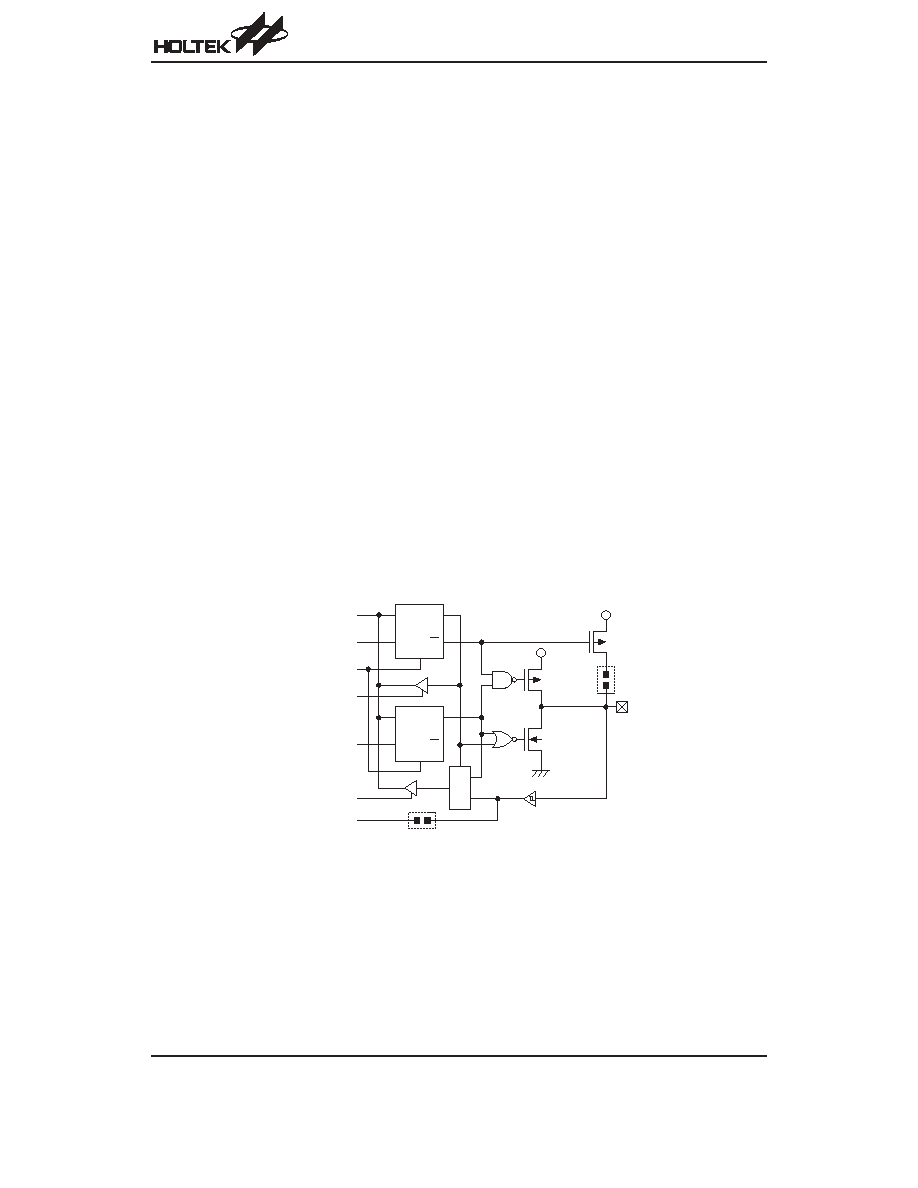
HT86XXX
Rev. 1.70
29
May 6, 2004
Input/Output Ports
There are 23 bidirectional input/output lines in the
microcontroller, labeled from PA to PC, which are
mapped to the data memory of [12H], [14H], and [16H]
respectively. All of these I/O ports can be used for input
and output operations. For input operation, these ports
are non-latching, that is, the inputs must be ready at the
T2 rising edge of instruction
²MOV A, [m]² (m=12H,14H
or 16H). For output operation, all the data is latched and
remains unchanged until the output latch is rewritten.
Each I/O line has its own control register (PAC, PBC,
PCC) to control the input/output configuration. With this
control register, CMOS output or Schmitt trigger input
with or without pull-high resistor structures can be re-
configured dynamically (i.e. on-the-fly) under software
control. To function as an input, the corresponding latch
of the control register must write
²1². The input source
also depends on the control register. If the control regis-
ter bit is
²1², the input will read the pad state. If the con-
trol register bit is
²0², the contents of the latches will
move to the internal bus. The latter is possible in the
²read-modify-write² instruction.
For output function, CMOS is the only configuration.
These control registers are mapped to locations 13H,
15H, and 17H. Bit 7 which is mapped to location [17H] is
always written as
²1².
After a chip reset, these input/output lines remain at high
levels or floating state (dependent on pull-high options).
Each bit of these input/output latches can be set or
cleared by
²SET [m].i² and ²CLR [m].i² (m=12H, 14H,
16H) instructions.
Some instructions first input data and then follow the
output operations. For example,
²SET [m].i², ²CLR
[m].i
², ²CPL [m]², ²CPLA [m]² read the entire port states
into the CPU, execute the defined operations
(bit-operation), and then write the results back to the
latches or the accumulator.
Each line of port A has the capability of waking-up the
device. The wake-up capability of port A is determined
by mask option. There is a pull-high option available for
all I/O lines. Once the pull-high option is selected, all I/O
lines have pull-high resistors. Otherwise, the pull-high
resistors are absent. It should be noted that a
non-pull-high I/O line operating in input mode will cause
a floating state.
By some different mask options, there are 3 shared pins
(PC.4, PC.5, and PC.6) in PC. They can be normal I/O
pins or for special functions. The PC.4 is the external
clock source of timer/event counter TMR0 if TMR0 is set
to external clock mode, and the PC.5 is the external
clock source of timer/event counter TMR1 if TMR1 is set
to external clock mode. PC6 is pin-shared with XIN. The
XIN and XOUT can be connected to a 32kHz crystal as
the clock source of the timer counter TMR3 if the mask
option is set to enable 32kHz (RTC) crystal.
Q
D
C K
S
Q
Q
D
C K
S
Q
M
U
X
D a t a B u s
W r i t e C o n t r o l R e g i s t e r
C h i p R e s e t
R e a d C o n t r o l R e g i s t e r
W r i t e I / O
R e a d I / O
S y s t e m W a k e - U p ( P A o n l y )
W e a k
P u l l - u p
P A 0 ~ P A 7
P B 0 ~ P B 7
P C 0 ~ P C 6
M a s k O p t i o n
M a s k O p t i o n
V
D D
V
D D
Input/Output Ports
HT86XXX
Rev. 1.70
30
May 6, 2004
Audio Output and Volume Control
- DAL, DAH, VOL
The HT86XXX provides one 12-bit current type DAC de-
vice for driving external 8
W speaker through an external
NPN transistor. The programmer must write the voice
data to register DAL (27H) and DAH (28H). The 12-bit
audio output will be written to the higher nibble of DAL
and the whole byte of DAH, and the DAL3~0 is always
read as 0H. There are 8 scales of volume controllable
level that are provided for the current type DAC output.
The programmer can change the volume by only writing
the volume control data to the higher-nibble of the VOL
(29H), and the lower-nibble of VOL (29H) is always read
as 0H.
Voice Control Register
- VOICEC (26H)
The voice control register controls the voice ROM circuit
and DAC circuit, selects voice ROM latch counter, and
controls 32kHz crystal to start in speed-up mode or not.
If the DAC circuit is not enabled, any DAH/DAL output is
invalid. Writing a
²1² to DAC bit is to enable DAC circuit,
and writing a
²0² to DAC bit is to disable DAC circuit. If
the voice ROM circuit is not enabled, then voice ROM
data cannot be accessed at all. Writing a
²1² to VROMC
bit is to enable the voice ROM circuit, and writing a
²0² to
VROMC bit is to disable the voice ROM circuit. The bit 4
(LATCHC) is to determine what voice ROM address
latch counter will be adopted as voice ROM address
latch counter. The bit 7 (FAST) is to determine how to
activate 32kHz crystal of TMR3
¢s clock source.
Label
Bits
Function
¾
0
Unused bit, read as
²0²
DAC
1
Enable/disable DAC circuit
(0= disable DAC circuit;
1= enable DAC circuit)
The DAC circuit is not affected by the
HALT instruction.
T h e s o f t w a r e c o n t r o l s b i t D A C
(VoiceC.1) whether to enable/disable.
VROMC
2
Enable/disable voice ROM circuit
(0= disable voice ROM circuit;
1= enable voice ROM circuit)
¾
3
Unused bit, read as
²0²
LATCHC
4
Select voice ROM counter
(0= voice ROM address latch 0;
1= voice ROM address latch 1)
¾
5, 6 Unused bit, read as
²0²
FAST
7
Enable/disable speed-up 32kHz crys-
tal. Default to 0.
(0= speed-up 32kHz crystal;
1= non-speed-up 32kHz crystal)
Voice ROM Data Address Latch Counter
LATCH0H(18H)/LATCH0M(19H)/LATCH0L(1AH),
LATCH1H(1BH)/LATCH1M(1CH)/LATCH1L(1DH) and
voice ROM data register(2AH)
The voice ROM data address latch counter is the hand-
shaking between the microcontroller and voice ROM,
where the voice codes are stored. One 8-bit of voice
ROM data will be addressed by setting 24-bit address
latch counter LATCH0H/LATCH0M/LATCH0L or
LATCH1H/LATCH1M/LATCH1L. After the 8-bit voice
ROM data is addressed, a few instruction cycles (4
ms at
least) will be cost to latch the voice ROM data, then the
microcontroller can read the voice data from
LATCHD(2AH).
Example: Read an 8-bit voice ROM data which is lo-
cated at address 000007H by address latch 0
set
[26H].2
; Enable voice ROM circuit
clr
[26H].4
; Select voice ROM address
; latch counter 0
mov
A, 07H
;
mov
LATCH0L, A ; Set LATCH0L to 07H
mov
A, 00H
;
mov
LATCH0M, A ; Set LATCH0M to 00H
mov
A, 00H
;
mov
LATCH0H, A ; Set LATCH0H to 00H
call
Delay Time
; Delay a short period of time
mov
A, LATCHD
; Get voice data at 000007H
HT86XXX
Rev. 1.70
31
May 6, 2004
Mask Option
Mask Option
Description
PA Wake-up
Enable/disable PA wake-up function
Watchdog Timer (WDT)
Enable/disable WDT function
One or two CLR instruction
WDT clock source is from WDTOSC or T1
External INT Trigger Edge
External INT is triggered on falling edge only, or is triggered on falling and rising
edge.
Timer 3 Clock Source
Timer3
¢s clock source is from T1, or is from the external 32kHz crystal which is
connected to XIN and XOUT.
External Timer 0/1 Clock Source Enable/disable external timer of timer 0 and timer 1, share with PC4 and PC5.
PA Pull-high
Enable/disable PA pull-high
PB Pull-high
Enable/disable PB pull-high
PC Pull-high
Enable/disable PC pull-high
f
OSC
- R
OSC
Table (V
DD
=3V)
f
OSC
R
OSC
4MHz
±10%
6MHz
±10%
8MHz
±10%
100k
W
75k
W
62k
W
Application Circuits
HT86XXX
Rev. 1.70
32
May 6, 2004
O S C 2
O S C 1
H T 8 6 X X X
V
D D
8 0 5 0
S P K
( 8 W / 1 6 W )
A U D
0 . 1 m F
P A 0 ~ P A 7
P B 0 ~ P B 7
P C 0 ~ P C 6
1 0 0 k W ~ 6 2 k W
R E S
V D D
V
D D
I N T
1 0 0 k W
V
D D
0 . 1 m F
1 0 0 m F
V S S
V S S A
V
D D
V D D A
1 0 W
4 7 m F
0 . 1 m F
N o t e : R 1 > R 2
R 1
R 2
O S C 2
O S C 1
H T 8 6 X X X
A U D
4 M H z ~ 8 M H z
1
2
3
4
5
6
7
8
H T 8 2 V 7 3 3
V
D D
4 7 m F
0 . 1 m F
1 0 m F
O U T N
V D D
V R E F
N C
O
U
T
P
C E
A u d i o I n
A u d i o I n
R E S
V D D
V
D D
I N T
1 0 0 k W
V
D D
0 . 1 m F
1 0 0 m F
V S S
V S S A
V
D D
V D D A
1 0 W
4 7 m F
0 . 1 m F
P A 0 ~ P A 7
P B 0 ~ P B 7
P C 0 ~ P C 6
S P K
( 8 W / 1 6 W )
Package Information
28-pin SOP (300mil) Outline Dimensions
Symbol
Dimensions in mil
Min.
Nom.
Max.
A
394
¾
419
B
290
¾
300
C
14
¾
20
C
¢
697
¾
713
D
92
¾
104
E
¾
50
¾
F
4
¾
¾
G
32
¾
38
H
4
¾
12
a
0
°
¾
10
°
HT86XXX
Rev. 1.70
33
May 6, 2004
2 8
1
1 5
1 4
A
B
C
D
F
C '
G
H
a
E
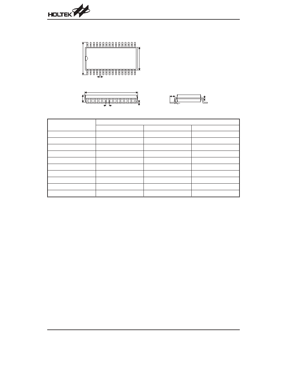
32-pin SOP (450mil) Outline Dimensions
Symbol
Dimensions in mil
Min.
Nom.
Max.
A
543
¾
557
B
440
¾
450
C
14
¾
20
C
¢
¾
¾
817
D
100
¾
112
E
¾
50
¾
F
4
¾
¾
G
32
¾
38
H
4
¾
12
a
0
°
¾
10
°
HT86XXX
Rev. 1.70
34
May 6, 2004
3 2
1
1 7
1 6
A
B
C
D
F
C '
G
H
a
E
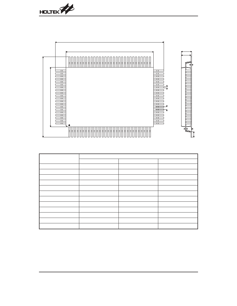
100-pin QFP (14
´20) Outline Dimensions
Symbol
Dimensions in mm
Min.
Nom.
Max.
A
18.50
¾
19.20
B
13.90
¾
14.10
C
24.50
¾
25.20
D
19.90
¾
20.10
E
¾
0.65
¾
F
¾
0.30
¾
G
2.50
¾
3.10
H
¾
¾
3.40
I
¾
0.10
¾
J
1
¾
1.40
K
0.10
¾
0.20
a
0
°
¾
7
°
HT86XXX
Rev. 1.70
35
May 6, 2004
1 0 0
8 1
8 0
5 1
5 0
3 1
3 0
1
A
B
C
D
E
F
G
H
I
J
K
a
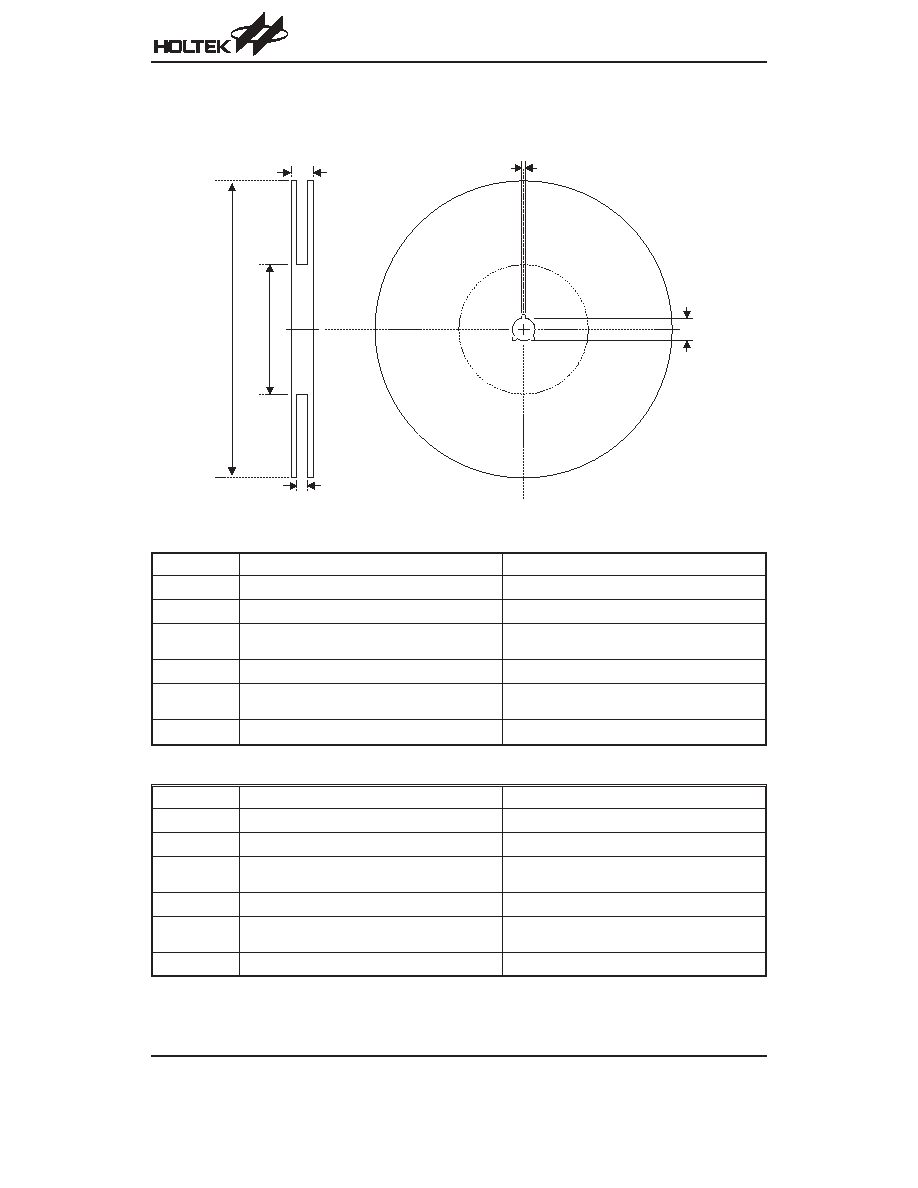
Product Tape and Reel Specifications
Reel Dimensions
SOP 28W (300mil)
Symbol
Description
Dimensions in mm
A
Reel Outer Diameter
330
±1.0
B
Reel Inner Diameter
62
±1.5
C
Spindle Hole Diameter
13.0+0.5
-0.2
D
Key Slit Width
2.0
±0.5
T1
Space Between Flange
24.8+0.3
-0.2
T2
Reel Thickness
30.2
±0.2
SOP 32W
Symbol
Description
Dimensions in mm
A
Reel Outer Diameter
330
±1.0
B
Reel Inner Diameter
100
±0.1
C
Spindle Hole Diameter
13.0+0.5
-0.2
D
Key Slit Width
2.0
±0.5
T1
Space Between Flange
32.8+0.3
-0.2
T2
Reel Thickness
38.2+0.2
HT86XXX
Rev. 1.70
36
May 6, 2004
A
C
B
T 1
T 2
D
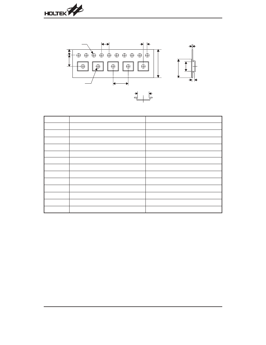
Carrier Tape Dimensions
SOP 28W (300mil)
Symbol
Description
Dimensions in mm
W
Carrier Tape Width
24.0
±0.3
P
Cavity Pitch
12.0
±0.1
E
Perforation Position
1.75
±0.1
F
Cavity to Perforation (Width Direction)
11.5
±0.1
D
Perforation Diameter
1.5+0.1
D1
Cavity Hole Diameter
1.5+0.25
P0
Perforation Pitch
4.0
±0.1
P1
Cavity to Perforation (Length Direction)
2.0
±0.1
A0
Cavity Length
10.85
±0.1
B0
Cavity Width
18.34
±0.1
K0
Cavity Depth
2.97
±0.1
t
Carrier Tape Thickness
0.35
±0.01
C
Cover Tape Width
21.3
HT86XXX
Rev. 1.70
37
May 6, 2004
P
D 1
W
P 1
P 0
D
E
F
t
K 0
B 0
A 0
C
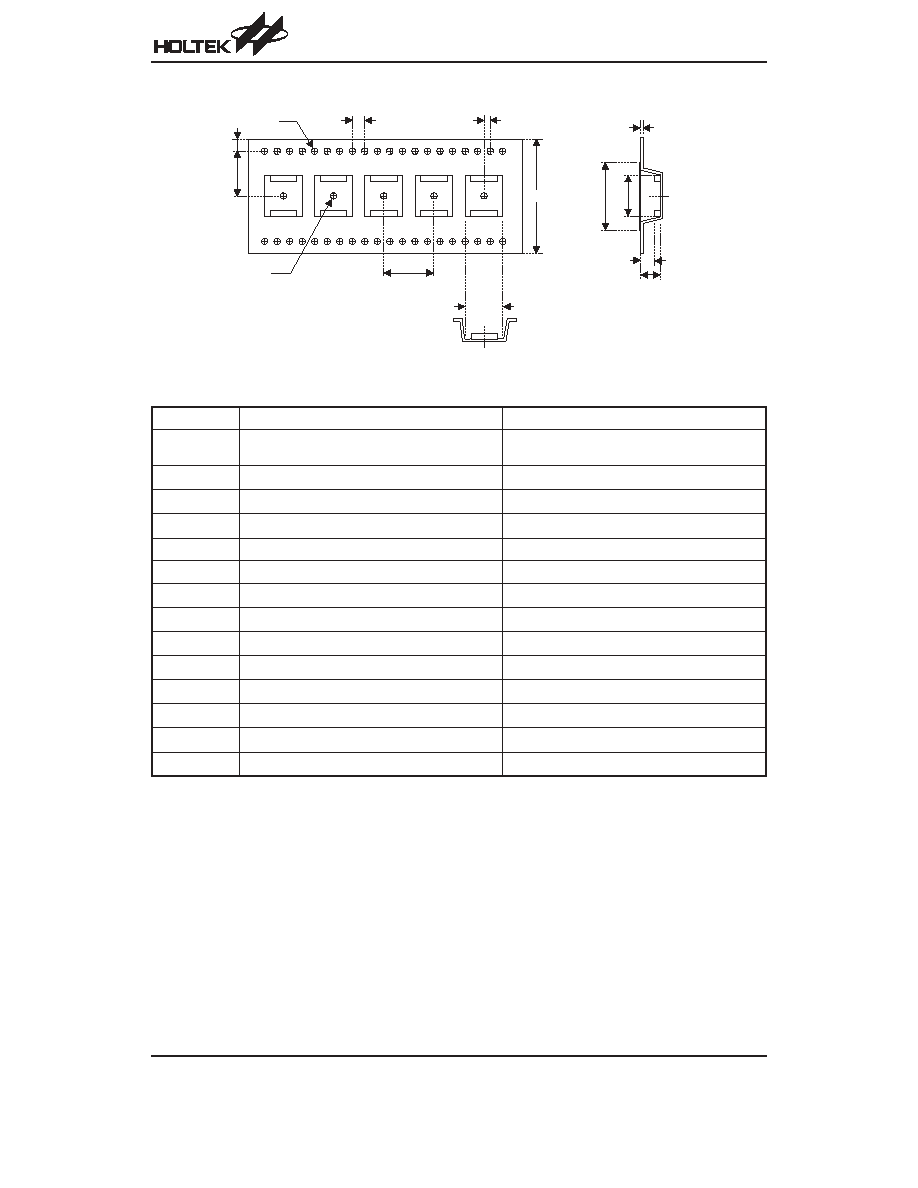
SOP 32W
Symbol
Description
Dimensions in mm
W
Carrier Tape Width
32.0+0.3
-0.1
P
Cavity Pitch
16.0
±0.1
E
Perforation Position
1.75
±0.1
F
Cavity to Perforation (Width Direction)
14.2
±0.1
D
Perforation Diameter
1.55+0.1
D1
Cavity Hole Diameter
2.0+0.25
P0
Perforation Pitch
4.0
±0.1
P1
Cavity to Perforation (Length Direction)
2.0
±0.1
A0
Cavity Length
14.7
±0.1
B0
Cavity Width
20.9
±0.1
K1
Cavity Depth
3.0
±0.1
K2
Cavity Depth
3.4
±0.1
t
Carrier Tape Thickness
0.35
±0.05
C
Cover Tape Width
25.5
HT86XXX
Rev. 1.70
38
May 6, 2004
P
D 1
P 1
P 0
D
E
F
t
K 2
B 0
A 0
W
K 1
C

HT86XXX
Rev. 1.70
43
May 6, 2004
Copyright
Ó 2004 by HOLTEK SEMICONDUCTOR INC.
The information appearing in this Data Sheet is believed to be accurate at the time of publication. However, Holtek as-
sumes no responsibility arising from the use of the specifications described. The applications mentioned herein are used
solely for the purpose of illustration and Holtek makes no warranty or representation that such applications will be suitable
without further modification, nor recommends the use of its products for application that may present a risk to human life
due to malfunction or otherwise. Holtek
¢s products are not authorized for use as critical components in life support devices
or systems. Holtek reserves the right to alter its products without prior notification. For the most up-to-date information,
please visit our web site at http://www.holtek.com.tw.
Holtek Semiconductor Inc. (Headquarters)
No.3, Creation Rd. II, Science Park, Hsinchu, Taiwan
Tel: 886-3-563-1999
Fax: 886-3-563-1189
http://www.holtek.com.tw
Holtek Semiconductor Inc. (Taipei Sales Office)
4F-2, No. 3-2, YuanQu St., Nankang Software Park, Taipei 115, Taiwan
Tel: 886-2-2655-7070
Fax: 886-2-2655-7373
Fax: 886-2-2655-7383 (International sales hotline)
Holtek Semiconductor Inc. (Shanghai Sales Office)
7th Floor, Building 2, No.889, Yi Shan Rd., Shanghai, China 200233
Tel: 021-6485-5560
Fax: 021-6485-0313
http://www.holtek.com.cn
Holtek Semiconductor Inc. (Shenzhen Sales Office)
43F, SEG Plaza, Shen Nan Zhong Road, Shenzhen, China 518031
Tel: 0755-8346
-5589
Fax: 0755-8346
-5590
ISDN: 0755-8346
-5591
Holtek Semiconductor Inc. (Beijing Sales Office)
Suite 1721, Jinyu Tower, A129 West Xuan Wu Men Street, Xicheng District, Beijing, China 100031
Tel: 010-6641
-0030, 6641-7751, 6641-7752
Fax: 010-6641
-0125
Holmate Semiconductor, Inc. (North America Sales Office)
46712 Fremont Blvd., Fremont, CA 94538
Tel: 510-252-9880
Fax: 510-252-9885
http://www.holmate.com
Document Outline
- þÿ
- þÿ
- þÿ
- þÿ
- þÿ
- þÿ
- þÿ
- þÿ
- þÿ
- þÿ
- þÿ
- þÿ
- þÿ
- þÿ
- þÿ
- þÿ
- þÿ